Review

Voltage Lifting Techniques for Non-Isolated DC/DC Converters

School of Electronics, Electrical Engineering and Computer Science (EEECS), Queen’s University, Belfast BT9 5AH, UK
*
Author to whom correspondence should be addressed.
Electronics 2023, 12(3), 718; https://doi.org/10.3390/electronics12030718
Submission received: 28 November 2022 / Revised: 19 January 2023 / Accepted: 24 January 2023 / Published: 1 February 2023
(This article belongs to the Section Power Electronics)

Abstract

:
This paper presents a comprehensive review that highlights the characteristics of non-isolated step-up converters based on high boost voltage lifting techniques. The paper categorises the high boost techniques: multistage/multilevel, switched capacitor, voltage multiplier, voltage lift, switched inductor and magnetic coupling. The paper also discusses in detail the advantages and disadvantages for each category such as cost, complexity, power density, reliability and efficiency. The number of passive and active components, voltage gain, voltage stress, switching frequency, efficiency and power rating are also compared. Although the paper considers coupling inductors in the context of the non-isolated converter, the focus of the entire article is on the non-isolated high voltage step-up techniques. The key contribution in this paper is the review of high boosting techniques rather than the DC /DC converters. This allows divergence of new ideas and new power converters that will help provide highly efficient and flexible power converters for several applications where the sending end voltage is very low as photovoltaic systems. In addition, many applications and control techniques of DC/DC converters are summarised in this paper.

1. Introduction

With the rise of energy consumption over this rapidly industrialising world, there is a pressing need for environmentally non-destructive technological solutions that are economical and efficient at the same time. Forecasting the upcoming challenges like climate change, renewable energy sources (RES) is becoming increasingly important. The expansion of the RES market has brought a lot of interest in technologies like fuel cells and photovoltaics (PVs). PV source is one of the vital energy sources in the world which will be the most favourable energy generation candidate by 2040 since it is clean, reliable and has free emission [1,2]. PV grid connected power systems are evolving in many continents and countries such as Europe, Japan and the US, where such power systems are used in the residential applications [3]. Unfortunately, the output voltage generated from the PV panel is very small compared to the ones already dealt in the traditional power system. This small voltage level also does not meet the requirement for higher voltage electronic equipment, such as X-ray power generators, some servo-motor drives, computer periphery power supplies, the DC backup energy system for an uninterruptible power supply (UPS) and high-intensity-discharge (HID) lamps for automobile headlamps. To obtain higher DC voltage from PV panel, modules can be connected in series [4], but this approach is not preferred for low power applications and it increases reliability and shading problems, which occur by trees, other buildings and clouds [5,6]. For more reliable and efficient operation, PV panels should be connected in parallel as possible to avoid the impact of faulty panels [7]. In some applications such as the microinverter, one panel at low power is enough to be connected to the grid but voltage needs to be highly boosted. In order to optimise the PV output power and utilise the switch voltage blocking capability, the cascaded H-bridge multilevel inverters and other multilevel configurations are applied for grid-connected PV power systems [8,9]. Another method to step up voltage gain utilises voltage divider circuits, but this method suffers from low output voltage and efficiency [10]. Instead of using several PV panels in series connection or voltage divider circuits to increase the voltage conversion ratio, DC/DC converter can be utilised as it is a reliable solution to perform such job especially in low power applications and to provide a controllable voltage [11]. The conventional DC/DC converter needs to be reliable and highly efficient to regulate the DC interface between the source and the DC/AC grid inverter. Typically, 12–48 V from the PV Panel is required to be stepped up to 380 V DC for the full-bridge inverter in the 220 V AC grid-connected power system.
The conventional boost DC/DC converter is used to step up the input voltage to a desired higher level within the practical limit required by the load with very few components. Stepping up the voltage is achieved by storing the energy in the inductor and releasing it to the output at a higher voltage. The boost converter is very popular for capacitive load applications such as photo-flashers and battery chargers. It is also used in automotive applications, power amplifiers, adaptive control applications, battery power systems, consumer electronics, DC motor drives and power factor correction circuits. To obtain a high output voltage, the conventional boost converter must operate at an extremely high duty cycle, but this comes at the expense of the efficiency of the converter and then it is not applicable [12]. The extremely high duty cycle causes high conduction and switching losses; hence, it requires a high current and voltage rated MOSFETs with high ON-state resistance ( R D S ( O N ) ) [13]. It also limits the converter to operate at short off times and low switching frequencies. Short off time is caused by a severe diode reverse-recovery current, thus increasing the electromagnetic interference (EMI) level [14]. Lower switching frequency causes higher ripple current; hence, the output voltage is highly sensitive to changes in the duty cycle and the size of passive elements will be extremely large. With a high duty cycle, there is very little scope for control and, therefore, making a compensating change in the load side is difficult. Furthermore, the conventional boost converter that is implemented performing pulse width modulation using high current and voltage rated MOSFET as the switching device has higher MOSFET ( R D S ( O N ) ) [15]. The main drawbacks of conventional high boost converters are the increased size of passive elements, cost and decreased efficiency.
To overcome the aforementioned drawbacks, there is a need for a topology that could provide conventional boost DC/DC converter with better dynamics, stability, reliability, higher efficiency and higher power density. In addition, the converter should provide low ripple, cost, wide bandwidth, low Electromagnetic Interference (EMI) and fast response to sudden changes [16]. There is an inevitable demand for reliable, efficient, small size and weight step-up DC/DC converter for various power applications. A variety of voltage boosting techniques such as cascaded topologies, interleaved converters, multilevel converters, Switched Capacitor (SC)/Switched Inductor (SL), Voltage Lift (VL) and coupled inductors have been used to efficiently highly boost the voltage in DC/DC converters. The permutation and combination of various voltage boosting techniques, along with various switching topologies and switching cells, create a large range of distinguished topologies.
This paper systematically reviews and categorises high-boosting techniques for DC/DC power converters. The general framework, boosting mechanism, connections, circuit topologies, key features, advantages and disadvantages are established, demonstrated and discussed. Section 2 classifies high step-up techniques. The rest of this paper is organised as follows. Section 3 discusses multistage/multilevel converter including cascaded, symmetric, non-symmetric converters, quadratic boost and interleaved converters. Section 4, Section 5 and Section 6 review switched capacitors, voltage multipliers and voltage lift techniques, respectively. Section 7 discusses switched inductor techniques while Section 8 presents magnetic coupling techniques. Section 9 and Section 10 discuss the applications and control techniques, respectively. Finally, Section 11 draws the conclusion.

2. High Step-Up Techniques

High step-up DC/DC converters, which are used for voltage boosting, are mainly classified as switched capacitors (SCs) (or charge pumps (CPs)), voltage multipliers (VM), switched inductor (SL), voltage lift (VL) and converters with multistage/multilevel structures. Depending on the application, these have merits and demerits in terms of cost, complexity, power density, reliability and efficiency. These classifications are shown in Figure 1. Some of the families classified are distinct to one known technique such as switched capacitor, voltage lift and switched inductor. Other families are extended to a few subfamilies such as the multi-stage family where it has been extended to cascaded, interleaved and multilevel.

3. Multistage/Multilevel Structures

One of the simplest methods of stepping up voltage is connecting various stages of a converter. This can be implemented by integrating symmetric or different converter modules (non-symmetric) with various high voltage gain techniques. The voltage gain increases linearly as a function of the topology used. Broadly, such topologies can be further classified as cascaded, interleaved and multilevel.

3.1. Cascaded Topology

3.1.1. Symmetric and Non-Symmetric Converters

In the general setup of cascaded DC/DC converters Figure 2a,b, two or more symmetric or non-symmetric converters that use two or more controllable switches [17,18,19] or a single switch [20,21,22] can be connected to increase the voltage gain without high duty cycle operation.
As seen in Figure 3a, the low voltage stress on the power switch in the first stage of the cascade enables high frequency operation. A low frequency operates in the second stage [23,24]; hence, the switching losses are reduced [18]. However, a cascaded circuit has two sets of power devices, which makes it not only complex but also expensive [25]. Moreover, both power devices need to be synchronised to prevent the beat frequency from causing circuit stability issues [26]. An n-stage cascade boost converter with a single active switch is presented in [27,28]; such converters are an alternative solution for decreasing the total losses caused by active switches, as shown in Figure 3b. Moreover, they have a simple control circuitry. A comparative study on boost and zeta converters is presented in [29]. A single switch step-up DC/DC converter based on the new SEPIC technology and buck/boost converter [30] is shown in Figure 3c. Its voltage gain is higher than those of SEPIC and buck/boost converters. Therefore, the voltage stress on the power switch is low, and the input current is continuous. An integrated double boost and SEPIC converter (IDBS) is presented in [31] as shown in Figure 3d; it can attain a high voltage conversion ratio at a low duty cycle. The advantages of this combination converter are its capability to achieve a high step-up voltage gain (boost) and a low input current ripple (SEPIC).
Table 1 summarises the following details about symmetric and non-symmetric cascade boost converters: number of components, voltage gain, voltage stress on the main switch, voltage stress of the output diode, input and output voltages, switching frequency and power rating, duty cycle, efficiency, the feature of each DC/DC converter and some popular applications.

3.1.2. Quadratic Boost Converters (QBC)

Figure 4 illustrates the general setup of a quadratic boost converter which comprises one switch, three diodes and four passive elements. A high step-up voltage gain can be obtained by using a quadratic converter Figure 4 at a moderate duty cycle [22,32], but the main drawback of such converters is that the voltage stress on the power switch is equal to the output voltage. Therefore, efficiency is compromised. The conventional quadratic boost converter has a limited voltage gain and is thus unsuitable for high-step-up applications.
Figure 5a shows a quadratic boost converter with a modified VL cell [33]; it achieves a high voltage gain at the output side. Furthermore, it reduces the voltage stress on the power switch, which is an issue with traditional quadratic boost converters. In the literature [34,35,36,37,38,39,40,41,42,43,44,45,46,47,48,49,50,51,52], many DC/DC converters based on quadratic boost converters and modified quadratic boost converters have been proposed to inhibit the dominant constraints in conventional boost converters. A quadratic following boost converter (QFBC) is presented in [38]. It consists of two switches, three capacitors, three diodes and two inductors, and it can step up the voltage gain at a moderate duty cycle. In the modified QFBC (MQFBC) proposed in [39], a bootstrap network is integrated to improve the conventional boost converter. In Figure 5b, a high voltage gain and reduced voltage stress are achieved by using a quadratic boost converter with a coupled inductor [40,41]. However, the power switch suffers from a high voltage stress caused by the leakage inductance of the coupled inductor. Passive clamping circuits are adopted to reduce this high voltage stress. The quadratic boost converter and SEPIC topologies in Figure 5c, which are presented in [42], increase the voltage conversion ratio without an extreme duty ratio. This converter takes advantage of two well-known DC/DC converters, namely, a quadratic boost converter, which has a high step-up capability, and a SEPIC converter which can reduce the input current ripple. A quadratic SEPIC with a switched-coupled inductor, shown in Figure 5d, is proposed in [43] to increase the voltage gain. In [44], a quadratic boost converter and a zeta converter are proposed for a high voltage gain and efficiency. Additionally, both the input and output current ripples are low (features of the quadratic boost converter and zeta converter, respectively). A quadratic boost converter and a Ćuk converter are combined in [45] to provide a high step-up voltage. Two configurations of this proposed converter are shown in Figure 5e,f. The configuration in Figure 5e is called hybrid QBC type I and its voltage stress is lower than the output voltage of the converter. The configuration in Figure 5f is called hybrid QBC type II, and its voltage gain is higher than that of hybrid QBC type I. A novel quadratic boost converter with low inductor currents is proposed in [46]; it can increase the voltage gain as well as the conventional quadratic boost converter can. Furthermore, it has a non-pulsating input current and low voltage stress on the power switch. The main drawback of this converter is its use of two switches. A hybrid cascaded DC/DC converter usually consists of a quadratic boost converter and voltage multiplier circuits. A high voltage gain in [47] is achieved by using a quadratic boost converter and a coupled inductor with an extended voltage doubler cell. Quadratic boost with a voltage multiplier cell was proposed in [48], the output voltage is much higher under the same duty cycle of the traditional quadratic boost converter. Moreover, the input current ripple is low, and the voltage stress is reduced.
Table 2 summarises more details about quadratic boost converter in terms of component number, voltage gain, voltage stress on the main switch, voltage stress of output diode, input and output voltage, switching frequency and power rating, duty cycle, efficiency, feature of each DC/DC converter and applications.

3.2. Interleaved Converters

The interleaved step-up DC/DC converter consists of passive or active clamp circuits and voltage multiplier modules between the input switches and the output diode for providing a high voltage conversion ratio, as shown in Figure 6. However, this technique decreases the current ripple and increases the power density because the input current level in the step-up DC/DC converters is higher than the output current level. Various interleaved DC/DC converters with different techniques can be found in the literature [53,54,55,56,57,58,59,60,61,62].
In Figure 7a, the interleaved converter with voltage multiplier cell proposed in [53] can reduce the input current ripple and improve the power level because the interleaved structure is employed at the input side. Furthermore, the voltage gain is increased at the output side because of the voltage multiplier cell. In Figure 7b, a conventional interleaved boost converter achieves high voltage gain by integrating a voltage multiplier module consisting of switched capacitors and coupled inductors [54,55]. Additionally, it can reduce the input current ripple and doubles the power transfer. In order to increase the voltage gain, the interleaved quadratic boost DC/DC converter has been proposed by using two structures of quadratic boost converter as shown in Figure 7c. It can achieve the voltage gain by using a voltage lift capacitor [56]. In [57], an interleaved step-up converter with a single capacitor snubber is presented. A Winding Crossed Coupled Inductor (WCCI) has been presented in [58] consisting of three winding coupled inductors to boost the voltage gain. In addition, the first phase has two windings, while the second phase has the third winding. To recycle the leakage energy and absorb the voltage spike caused by the leakage inductance, either a passive clamp or an active clamp is adopted [59]. In [60], the proposed converter is an interleaved high step-up DC/DC converter combining with three techniques. However, it takes the advantage of the coupled inductor, switched capacitor and the conventional interleaved boost converter. In order to increase the voltage conversion ratio without using a coupled inductor, a non-isolated high gain interleaved DC/DC converter with reduced voltage stress on semiconductor devices has been proposed in [61]. In Figure 7d, the proposed converter contains two interleaved modified step-up KY converters. The voltage gain is higher than the conventional interleaved boost, Ćuk, ZETA and SEPIC converters. The voltage stress on the semiconductor devices is low; therefore, the efficiency of the proposed converter is increased due to low on-state resistance and low conduction loss. A high step-up interleaved DC/DC converter by combining voltage multiplier and coupled inductor has been proposed in [62]. Two coupled inductors and voltage multiplier are utilised to provide a very high step-up voltage gain; hence, the input current ripple is low because the proposed converter uses the interleaved boost converter at the input side. In addition, it can alleviate the reverse recovery current problem of the diode, and it recycles the leakage energy. Eventually, the efficiency of the proposed converter can be improved by implementing low-voltage-rated MOSFETs with a small on-state resistance which can reduce the conduction loss.
Table 3 summarises more details about the interleaved boost converter in terms of component number, voltage gain, voltage stress on the main switch, voltage stress of output diode, input and output voltage, switching frequency and power rating, duty cycle, efficiency, the feature of each DC/DC converter and some of the common applications.

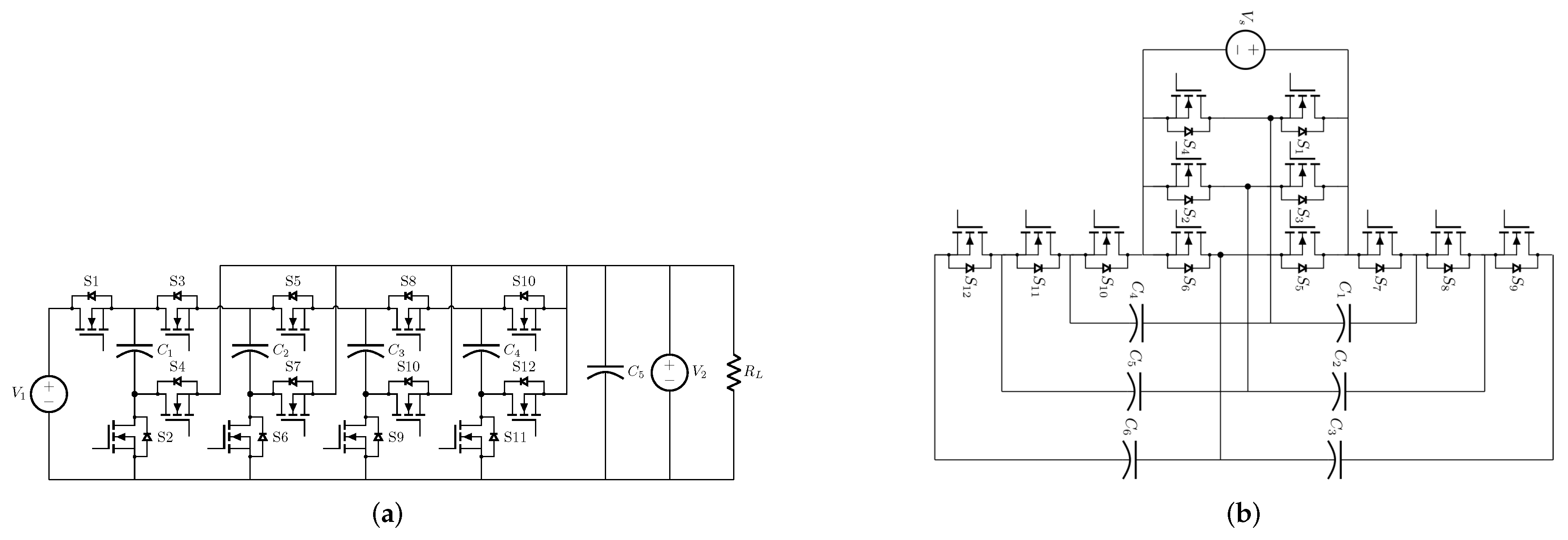
3.3. Multilevel Converters

A Multilevel DC/DC converter helps to decrease or nearly eliminate the magnetic components leading to desirable cost, size, weight, and managing high-temperature operation [63]. Concerning the input voltage, multiple level converters can be categorised into single DC and multiple DC sources groups. Single source multilevel structures are majorly used in electric or fuel cell-based vehicles and traction motors. In contrast, the multiple DC source multilevel converters with cascaded structures are used in modular renewable energy sources such as PV or fuel cells [16].
The switch capacitor structures are usually used in multilevel converter. The Capacitor-Clamped module for multilevel converters in Figure 8a is an essential module for boosting the voltage level, which contains three switches and one capacitor [64,65,66]. In [67], double the DC input voltage can be achieved by utilising two capacitors and four switches, as shown in Figure 8b. PV modules can increase the output voltage level by using a series connection; hence, the DC/DC converter should be used with each PV module to maintain the voltage regulated. The advantages of this connection are higher reliability, higher safety/protection, low maintenance and lower cost [68]. This converter is well known as the Modular Multilevel Converter (MMC) [69,70,71].
Table 4 summarises details about multilevel boost converter in terms of component number, capacitor voltage rating, voltage stress on the main switch, voltage stress of output diode, input and output voltage, switching frequency and power rating, duty cycle, efficiency, the feature of each converter and most common applications of the converter.
Despite its features such as modularity structure, high power density, reliability, the MMC can provide high efficiency and high voltage/current levels. The fundamental multistage/level has shortcomings, such as a complex control scheme and many components. All of this will be relatively heavy, large and bulky. This technique can be used in HVDC transmission, renewable energy systems, DC microgrids, high power DC supply and space technology.

4. Switched Capacitor (SC)

Topologies using SCs are majorly used in low power electronic applications, especially in systems with limited physical dimensions involving higher power density [72]. The concept of SCs is based on charge pump (CP), which is the number of capacitors used in SC cell where the high step-up ratio is attainable [73,74,75,76]. It comprises only capacitors, MOSFETs and diodes, and does not include any inductive element. Their characteristics allow monolithic integration, minimised levels of EMI, and reduced weight and volume [77]. Depending on the non-inverting and inverting cell terms, the polarity of input and output voltages are the same or opposite [78]. As shown in Figure 9, it consists of two capacitors and three diodes, and is placed in conventional DC/DC converters (such as Zeta, SEPIC and Ćuk converters) to build a new converter. The voltage divider circuit describes the functionality of the new converters. During the ON state of the diodes ( D 1 and D 2 ), the capacitors ( C 1 and C 2 ) are charged in parallel. During the OFF state of the diodes ( D 1 and D 2 ), the capacitors ( C 1 and C 2 ) are charged in series. From Figure 9a,e, non-inverting SC or inverting SC are used in many different step-up DC/DC converters. Figure 9a,b are non-inverting and inverting SC cell Zeta converters, respectively. It is developed by utilising the cell of non-inverting and inverting SC instead of the capacitor, the output inductor and the output diode of the conventional Zeta converter. As a result of the additional components, the voltage gain is higher than that achieved by a conventional Zeta converter. Moreover, there is a lower voltage stress on the power switch. Figure 9c depicts a SEPIC converter based on a non-inverting SC cell. Instead of the conventional SEPIC converter’s output diode, the non-inverting SC cell is employed. Compared to a conventional SEPIC converter, it improves the voltage conversion ratio and decreases the voltage stress on the main switch. Figure 9d represents an inverting SC cell Ćuk converter. It is established by modifying the conventional Ćuk converter’s capacitor, output inductor and output diode with an inverted SC cell. However, it boosts the voltage conversion ratio and decreases the switch’s voltage stress. While Figure 9e is a similar circuit to Figure 9d, the voltage doubler cell has been added to the output side. Thus, the voltage gain is higher than the prior circuit and has lower voltage stress. In addition, the Ćuk converter has inductors on both sides, so current flows continuously in both directions. Combining both coupled inductor and switched capacitor [79], an ultra-high step-up DC/DC converter with low voltage stress and high efficiency has been achieved. It does not need extra windings for an ultra-high step-up conversion ratio. In addition, the passive clamp circuit can recycle the leakage energy, which can avoid the voltage spikes across the switch, and the efficiency is increased. The voltage stress on the main switch is lower than the other converter, and it maintains steady for the entire duty cycle range. Moreover, the reverse recovery current problem of the diode is alleviated through the leakage inductance of the coupled inductor.
There are five standard techniques based on SC: Voltage Doubler, Ladder, Dickson, Makowski or Fibonacci, and Series-Parallel. The Voltage Doubler SC is based on two phases, where the switching devices are turning ON and OFF in complement, and the output voltage is double the value of the input voltage [80]. The ladder SC consists of two sets of capacitors. Therefore, the capacitor of the lower ladder is changing the input voltage node, which is made different voltage gain [80]. The Dickson SC can be utilised as a voltage multiplier. In the Dickson SC, the diodes are used to charge pumps instead of active switches. Two strings of pulses with proper phase shift are needed to drive the switching devices, typically at tens of kilohertz or up to megahertz. Another technique based on SC is the Makowski SC; it is also known as Fibonacci because its voltage gain can be boosted according to the Fibonacci number. However, the Makowski SC requires fewer devices to obtain high voltage gain [16]. The voltage regulation ranges of techniques have been limited, and the voltage gains of the circuit are predetermined.
An inductor can be utilised in this topology by replacing one active switch in the five standards SC to achieve higher step-up gain and broad voltage regulations [81]. In order to increase the voltage conversion ratio of step-up DC/DC converter, non-isolated high step-up soft-switching DC/DC converter by using interleaving and Dickson SC techniques have been presented [82]. The advantage of this proposed converter is an improved voltage conversion ratio due to the Dickson SC technique. They can alleviate high current spikes by adding a small resonant inductor into the Dickson SC technique [83,84]. In addition, it can reduce the input current ripple and increase the power density due to interleaving operation.
Table 5 summarises the step-up converter based on the switched-capacitor technique in terms of component number, voltage gain, the voltage stress on the main switch, voltage stress of output diode, input and output voltage, switching frequency and power rating, duty cycle, efficiency, the feature of each DC/DC converter and applications. Despite its features such as cheap, high, lightweight circuits, and small size, SC can provide the converters with a high-power density and fast dynamic response. The fundamentals of SC have shortcomings such as complex modulation and sensitivity to the Equivalent Series Resistance (ESR) of a capacitor. All of this will provide a lack of output voltage regulation. This technique can be used in energy harvesting, mobile displays, automotive applications and high gain DC/DC applications.

5. Voltage Multiplier

Voltage Multiplier circuits contain diodes and capacitors to provide high DC voltage at the output side. Hence, it is efficient, low cost and has a simple structure. The Voltage Multipliers are majorly classified into Voltage Multiplier cells (VMC) and Voltage Multiplier Rectifier (VMR). VMC can be placed after the main switch to reduce its voltage stress, as shown in Figure 10a,b. Moreover, a high voltage conversion ratio and higher efficiency are the other advantages of the VMC. VMR can be placed at the output stage of the transformer or coupled inductor. However, it helps to rectify the AC or pulsating DC voltage. Meanwhile, it acts as a voltage multiplier [16]. The general setup of the volage multiplier rectifier is shown in Figure 10c.
In many applications, the multiplication of the input voltage is applied; hence, various structures have been famous in these cells. In addition, it has low weight, size and cost even if the operation is at high frequency because the bulky capacitors are not used [85]. Some VMCs are also known as switched-diode capacitor voltage multiplier cells, which only contain diodes and capacitors, as shown in Figure 11a,b [86]. For a higher voltage conversion ratio, the inductors of some VMC is required [78]; hence, the power switch can operate with zero current switching (ZCS) [85]. The modified conventional boost converter and modified voltage multiplier cell present a high gain non-isolated DC/DC converter [87]. In [88], a high step-up DC/DC converter based on SEPIC converter is introduced by adopting a coupled inductor with voltage multiplier cell. Low input current ripple, high voltage gain and higher efficiency are the advantages of this converter, which combines two voltage boosting techniques with a SEPIC converter. High step-up DC/DC converter based on a new modified single switch SEPIC (-SEPIC) is proposed in [89]. The output voltage gain can be achieved by adding a coupled inductor and voltage multiplier rectifier (VMR). The advantages of the -SEPIC are continuous input current, zero current switching (ZCS) and low reverse recovery loss. Therefore, the voltage spike on the main switch is low.
There are many different configurations of Half-wave [90] or Full-wave voltage multipliers that contain diodes and capacitors [91]. The Greinacher Voltage Doubler Rectifier (G-VD) is illustrated in Figure 11c, which is used in many DC/DC converters at the output stage of transformer-based converter or multistage converters with modular series output [92]. The shortage of the VMR is the high voltage stress on diodes, and output capacitor voltage is equal to the output voltage. The Cockcroft–Walton (CW) is another voltage multiplier, same as G-VMR, introduced in different year, but it is famous for its cascading structure [93]. A full-bride voltage doubler rectifier is commonly used in various DC/DC converters because its voltage stress on the output capacitor is half the output voltage [94,95]. Sometimes the VMR is considered a voltage triple rectifier; therefore, it can be used in many ultra-step-up DC/DC converters. In isolated structures and multilevel output series structures, the VMR can be applied [96]. Despite its features, such as high voltage ability with simple topology and cell-based structure, voltage multiplier can be integrated into various converters. The voltage multiplier also has shortcomings, such as high voltage stress on components. This needs several cells for high voltage application. This technique can be used in medical (X-ray, laser), high power laser and physics (plasma research, particle accelerator) applications.
Table 6 summarises more details about the step-up converter based on voltage multiplier technique in terms of component number, voltage gain, voltage stress on the main switch, voltage stress of output diode, input and output voltage, switching frequency and power rating, duty cycle, efficiency, the feature of each DC/DC converter and applications.

6. Voltage Lift (VL)

The presence of parasitic elements restricts the output voltage and causes poor transfer efficiency of DC/DC converters. The voltage lift technique provides an excellent opportunity to improve circuit characteristics. The basic structure of the voltage lift is shown in Figure 12. A popular converter that uses VL technique is Luo converter which has been introduced in [97,98]. The capacitor is charged to a specific voltage, and the output voltage is lifted with the voltage level of a charged capacitor.
Depending on the number of capacitors in the circuit, the output voltage can be further re-lifted, triple-lifted and quadruple lifted by reapplying the method as shown in Figure 13a [99,100,101]. The significant advantages of this topology are high power density, high efficiency and cost-effectiveness. In addition, the output voltage ripple is small for high voltage applications. In the literature, various converters, namely, the Ćuk, SEPIC and Zeta converters apply the VL technique [102,103]. The N-Stage quadratic boost converter based on the voltage life technique and voltage multiplier (NQBC-VLVM) described in [37]. By replacing the input inductor of NQBC-VLVM with the VL technique, the voltage conversion ratio with a small duty cycle can be improved. Additionally, the voltage gain can be multiplied by two, which is a benefit of VM, and the voltage stress on the main switch is half the output voltage, leading to higher efficiency. A quadratic boost converter with voltage doubler and voltage life technique is presented in [104,105], which increases the voltage gain four times by utilising the VL technique as shown in Figure 13b. In addition, it can double the voltage gain by using a voltage doubler cell and reduce the voltage stress to half of the output voltage on the main switch. The quadratic boost converter based on the elementary VL technique is proposed in [106] to obtain high voltage gain. Depending on the number of inductors, the proposed converter can exponentially step up the voltage gain. Therefore, the voltage gain of the double lift circuit in Figure 13c is eight times the input voltage, and the voltage gain of the triple lift in Figure 13d is nearly 16 times the input voltage. In contrast, the efficiency decreases with the increase of the number of inductors. In [107], cascaded boost converter based on the double VL technique is proposed. The first stage output of this converter becomes the second stage’s input voltage; hence, it can achieve high voltage gain and low voltage stress on the switches at a low duty cycle.
Table 7 summarises more details about step-up converter based on voltage lift (VL) technique in terms of component number, voltage gain, the voltage stress on the main switch, voltage stress of output diode, input and output voltage, switching frequency and power rating, duty cycle, efficiency, the feature of each DC/DC converter and applications. VL technique has some features such as simple structure, less voltage stress on the switch and high-power density, the fundamentals of VL have some drawbacks such as the need for more passive components. This technique can be used in mid-range DC/DC converters and high gain DC/DC applications.

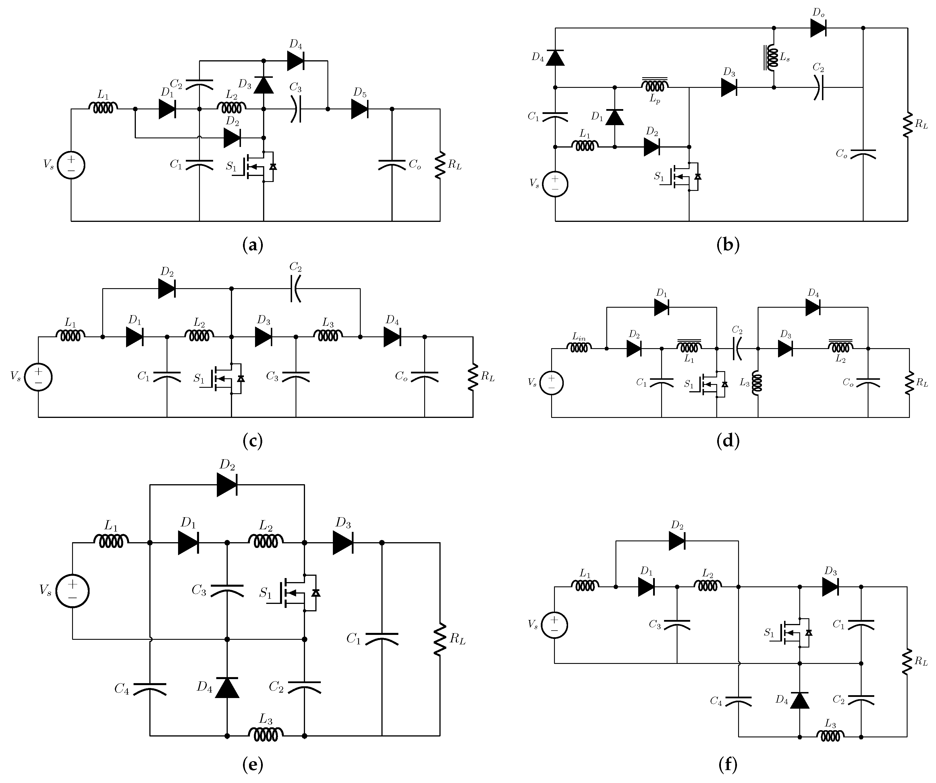
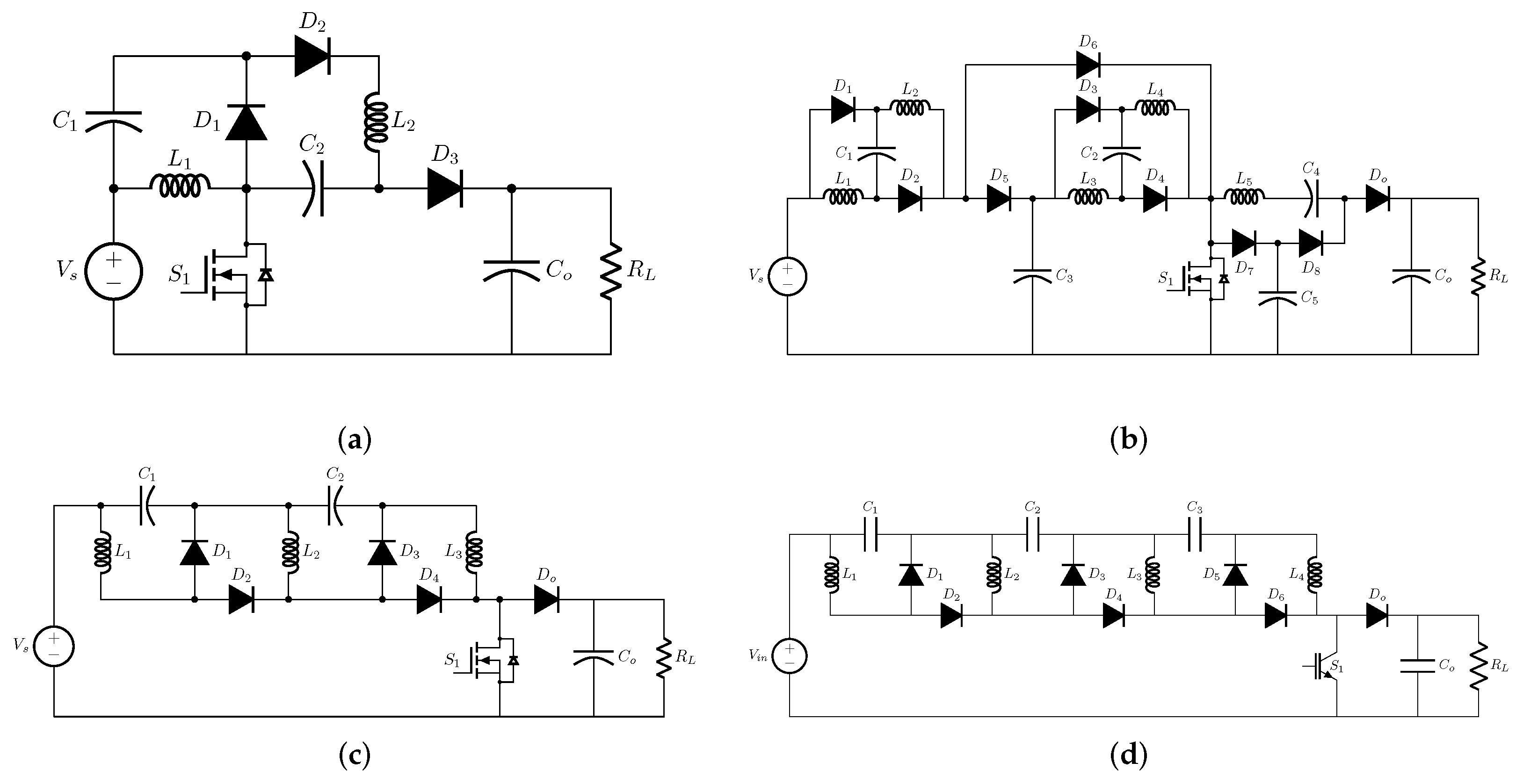
7. Switched Inductor (SL)

The basic Switched Inductor (SL) cell is illustrated in Figure 14. The main operation of such cell is that inductors are charged in parallel and discharged in series. This kind of operation was first introduced in [86]. The input inductor replaces a hybrid boost converter in a conventional boost converter to switched inductor circuit. Hence, it provides a higher voltage gain than the conventional boost converter.
These two inductors can be integrated into a single inductor because they have the same inductance, which helps reduce the size and weight of the converter. Recently, a high voltage conversion ratio DC/DC converter has been achieved by adding a small resonant inductor to the primary VL cell’s circuit and replacing the output diode ( D o ) [108]. A simple structure and high efficiency are the main advantages of this converter. The self-lift SL cell is formed by implementing the elementary VL cell in the SL cell, and the double self-lift SL cell is formed by adding another diode and capacitor to the self-lift SL cell [109]. Therefore, the double self-lift SL cell switch is an operation in reverse using ( S o ) instead of ( D o ) the primary SL cell. For high voltage gain, a transformer-less step-up DC/DC converter based on a switched inductor (SL) and switched capacitor (SC) techniques have been proposed in [110]. Furthermore, it can reduce the voltage stress on the semiconductor switches, but the cost will increase because of the two switches. In Figure 15a, another topology that can provide a high step-up single switch DC/DC converter integrated with a switched inductor (SL) and switched capacitor was presented in [111]. The advantages of this converter are using only a single switch, and the coupled inductor is not required to achieve the voltage gain and low voltage stress on the switch. The XY converter family is introduced in [112] as shown in Figure 15b,c. They use one or more high step-up techniques at the same time, such as a single inductor, switched inductor (SL), voltage lift switched inductor (VL-SL) and modified voltage lift switch inductor (MVL-SL). This family can attain higher output voltage compared to the traditional converter. Meanwhile, it can provide negative output voltage using a single switch. It is suitable for high step-up applications such as photovoltaic multilevel inverter systems and high voltage automotive applications. In Figure 15d, a high voltage gain is achieved using a switched inductor and voltage multiplier [113]. This is achieved by designing N-level DC/DC converter that contains 2N-1 capacitors, 2N+2 diodes, two inductors and only one switch. However, the voltage gain of this converter depends on the number of levels on the output side.
Table 8 summarises more details about the step-up converter based on switched inductor (SL) technique in terms of component number, voltage gain, voltage stress on the main switch, voltage stress of output diode, input and output voltage, switching frequency and power rating, duty cycle, efficiency, the feature of each DC/DC converter and applications. Despite its features (high boost ability and being amenable in many converters), SL needs more passive components. This kind of converter is not preferable for high power applications. The SL technique can be used in mid-range DC/DC converters and high gain DC/DC applications.

8. Magnetic Coupling
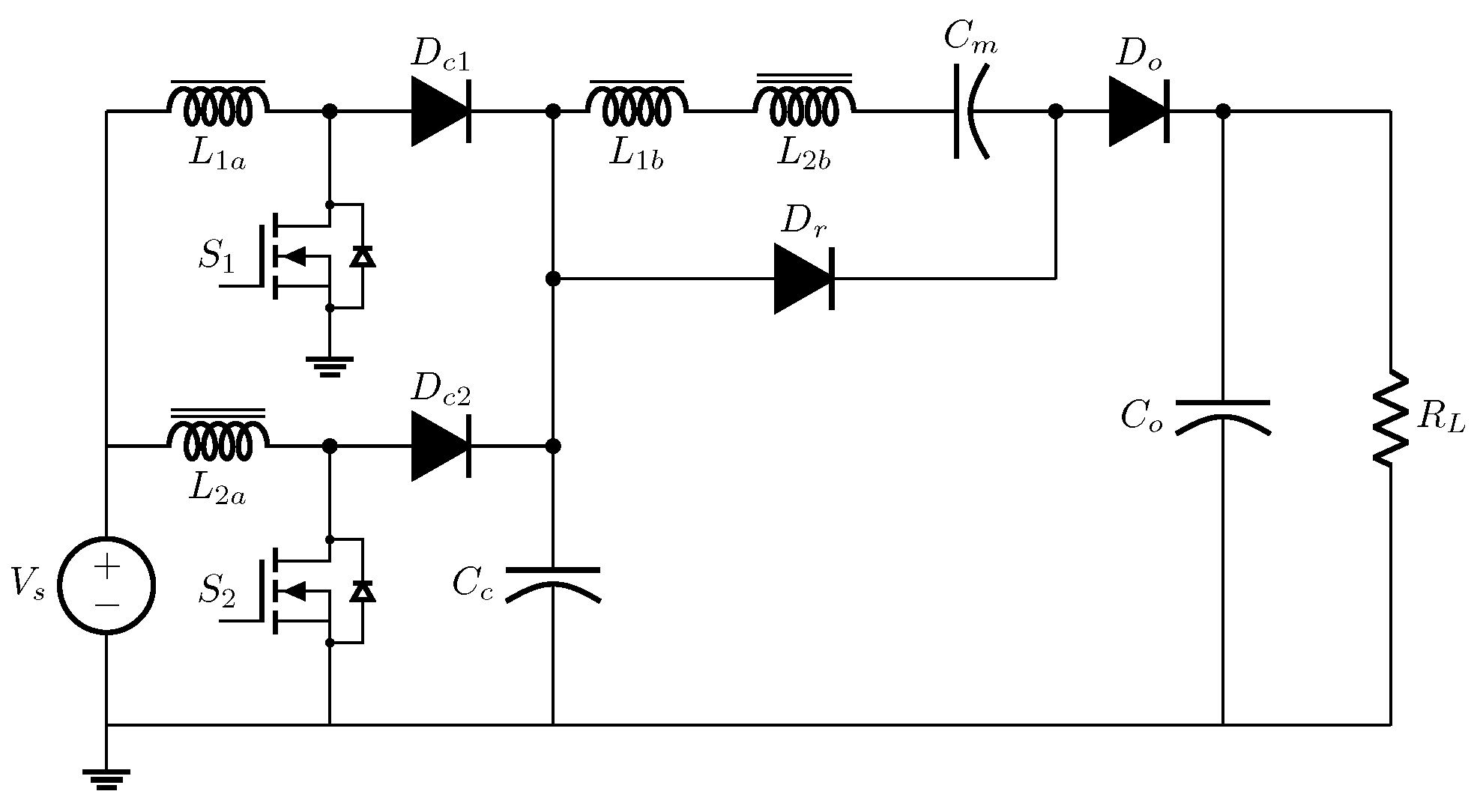
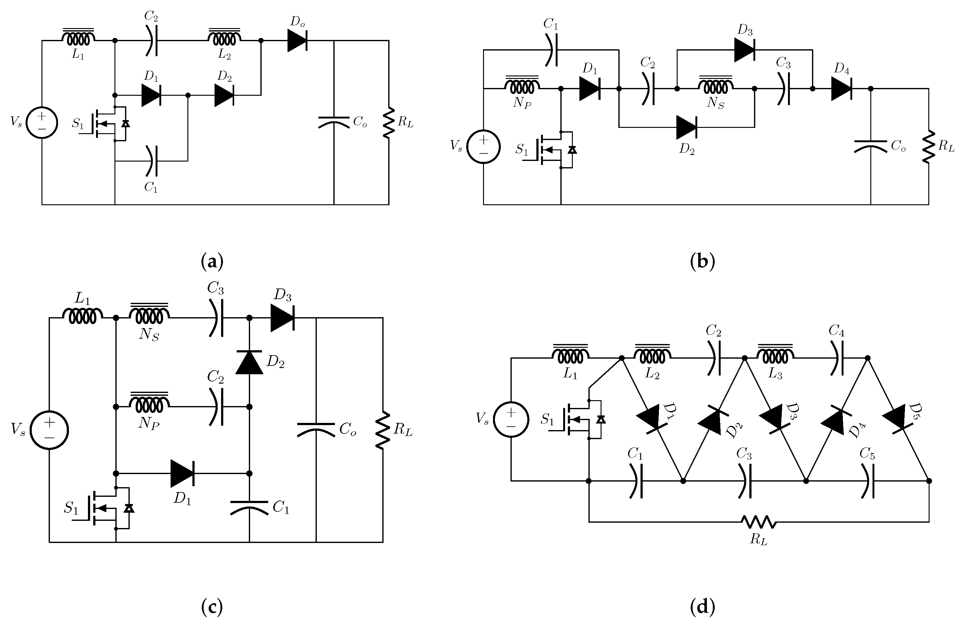
One of the most popular voltage boosting techniques is magnetic coupling, which is used in many DC/DC converters as either non-isolated or isolated converters. The outstanding feature of magnetic coupling is its ability to achieve a higher voltage gain in the output by turning the windings beside the switch duty cycle [114]. The magnetic coupling though has some problems such as leakage inductance [115]. Broadly, it can be further classified as transformer, coupled inductor or multi-track topologies.

8.1. Transformer

An electrical isolated DC/DC converter requires a medium/high frequency transformer, as shown in Figure 16. There are several isolated DC/DC converters that use such device such as full or half-bridge converter, forward converter, push-pull converter and flyback converter. In the past decade, the performance of the conventional DC/DC converter for many applications has been enhanced by using isolated DC/DC converters [116,117,118,119,120,121,122]. Since this literature review intensely focuses on non-isolated DC/DC converters, we will not expand on more detail for isolated topologies.

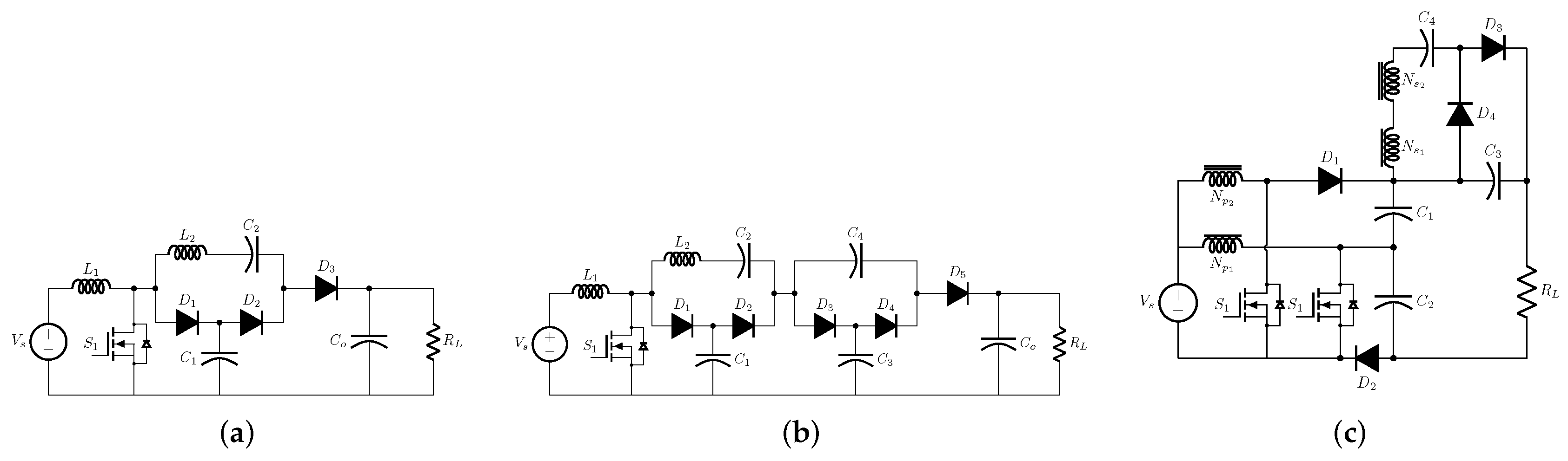
8.2. Coupled Inductor

Since isolation is not required in many applications, coupled inductor circuits can take the advantage of transformer coupling without isolation to increase the voltage in DC/DC converters [123,124,125,126,127,128,129,130,131,132]. Figure 17 shows a general setup for a step-up converter with coupled inductor. The voltage source is a secondary winding, while the clamp capacitor and diode are used to recover the leakage energy recycled directly or through the secondary winding to the load [123]. In addition, a snubber circuit can be used to absorb the energy of the leakage inductance and to improve efficiency [124] as shown in Figure 18a. In [125], a higher voltage gain can be achieved by using a combination of the charge pump and switched capacitor voltage multiplier with a coupled inductor, as shown in Figure 18b, which is helpful in distributed generation systems. A non-isolated high step-up DC/DC converter with continuous input current integrating coupled inductor is introduced in [133] and shown in Figure 18c. It consists of three diodes, three capacitors and one inductor. Further, the coupled inductor in this converter is employed, which achieves higher voltage gain and low input current ripple because the inductor is connected in series to the input. The clamp circuit reduces the voltage stress on the main switch. As a result, low on-state resistance R D S ( O N ) can be achieved, which helps to reduce the conduction losses. Therefore, the switching loss is reduced when the switch is turned on under zero current. A single switch high voltage gain and high-efficiency DC/DC converter are proposed in [134]. The voltage gain is achieved by charging the intermediate capacitors through the coupled inductor in parallel and discharging in series. In [135], a high step-up DC/DC converter based on three winding coupled inductors using two Cockcroft–Walton was proposed, as shown in Figure 18d. Impedance (Z-) source is another area of research in high step-up DC/DC converters. It can increase the voltage gain by using a small duty cycle [136,137,138,139,140].
Table 9 summarises some details on the step-up converter based on the coupled inductor technique in terms of component number, voltage gain, voltage stress on the main switch, voltage stress of output diode, input and output voltage, switching frequency and power rating, duty cycle, efficiency, the feature of each DC/DC converter and applications.

8.3. Multi-Track Structure
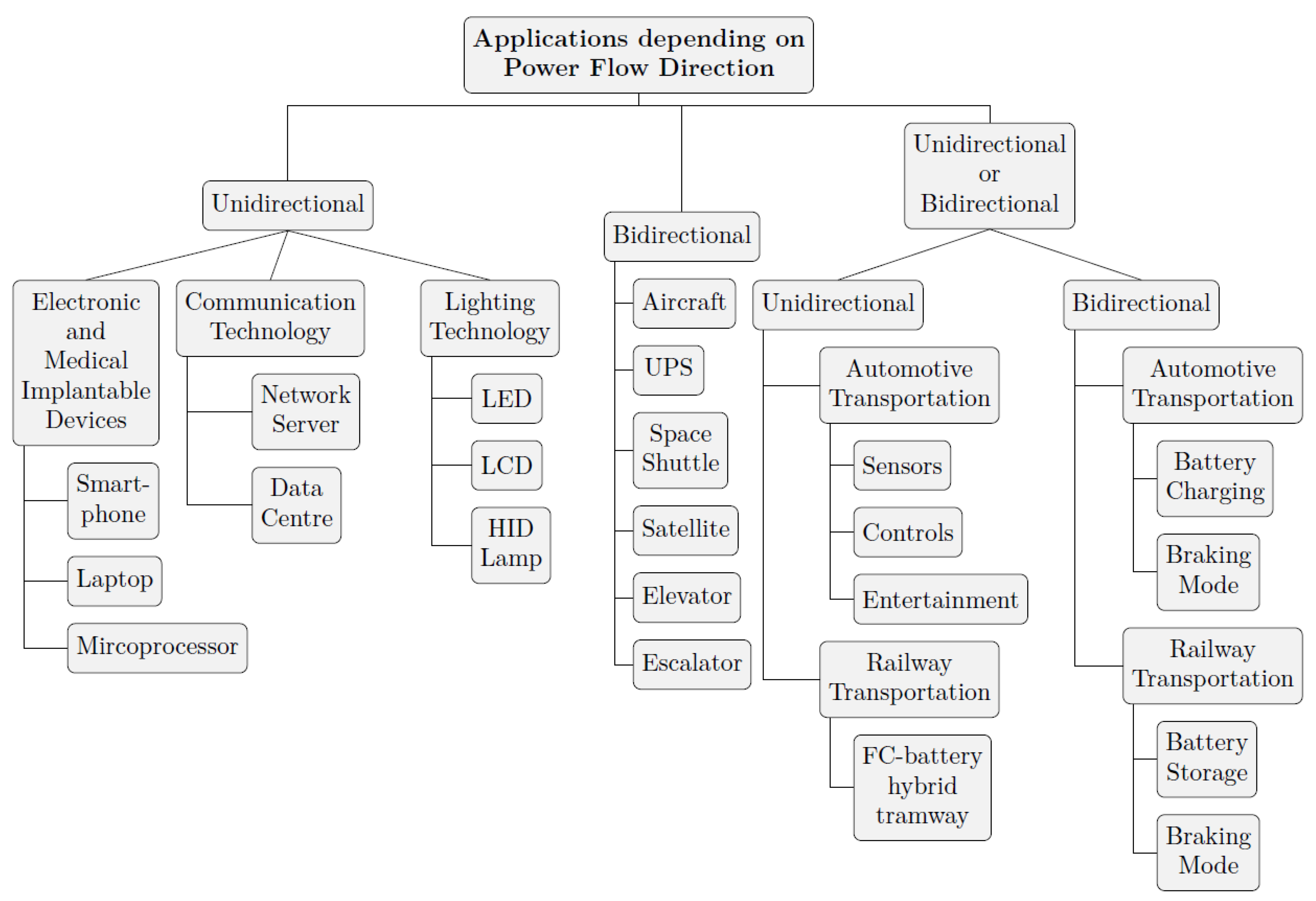
A DC/DC converter can be classified into single-stage structure and multi-stage structure. A single-stage structure can perform multiple functions in a single stage; hence, it is not a complex circuit and has simple control. However, single-stage structure cannot achieve high performance with a wide range of operations. A multi-stage structure can perform one or more function in each stage, which is better in terms of system performance. In contrast, the number of components in this structure is high and the complexity increases.
In the literature [141,142,143,144], the basic block diagram of the multi-stage structures has a switched capacitor, switched inductor and magnetically coupled circuits, which is considered one of the essential solutions. The switched inductor circuits are used for providing voltage regulation, but their size is large and the performance at high voltage conversion ratios, and their power density is limited. The switched capacitor circuits are used for providing balance efficiency, but they cannot have voltage regulation capability. The magnetic circuits provide a high voltage conversion ratio, galvanic isolation and soft switching, but they cannot keep high performance across a wide range of operations. Cascaded two-stage structures for laptop power supply are presented in [145] to provide a high performance. The first stage has a switched capacitor voltage divider, inductor-less, soft switching and high-power density [146]. The second stage is a buck converter in which the power density is lower than the voltage divider, and it can provide regulated bus voltage.
Multi-Track integrates various high voltage techniques with magnetic circuits. In [147], multi-track power conversion is proposed by integrating switched capacitors and magnetics. It merges a hybrid switched capacitor/magnetics circuit structure that splits the wide voltage conversion range into smaller ranges, delivers power in multiple tracks and functionally merges the regulation and isolation stages.
Magnetic coupling has some attractive features such as high design freedom and versatility in boost ability due to tuneable turns ratios of magnetic coupling. Furthermore, providing the converters with a switch can be implemented at the low voltage side to help reduce conduction loss and high efficiency in soft switched operation. However, converters with magnetic coupling have some shortcomings such as adverse effects of leakage inductance, which provides a high voltage spike. In addition, such converters are considered bulky due to the magnetic elements included in their design. This technique can be used in high power/voltage DC supply, high voltage applications, DC microgrids, telecommunication and data centres, regenerative (elevator, tram/trolleybus) and bidirectional (Fuel Cell (FC), PV, UPS, Plug-in Electric Vehicle (P-EV), Hybrid Electric Vehicle (H-EV), Vehicle to Grid (V2G)) applications.

9. Applications

DC/DC converters are essential to the growth of technology in many areas, such as consumer electronics, portable devices [148,149], medical implantable devices [150,151], lighting technology [152,153,154,155], automotive and railway technology [156,157,158], information technology (IT), communications and data centres [159,160], space [161], electrical network, aircraft [162,163], renewable energy [69,164], industrial drives, robotics [165] and high voltage technology (physics research, medical and military) [166,167]. The development of DC/DC converter topologies aims to provide low cost, high efficiency, reliable control switching techniques, elimination of losses and high-power density. Furthermore, boost DC/DC converters are used in ultra-low-power and high-power applications to enhance the voltage of micro energy harvesting sources [168,169] that generate only small amounts of voltage (such as solar [170], microbial FC [171], thermoelectric [172], motion and vibration [173] and piezoelectric energy [174]). In many applications, the step-up DC/DC converters are either unidirectional or bidirectional, depending on the power flow direction, as shown in Figure 19.

9.1. Portable and Medical Implantable Devices

PWM boost DC/DC converters and other topology converters are commonly used in such applications because of their uncomplicated nature, small size and low weight. In [175], a 1.5 V alkaline or NiMH battery has a low voltage incompatible with the microprocessor voltage range of 3.3 to 5 V in portable electronic devices or MOSFET gate drivers. Therefore, a single system-on-a-chip (SOC) is employed to enhance the voltage from low to high. Wireless power transfer (WPT) technology is growing a broad application sector in various low power electronics (such as smartphones and laptops [176,177]) and implantable medical devices [150,151]. To achieve WPT requirements for supplying DC load, high step-up DC/DC converters are implemented.

9.2. Lighting Technology and Automotive

High-efficiency DC/DC converters are in high demand in the lighting industry as power supply and driver circuits, for instance. A new generation in lighting has begun with the invention of light-emitting diodes (LED). In [154,155], LED systems provide better lighting because they have a longer life, smaller size and improved robustness. Additionally, LEDs are appropriate for mobile display applications due to their low cost and low energy consumption [152]. Step-up DC/DC converters are utilised as a power supply driver for plasma display panels or as backlight power modules for liquid crystal displays (LCD) [91,154], making them another lighting-related technology. In [156], the low voltage of car batteries (12 V) is required the step-up DC/DC converters to enhance the voltage level for automotive lighting systems that drive high-intensity discharge (HID) lamps and LED spotlights. In [118,178,179,180] the electrification systems such as EV, FC-EV and P-HEV are other examples of automotive transportation in which the range of the battery storage is 180–360V, and the loads are 400–750V. However, the voltage level of the battery should be boosted to match the load’s voltage level.

9.3. Information Technology (IT), Communications, and Space

Different configurations are being developed as a result of the expanding market for IT and telecommunications hardware [159]. Traditional 48-V DC distribution systems have been gradually replaced by 380-V DC systems during the past decade. Therefore, there is a growing need for high step-up DC/DC converters in network servers and data centre applications [160]. In contrast, space shuttle and satellite applications are required high voltage levels of around kilovolts [161,181]. In order to effectively meet the voltage requirements, several different DC/DC converters are utilised in space applications.

9.4. Renewable Energy Sources (RESs) and Aircraft

PV, FC and wind turbines are renewable energy sources that provide power generation flexibility, reliability and portability. In addition, it is considered a free source and emits no CO2. Variable and low voltage (typically 12 to 48 V) is the output voltage of renewable energy sources, which is unsuitable for utility use. Before inverting to an AC grid-connected power system, the DC link voltage must be raised from 350 to 400 VDC [182,183,184]. The most common voltage needs for aircraft electrification [162,163] are a 28-V DC load bus and a 270-V high-voltage DC bus; hence, to achieve low voltage inputs to a high voltage DC bus, high step-up DC/DC converters are commonly used in aircraft systems.

10. Control Techniques

The term control technique plays a significant role in power system operations’ stable and smooth functionality. Herein, if an appropriate and robust design for the controller does not support it, it could result in disturbances and grid instability. Many control techniques are used in the different topologies of the step-up DC/DC converters, and the purpose of the control is to achieve stability at the output side. On the basis of operating conditions and grid behaviour, there are commonly seven types of controllers, namely, linear, nonlinear, predictive, intelligent, robust, adaptive and hybrid control, as illustrated in Figure 20 [185,186].

10.1. Linear Control

Concerning the stability of Micro-Grids (MG) or industrial applications, several linear controller methods are utilised, including Classic Controller (CC) [187,188,189,190], Proportional Resonant Controller (PR) [191], and Linear Quadratic Gaussian Controller (LQG).

10.1.1. Classic Controller (CC)

The CCs are generally considered a basis for linear control techniques in step-up DC/DC converters. The classic controllers’ advantages, which are widely used in many commercial and industrial applications, are their simple structure, easy implementation and realisation. Hence, these generally included Proportional (P), Proportional-Integral (PI) [187,188,189] and Proportional-Integral-Derivative (PID) [190] types. Table 10 summarises some details on classic control in terms of rise time, steady-state error, overshoot, settling time, structure of controller, accuracy, stability and applications.

10.1.2. Proportional Resonant Controller (PR)

PR controllers have been very popular for the past few years, leading to enhanced usage in grid-connected Photovoltaic (PV) systems. PR controllers are highly similar to PI controllers, although in two different operating frames. In this relation, a PR controller generally enables the function of sinusoidal signal tracking in reference frames. In contrast, a PI controller allows for the DC signals tracking in the reference frame. Besides this, another significant difference between PR and PI controllers comes in the integration part. Since PR controllers only integrate frequencies adjacent or near to the resonant frequency, no stationary magnitude errors and phase shifts occur [191].

10.1.3. Linear Quadratic Gaussian Controller (LQG)

The Kalman filter and LQ regulator generally combine to create the LQG controller. Under LQG controllers, functionality and operations are executed evenly and steadily in time-variant and invariant systems [192]. As a state-space technique for developing optimal dynamic regulators, LQG control has advanced significantly in recent years. Instead of focusing on regulation performance and control effort, it considers process disturbances and measurement noise. According to the separation principle of LQG, it is designed and computed separately.

10.2. Non-Linear Control

In contrast to linear controllers, nonlinear controllers execute astounding operations, performance and high dynamic responses. However, such controllers commonly have complicated realisation and design. Apart from this, nonlinear controllers are bifurcated into Sliding Mode Controllers (SMC) [193,194,195,196,197], Partial or Full Feedback Linearisation Controllers (PFL or FFL) [198,199,200] and Hysteresis controllers (HC) [201,202,203,204].

10.2.1. Sliding Mode Controller (SMC)

SMCs are employed for the voltage regulation of Pulse-Width Modulation (PWM) inverters and the variable variation and load disturbances did not influence the SMC controller. In this respect, SMC can be regarded as an adaptive and robust controller operating for system parameter fluctuations on the basis of operating conditions. Consequently, a steady-state response can be realised in-varying systems through SMC in appropriate circumstances. Considering these factors, there is a growing demand for using SMC controllers in PV systems. However, because the controller struggles to adjust to the nonlinear system’s unpredictable dynamic and fluctuating behaviour, it optimises the settings depending on the output ripple waves in order to prevent this problem. Despite all of these benefits aforementioned, SMCs also have some limitations. Firstly, the effectiveness of SMC varies depending on the sliding surface, and choosing an appropriate sliding surface is an extremely difficult task. Secondly, choosing an appropriate sampling time is crucial because insufficient sampling time leads to elevated distortion and degrades the effectiveness of SMC. Thirdly, the SMC main drawback is the chattering effect identified during the tracking process [193]. As a result, to separate the chattering effects, several other controllers are employed along with SMC direct power control as proposed in [194]. This practice removes the disadvantages associated with SMC and facilitates superior control over the active and reactive current and waveforms without incorporating any supplementary current loop. Nevertheless, an undesirable broadband gap of harmonic is formed in this topology. Furthermore, Adaptive, Fuzzy Logic (FLC) and SMC Controllers are combined; hence, the chattering effect could be significantly reduced [195]. In this relation, the FLC is utilised to evaluate the unforeseeable disturbances that emerge because of atmospheric variations, whereas the SMC is employed to manage the inverter performance. Concerning indemnifying the system uncertainties and improving the performance of the inverter, a Fuzzy-Neural Network (FNN) in addition to Fast Terminal Sliding Mode Control (FTSMC) has been proposed in [196]. In [197] SMC is proposed with integrating PI structure in sliding surface, enabling quick response for the system and reducing the steady-state error.

10.2.2. Partial or Full Feedback Linearisation Controller (PFL or FFL)

Under the PFL method, system non-linearities are removed due to the conversion into a partial or complete linear system from the nonlinear system. In this respect, a partially transformed system with non-linearities is referred to as PFL, although, if the system is completely transformed, it would be regarded as an FFL controller. Apart from this, the non-linearities of a system can also be cancelled by instituting nonlinear terms into the system. As a result, they are not restricted to a particular operating point. The grid-injected current and DC link voltage are regulated by employing an FFL controller, as presented in [198]. Concerning structural complexity, system nonlinear features are altered into linear subsystems, and afterwards, a control law is implemented in these subsystems. However, it complicates the PV system and makes it challenging to manage the shifting properties. In the literature [199,200], they updated the control architecture to address these issues.

10.2.3. Hysteresis Controller (HC)

When the reference and grid current is instantly compared, HC can provide the regulated switching pluses for Voltage Source Inverter (VSI). Simplicity, fast transient response, load parameter independence and resilience to changeable parameters are all readily accomplished [201]. The hysteresis controller can function depending on the relay operation, and the signal is filtered for the system’s optimal operation. The controller further reduces the system’s Total Harmonic Distortion (THD) and has an intrinsic current protection system. Nonetheless, HC-controlled systems hold a fundamental issue associated with keeping the measured current inside its band limitations since doing otherwise results in an unwanted fluctuation in the switching frequency. To solve this issue, the literature has a variety of HCC approaches; for instance, a hysteresis controller for grid-tied inverters, as presented in [202,203], could facilitate a stable switching frequency by eliminating the management of the hysteresis band. Furthermore, to preserve a quick transient response, reduce the steady-state error and obtain high resilience, a hybrid solution combining SMC and variable band HCC is also proposed [204].

10.3. Predictive Control (PC)

A PC forecasts the future behaviour of the parameters that must be regulated. It is renowned for its capacity to manage the system’s non-linearities. In addition, the PC can provide the ability to manage current with low harmonic noise distortion because it has a quick dynamic response. However, implementing a PC is more challenging than classic controllers because it requires extensive calculations, and the specific load must be matched [205]. PC is classified into Deadbeat Controller [206,207,208,209] and Model Predictive Controller (MPC) [210,211,212].

10.3.1. Deadbeat Controller

The deadbeat controller is the earliest kind of PC in the category and is utilised in various contemporary applications. In contrast to other digital controllers, a fine-tuned deadbeat controller offers a quick dynamic response. However, one sample delay allows for regulation of the current that it reaches its reference at the end of the following switching cycle. Thus, it is a valuable controller for the inverter current control. High bandwidth is another benefit of the deadbeat controller, providing the system with immediate and instant tracking of the current at essential points. Similarly, a deadbeat controller provides a critical advantage to the system by compensating for errors in the inverter current. Moreover, its sensitivity towards network parameters is also more than other controllers [206,207,208,209].

10.3.2. Model Predictive Controller (MPC)

MPC controller focuses on current parameter precise tracking and reduction in forecasting error. In this sense, MPC facilitates advantages involving balancing all the nonlinear and general network constraints surrounding multiple inputs/outputs. Moreover, based on the parameter’s pre-defined values, MPC forecasts future network values focusing on the stability of its operation. In [210], MPC and finite control set (FCS) are designed for LCL-filtered grid-tied inverters, allowing high-quality current waveforms. However, it is very complex and economical, following many sensor requirements to compute the current (grid injected and invertor side) and voltage (capacitor and grid). Conversely, the proposed FCS-MPC controllers in [211,212] are implemented to 02-level inverters due to their fast-dynamic response, simple structure and capability to easily manage non-linearities and constraints.

10.4. Intelligent Control

Intelligent controllers refer to biological intelligence processed through the automation of things. Intelligent controllers run without using the mathematical modelling system to face single datasets with peculiar information. Intelligent controllers can be classified into a chain of networks which form a path to the overall control strategy of intelligent controllers. These chains of networks include Neural Network Controllers (NNC) [213,214,215], Repetitive Controllers (RC) [216,217] and Fuzzy Logic Controllers (FLC) [218,219,220,221,222,223].

10.4.1. Neural Network Controllers (NNC)

The NN controller is an interlinked approach to control data systems. It is formed of various artificial neurons that emanate from the biological brain system and functions like a human nervous system. In a control system, NN can be used either online or offline to transfer the data through the processes of the controlling system. However, similar to the human psyche, NN also faces work delays, which supports this control strategy’s smooth working. The input and output layer, weights, activation function and closed-loop method for transmitting the information without executing errors in the desired function are the elements in the architectural chain of the NN controlling system. As an adaptive, intelligent and self-improvised controller, NN offers a flexible control system with few designs and operating conditions. NN also ensures stable behaviour and a fast decision-making process to help attain stabilisation in MG [213]. Due to a simplified modelling system, NN controllers are used in various industrial applications [214]. In this respect, wavelet approaches and probabilistic fuzzy neural networks (PFNN) have been used in the NN controlling system to regulate the grid system by handling its reactive power [215]. More importantly, it aims to perform a low-voltage ride throughout the grid system.

10.4.2. Repetitive Controllers (RC)

RCs are also known as internal model principles that facilitate error elimination or reducing strategies. It represents data in pole pairs standing in selected frequencies to highlight errors. The literature studies have indicated a combination of integral controllers, proportional controllers, and resonant controllers as repetitive controllers by connecting in parallel. Their significant advantage is the stability of MG, which aims at harmonising different elements of a grid system, including voltage and current [216]. The repetitive controller is a good performer under non-linear-periodic load, even though its transient response is not highly attractive. However, repetitive controllers can be improved by integrating them in a cascaded or parallel structure of hysteresis and deadbeat. In [217], PI and RC controllers are combined and used in a grid system to tie the PV modules with the inverters. Similarly, in order to enhance the suitability of repetitive controllers in a grid system, m as a weighting factor is used in the PV. It improves the grid system’s capability, agility to respond and resilience.

10.4.3. Fuzzy Logic Controllers (FLC)

FLCs deal with the linguistic values to eliminate the logic of the crisp value in decision making. The FLCs are commonly used in MG, providing highly robust and simple execution. In addition, it minimises overshooting and improves the tracking performance in a grid system [218,219,220,221,222]. In this context, human knowledge is used in forming limits control to identify control parameters and is implemented in control dynamics in the grid system. Four components of forming limits control include Rule base, Fuzzification, Interference mechanism and De-fuzzification [223].

10.5. Robust Control

Based on the principles of Control theory, robust controllers are associated with system uncertainties. In this respect, robust controllers’ goal is based on achieving robust performance and stability even during the imperfect modelling errors are happened. Consequently, a robust controller ensures the balanced performance in single and multi-variable systems. The robust controller is divided into μ -Synthesis Controller and H-Infinity Controller (H).

10.5.1. μ -Synthesis Controller

This method considers the effects of uncertainties—both structured and unstructured—on system performance. This strategy bases the idea of a controller structure on a singular value, which might be an unstructured or structured valve. A μ -synthesis controller is created for 3-phase grid-tied inverters and discusses its significance in various power-related applications [224]. However, this specific controller is not feasible for grid-connected systems because of the imbalanced load situations and large voltage sags.

10.5.2. H-Infinity Controller ( H )

The ( H ) controller is one of the robust controller types. It is called the optimal algorithm for achieving the system’s stabilisation and good performance. This controller is commonly used in actuators. The controller’s main goal is to eliminate the parameter responsible for the system’s disruption. The controller’s benefits include decreased error, a simpler implementation and robustness in the face of unknown parameters. According to this approach, a control issue can only be solved once it is presented as an optimal problem by the controller designer. In addition, the ( H ) approach also has a high computing cost and may tackle problems involving several variables. In order to manage the voltage of the grid-connected Voltage Source Inverters (VSIs), the researchers in [225] recommended a hybrid strategy using repeated H controllers and controllers.

10.6. Adaptive Control

According to the operational conditions of the system, the adaptive controllers can automatically modify the control actions. The load voltage of a 3- Φ inverter is developed with an adaptive controller and a fourth-order load current observer, which exhibits very decent performance even when under non-linear, imbalanced, and abrupt load variations [226]. The high computational complexity of this controller, though, is one of its key drawbacks. The zero steady-state current error in grid inverters is demonstrated [227] using a combined adaptive and deadbeat controller technique. The adaptive controller manages error correction, and both controllers operate simultaneously to maintain a quick dynamic response. By analysing the load and capacitor currents using a single sensor, an adaptive control system based on a resonating filtration system to handle system leading and to offer compensation for the harmonic distortion was proposed [228]. In [229], a non-linear adaptive controller was presented to regulate a grid-connected inverter’s active and reactive power. The controller functions effectively in a variety of atmospheric situations.

10.7. Hybrid Control

Hybrid control is a combination of different types of control techniques. The aim of hybrid control takes any controller’s features to attain the system’s stabilisation. In addition, it achieves a fast response and minimises steady-state error. Many methods of hybrid control are proposed in [191,195,196] and the literature [230,231,232,233,234].

11. Conclusions

Power electronics high boost DC/DC converters are presented to overcome the significant drawbacks of power conversion systems. Non-isolated high boost converters are preferable due to their reduced cost, high efficiency and uncomplicated nature. However, this claim is not accurate for all types of non-isolated converters. This paper analyses, summarises and classifies the advantages and disadvantages of a wide range of state-of-the-art step-up converters based on voltage boosting techniques. The paper categorises the high boost techniques to multistage/multilevel, switched capacitor, voltage multiplier, voltage lift, switched inductor and magnetic coupling. Each category in this paper is discussed in detail, including the advantages and disadvantages of cost, complexity, power density, reliability and efficiency. Meanwhile, this paper also compares the number of passive and active components, voltage gain, voltage stress, switching frequency, efficiency and power rating in Table 1, Table 2, Table 3, Table 4, Table 5, Table 6, Table 7, Table 8 and Table 9. This paper focuses on high boosting techniques rather than the DC/DC converters, allowing divergence of new ideas and new power converters that will help provide highly efficient and flexible power converters for several applications where the sending end voltage is very low, such as photovoltaic systems.
The significant challenges of any step-up DC/DC converter include achieving high voltage gain and reducing the current ripple due to the extreme duty cycle. Moreover, reducing the voltage stress on the power switch can provide a low cost and conduction losses of the power device because the voltage rated and R D S ( O N ) MOSFET are not required to be high. Hence, the switching losses reduce by using soft switching and reverse recovery losses by alleviating the output diode reverse recovery problem.
To achieve the aforementioned challenges, the topology could be integrated with one or two DC/DC converters such as Boost, Ćuk, SEPIC, Zeta and QBC based on one or more techniques such as SC, SL, VL and Voltage Doubler Cell; hence, it allows to take the features of both DC/DC converter and the boosting technique in a single-stage conversion system. In order to obtain eight times voltage gain without operating at an extremely high duty cycle, the Quadratic Boost Converter (QBC) based on the Voltage Doubler Cell and the Voltage Lift (VL) technique is used. Moreover, the voltage doubler cell can double the voltage gain by two times and the voltage stress on the power switch reduces to half of the output voltage. Thereby, it requires a lower voltage rating and R D S ( O N ) MOSFET switch for conduction losses. Hence, reducing switching allows the use of Schottky rectifiers to alleviate the reverse recovery current problem and, thus, the efficiency can be improved.
Another topology increases the conversion ratio without operation at an extremely high duty cycle and high turns ratio; it utilises a coupled inductor and two capacitors with a high step-up DC/DC converter. In addition, the passive clamp circuit recycles the leakage inductance energy of the coupled inductor that can reduce the voltage stress on the power switch. Therefore, it reduces the conduction losses, enabling low resistance R D S ( O N ) .
Eventually, a high step-up conversion ratio, low cost, high efficiency and high-power density are significant DC/DC converter characteristics. However, this paper introduces a clear vision of the general law and framework for the next generation of non-isolated high step-up DC/DC converters.

Author Contributions

Conceptualization, A.A. and A.E.; methodology, A.A.; validation, A.A., A.E. and D.L.; formal analysis, A.E.; investigation, A.A. and A.E.; resources, A.E.; writing—original draft preparation, A.E.; writing—review and editing, A.E.; supervision, A.E. and D.L.; project administration, A.E.; funding acquisition, A.E. All authors have read and agreed to the published version of the manuscript.

Funding

This research was supported in part by the UK Engineering and Physical Sciences Research Council (EPSRC) under Grant EP/T026162/1. For the purpose of open access, the author has applied a Creative Commons Attribution (CC BY) license to any Author Accepted, Manuscript version arising.

Acknowledgments

A. Alkhaldi would like to acknowledge the PhD scholarship provided by Juof University in the Kingdom of Saudi Arabia (KSA) to carry out this research.

Conflicts of Interest

The authors declare no conflict of interest.

References

  1. Figueres, E.; Garcera, G.; Sandia, J.; Gonzalez-Espin, F.; Calvo Rubio, J. Sensitivity Study of the Dynamics of Three-Phase Photovoltaic Inverters With an LCL Grid Filter. IEEE Trans. Ind. Electron. 2009, 56, 706–717. [Google Scholar] [CrossRef]
  2. Li, Q.; Wolfs, P. A Review of the Single Phase Photovoltaic Module Integrated Converter Topologies with Three Different DC Link Configurations. IEEE Trans. Power Electron. 2008, 23, 1320–1333. [Google Scholar] [CrossRef]
  3. Selvaraj, J.; Rahim, N.A. Multilevel Inverter For Grid-Connected PV System Employing Digital PI Controller. IEEE Trans. Ind. Electron. 2009, 56, 149–158. [Google Scholar] [CrossRef]
  4. Shimizu, T.; Wada, K.; Nakamura, N. Flyback-Type Single-Phase Utility Interactive Inverter With Power Pulsation Decoupling on the DC Input for an AC Photovoltaic Module System. IEEE Trans. Power Electron. 2006, 21, 1264–1272. [Google Scholar] [CrossRef]
  5. Li, W.; He, X. Review of Nonisolated High-Step-Up DC/DC Converters in Photovoltaic Grid-Connected Applications. IEEE Trans. Ind. Electron. 2011, 58, 1239–1250. [Google Scholar] [CrossRef]
  6. Scarpa, V.V.R.; Buso, S.; Spiazzi, G. Low-Complexity MPPT Technique Exploiting the PV Module MPP Locus Characterization. IEEE Trans. Ind. Electron. 2009, 56, 1531–1538. [Google Scholar] [CrossRef]
  7. Shimizu, T.; Hashimoto, O.; Kimura, G. A novel high-performance utility-interactive photovoltaic inverter system. IEEE Trans. Power Electron. 2003, 18, 704–711. [Google Scholar] [CrossRef]
  8. Alonso, O.; Sanchis, P.; Gubia, E.; Marroyo, L. Cascaded H-bridge multilevel converter for grid connected photovoltaic generators with independent maximum power point tracking of each solar array. In Proceedings of the IEEE 34th Annual Conference on Power Electronics Specialist, 2003. PESC ’03., Acapulco, Mexico, 15–19 June 2003; Volume 2, pp. 731–735. [Google Scholar] [CrossRef]
  9. Calais, M.; Agelidis, V. Multilevel converters for single-phase grid connected photovoltaic systems-an overview. In Proceedings of the IEEE International Symposium on Industrial Electronics. Proceedings. ISIE’98 (Cat. No.98TH8357), Pretoria, South Africa, 7–10 July 1998; Volume 1, pp. 224–229. [Google Scholar] [CrossRef]
  10. Sivakumar, S.; Sathik, M.J.; Manoj, P.; Sundararajan, G. An assessment on performance of DC–DC converters for renewable energy applications. Renew. Sustain. Energy Rev. 2016, 58, 1475–1485. [Google Scholar] [CrossRef]
  11. Saadat, P.; Abbaszadeh, K. A Single-Switch High Step-Up DC–DC Converter Based on Quadratic Boost. IEEE Trans. Ind. Electron. 2016, 63, 7733–7742. [Google Scholar] [CrossRef]
  12. Forouzesh, M.; Shen, Y.; Yari, K.; Siwakoti, Y.P.; Blaabjerg, F. High-Efficiency High Step-Up DC–DC Converter with Dual Coupled Inductors for Grid-Connected Photovoltaic Systems. IEEE Trans. Power Electron. 2018, 33, 5967–5982. [Google Scholar] [CrossRef]
  13. Robert, W.E.; Dragan, M. Fundamentals of Power Electronics; Springer: Berlin/Heidelberg, Germany, 2001. [Google Scholar]
  14. Fardoun, A.A.; Ismail, E.H. Ultra Step-Up DC–DC Converter With Reduced Switch Stress. IEEE Trans. Ind. Appl. 2010, 46, 2025–2034. [Google Scholar] [CrossRef]
  15. Huber, L.; Jovanovic, M. A design approach for server power supplies for networking applications. In Proceedings of the APEC 2000. Fifteenth Annual IEEE Applied Power Electronics Conference and Exposition (Cat. No.00CH37058), New Orleans, LA, USA, 6–10 February 2000; Volume 2, pp. 1163–1169. [Google Scholar] [CrossRef]
  16. Forouzesh, M.; Siwakoti, Y.P.; Gorji, S.A.; Blaabjerg, F.; Lehman, B. A survey on voltage boosting techniques for step-up DC-DC converters. In Proceedings of the 2016 IEEE Energy Conversion Congress and Exposition (ECCE), Milwaukee, WI, USA, 18–22 September 2016; pp. 1–8. [Google Scholar] [CrossRef]
  17. Morales-Saldana, J.; Gutierrez, E.; Leyva-Ramos, J. Modeling of switch-mode dc-dc cascade converters. IEEE Trans. Aerosp. Electron. Syst. 2002, 38, 295–299. [Google Scholar] [CrossRef]
  18. Wu, T.F.; Yu, T.H. Unified approach to developing single-stage power converters. IEEE Trans. Aerosp. Electron. Syst. 1998, 34, 211–223. [Google Scholar] [CrossRef]
  19. Haroun, R.; Cid-Pastor, A.; Aroudi, A.E.; Martínez-Salamero, L. Synthesis of Canonical Elements for Power Processing in DC Distribution Systems Using Cascaded Converters and Sliding-Mode Control. IEEE Trans. Power Electron. 2014, 29, 1366–1381. [Google Scholar] [CrossRef]
  20. Leyva-Ramos, J.; Ortiz-Lopez, M.; Diaz-Saldierna, L.; Morales-Saldana, J. Switching regulator using a quadratic boost converter for wide DC conversion ratios. IET Power Electron. 2009, 2, 605–613. [Google Scholar] [CrossRef]
  21. López-Santos, O.; Martínez-Salamero, L.; García, G.; Valderrama-Blavi, H.; Mercuri, D.O. Efficiency analysis of a sliding-mode controlled quadratic boost converter. IET Power Electron. 2013, 6, 364–373. [Google Scholar] [CrossRef]
  22. Choudhury, T.R.; Nayak, B. Comparison and analysis of cascaded and Quadratic Boost Converter. In Proceedings of the 2015 IEEE Power, Communication and Information Technology Conference (PCITC), Bhubaneswar, India, 15–17 October 2015; pp. 78–83. [Google Scholar] [CrossRef]
  23. Boujelben, N.; Masmoudi, F.; Djemel, M.; Derbel, N. Design and comparison of quadratic boost and double cascade boost converters with boost converter. In Proceedings of the 2017 14th International Multi-Conference on Systems, Signals and Devices (SSD), Marrakech, Morocco, 28–31 March 2017; pp. 245–252. [Google Scholar] [CrossRef]
  24. Chen, Z.; Yong, W.; Gao, W. PI and Sliding Mode Control of a Multi-Input-Multi-Output Boost-Boost Converter. WSEAS Trans. Power Syst. 2014, 9, 87–102. [Google Scholar]
  25. Amir, A.; Amir, A.; Che, H.S.; Elkhateb, A.; Abd Rahim, N. Comparative analysis of high voltage gain DC-DC converter topologies for photovoltaic systems. Renew. Energy 2019, 136, 1147–1163. [Google Scholar] [CrossRef]
  26. Feng, X.; Liu, J.; Lee, F. Impedance specifications for stable DC distributed power systems. IEEE Trans. Power Electron. 2002, 17, 157–162. [Google Scholar] [CrossRef]
  27. Leyva Ramos, J.; Ortiz-Lopez, M.G.; Morales-Saldana, J.A. Control of a cascade boost converter with a single active switch. In Proceedings of the 2008 IEEE Power Electronics Specialists Conference, Rhodes, Greece, 15–19 June 2008; pp. 2383–2388. [Google Scholar] [CrossRef]
  28. Ortiz-Lopez, M.G.; Leyva-Ramos, J.; Diaz-Saldierna, L.H.; Carbajal-Gutierrez, E.E. Multiloop Controller for N-Stage Cascade Boost Converter. In Proceedings of the 2007 IEEE International Conference on Control Applications, Singapore, 1–3 October 2007; pp. 587–592. [Google Scholar] [CrossRef]
  29. Andrade, A.M.S.S.; Hey, H.L.; Schuch, L.; da Silva Martins, M.L. Comparative Evaluation of Single Switch High-Voltage Step-Up Topologies Based on Boost and Zeta PWM Cells. IEEE Trans. Ind. Electron. 2018, 65, 2322–2334. [Google Scholar] [CrossRef]
  30. Banaei, M.R.; Sani, S.G. Analysis and Implementation of a New SEPIC-Based Single-Switch Buck–Boost DC–DC Converter With Continuous Input Current. IEEE Trans. Power Electron. 2018, 33, 10317–10325. [Google Scholar] [CrossRef]
  31. Sabzali, A.J.; Ismail, E.H.; Behbehani, H.M. High voltage step-up integrated double Boost–Sepic DC–DC converter for fuel-cell and photovoltaic applications. Renew. Energy 2015, 82, 44–53. [Google Scholar] [CrossRef]
  32. Wijeratne, D.S.; Moschopoulos, G. Quadratic Power Conversion for Power Electronics: Principles and Circuits. IEEE Trans. Circuits Syst. Regul. Pap. 2012, 59, 426–438. [Google Scholar] [CrossRef]
  33. Zhang, S.; Xu, J.; Yang, P. A single-switch high gain quadratic boost converter based on voltage-lift-technique. In Proceedings of the 2012 10th International Power and Energy Conference (IPEC), Ho Chi Minh City, Vietnam, 12–14 December 2012; pp. 71–75. [Google Scholar] [CrossRef]
  34. Morales-Saldana, J.A.; Loera-Palomo, R.; Palacios-Hernández, E.; Gonzalez-Martinez, J.L. Modelling and control of a DC-DC quadratic boost converter with R 2 P 2. IET Power Electron. 2014, 7, 11–22. [Google Scholar] [CrossRef]
  35. Ye, Y.m.; Cheng, K.W.E. Quadratic boost converter with low buffer capacitor stress. IET Power Electron. 2014, 7, 1162–1170. [Google Scholar] [CrossRef]
  36. Kadri, R.; Gaubert, J.P.; Champenois, G.; Mostefaï, M. Performance analysis of transformless single switch quadratic boost converter for grid connected photovoltaic systems. In Proceedings of the The XIX International Conference on Electrical Machines - ICEM 2010, Rome, Italy, 6–8 September 2010; pp. 1–7. [Google Scholar] [CrossRef]
  37. Alkhaldi, A.; Akbar, F.; Elkhateb, A.; Laverty, D. N-Stage Quadratic Boost Converter Based on Voltage Lift Technique and Voltage Multiplier. In Proceedings of the The 11th International Conference on Power Electronics, Machines and Drives (PEMD 2022), Newcastle, UK, 21–23 June 2022. [Google Scholar]
  38. Veerachary, M.; Kumar, N. Analysis and Design of Quadratic Following Boost Converter. IEEE Trans. Ind. Appl. 2020, 56, 6657–6673. [Google Scholar] [CrossRef]
  39. Veerachary, M.; Kumar, N. Modified Quadratic Following Boost Converter - Robustness Considerations. In Proceedings of the 2020 IEEE International Conference on Computing, Power and Communication Technologies (GUCON), Greater Noida, India, 2–4 October 2020; pp. 745–750. [Google Scholar] [CrossRef]
  40. Lee, S.W.; Do, H.L. Quadratic Boost DC–DC Converter With High Voltage Gain and Reduced Voltage Stresses. IEEE Trans. Power Electron. 2019, 34, 2397–2404. [Google Scholar] [CrossRef]
  41. Jahangiri, H.; Mohammadpour, S.; Ajami, A. A high step-up DC-DC boost converter with coupled inductor based on quadratic converters. In Proceedings of the 2018 9th Annual Power Electronics, Drives Systems and Technologies Conference (PEDSTC), Tehran, Iran, 13–15 February 2018; pp. 20–25. [Google Scholar] [CrossRef]
  42. Maheshwari, M.; Arounassalame, M. A Novel Integrated High Gain DC-DC Converter. In Proceedings of the 2019 IEEE International Conference on Electrical, Computer and Communication Technologies (ICECCT), Coimbatore, India, 20–22 February 2019; pp. 1–6. [Google Scholar] [CrossRef]
  43. Axelrod, B.; Berkovich, Y.; Beck, Y. New Quadratic Sepic Converter with a Switched-Coupled Inductor. In Proceedings of the 2018 20th European Conference on Power Electronics and Applications (EPE’18 ECCE Europe), Riga, Latvia, 17–21 September 2018; pp. P.1–P.9. [Google Scholar]
  44. Andrade, A.M.S.S.; Martins, M.L.d.S. Quadratic-Boost With Stacked Zeta Converter for High Voltage Gain Applications. IEEE J. Emerg. Sel. Top. Power Electron. 2017, 5, 1787–1796. [Google Scholar] [CrossRef]
  45. Pires, V.F.; Cordeiro, A.; Foito, D.; Silva, J.F. High Step-Up DC–DC Converter for Fuel Cell Vehicles Based on Merged Quadratic Boost–Ćuk. IEEE Trans. Veh. Technol. 2019, 68, 7521–7530. [Google Scholar] [CrossRef]
  46. Li, G.; Jin, X.; Chen, X.; Mu, X. A novel quadratic boost converter with low inductor currents. CPSS Trans. Power Electron. Appl. 2020, 5, 1–10. [Google Scholar] [CrossRef]
  47. Hu, X.; Gong, C. A High Voltage Gain DC–DC Converter Integrating Coupled-Inductor and Diode–Capacitor Techniques. IEEE Trans. Power Electron. 2014, 29, 789–800. [Google Scholar] [CrossRef]
  48. Zhang, N.; Sutanto, D.; Muttaqi, K.M.; Zhang, B.; Qiu, D. High-voltage-gain quadratic boost converter with voltage multiplier. IET Power Electron. 2015, 8, 2511–2519. [Google Scholar] [CrossRef]
  49. Ghafour, Z.A.; Ajel, A.R.; Yasin, N.M. A New High Gain Quadratic DC-DC Boost Converter for Photovoltaic Applications. In Proceedings of the 2022 10th International Conference on Smart Grid (icSmartGrid), Istanbul, Turkey, 27–29 June 2022; pp. 137–144. [Google Scholar] [CrossRef]
  50. Alizadeh, D.; Babaei, E.; Sabahi, M. High Step-Up Quadratic Impedance Source DC-DC Converter Based on Coupled Inductor. IEEE J. Emerg. Sel. Top. Power Electron. 2022. [Google Scholar] [CrossRef]
  51. Gupta, A.; Korada, N.; Ayyanar, R. Quadratic-Extended-Duty-Ratio Boost Converters for Ultra High Gain Application with Low Input Current Ripple and Low Device Stress. IEEE Trans. Ind. Appl. 2022, 1–11. [Google Scholar] [CrossRef]
  52. Abbasi, V.; Rostami, S.; Hemmati, S.; Ahmadian, S. Ultrahigh Step-Up Quadratic Boost Converter Using Coupled Inductors With Low Voltage Stress on the Switches. IEEE J. Emerg. Sel. Top. Power Electron. 2022, 10, 7733–7743. [Google Scholar] [CrossRef]
  53. Li, W.; Zhao, Y.; Deng, Y.; He, X. Interleaved Converter With Voltage Multiplier Cell for High Step-Up and High-Efficiency Conversion. IEEE Trans. Power Electron. 2010, 25, 2397–2408. [Google Scholar] [CrossRef]
  54. Tseng, K.C.; Huang, C.C. High Step-Up High-Efficiency Interleaved Converter With Voltage Multiplier Module for Renewable Energy System. IEEE Trans. Ind. Electron. 2014, 61, 1311–1319. [Google Scholar] [CrossRef]
  55. Li, W.; Xiang, X.; Li, C.; Li, W.; He, X. Interleaved High Step-Up ZVT Converter with Built-In Transformer Voltage Doubler Cell for Distributed PV Generation System. IEEE Trans. Power Electron. 2013, 28, 300–313. [Google Scholar] [CrossRef]
  56. Samuel, V.J.; Keerthi, G.; Prabhakar, M. High Gain Interleaved Quadratic Boost DCDC Converter. In Proceedings of the 2019 2nd International Conference on Power and Embedded Drive Control (ICPEDC), Chennai, India, 21–23 August 2019; pp. 390–395. [Google Scholar] [CrossRef]
  57. Tseng, S.Y.; Hsu, C.Y. Interleaved step-up converter with a single-capacitor snubber for PV energy conversion applications. Int. J. Electr. Power Energy Syst. 2013, 53, 909–922. [Google Scholar] [CrossRef]
  58. Li, W.; Wu, J.; Wang, D.; Deng, Y.; He, X. A Family of Interleaved DC/DC Convert Deduced from a Basic Cell with Winding-Coupled Inductors for High Step-Up/Step-Down Conversions. In Proceedings of the 2007 IEEE Power Electronics Specialists Conference, Orlando, FL, USA, 17–21 June 2007; pp. 2335–2340. [Google Scholar] [CrossRef]
  59. Li, W.; He, X. An Interleaved Winding-Coupled Boost Converter With Passive Lossless Clamp Circuits. IEEE Trans. Power Electron. 2007, 22, 1499–1507. [Google Scholar] [CrossRef]
  60. Mittle, A.; Singh, R.K.; J, S.C. A New Interleaved High Step-up DC-DC Converter. In Proceedings of the 2019 IEEE Students Conference on Engineering and Systems (SCES), Allahabad, India, 29–31 May 2019; pp. 1–5. [Google Scholar] [CrossRef]
  61. Sedaghati, F.; Eskandarpour Azizkandi, M.; Majareh, S.H.L.; Shayeghi, H. A High-Efficiency Non-Isolated High-Gain Interleaved DC-DC Converter with Reduced Voltage Stress on Devices. In Proceedings of the 2019 10th International Power Electronics, Drive Systems and Technologies Conference (PEDSTC), Shiraz, Iran, 12–14 February 2019; pp. 729–734. [Google Scholar] [CrossRef]
  62. Alghaythi, M.L.; O’Connell, R.M.; Islam, N.E.; Khan, M.M.S.; Guerrero, J.M. A High Step-Up Interleaved DC-DC Converter With Voltage Multiplier and Coupled Inductors for Renewable Energy Systems. IEEE Access 2020, 8, 123165–123174. [Google Scholar] [CrossRef]
  63. Zhang, F.; Peng, F.; Qian, Z. Study of the multilevel converters in DC-DC applications. In Proceedings of the 2004 IEEE 35th Annual Power Electronics Specialists Conference (IEEE Cat. No.04CH37551), Aachen, Germany, 20–25 June 2004; Volume 2, pp. 1702–1706. [Google Scholar] [CrossRef]
  64. Khan, F.H.; Tolbert, L.M. A Multilevel Modular Capacitor-Clamped DC–DC Converter. IEEE Trans. Ind. Appl. 2007, 43, 1628–1638. [Google Scholar] [CrossRef]
  65. Cao, D.; Peng, F.Z. Zero-Current-Switching Multilevel Modular Switched-Capacitor DC–DC Converter. IEEE Trans. Ind. Appl. 2010, 46, 2536–2544. [Google Scholar] [CrossRef]
  66. Khan, F.H.; Tolbert, L.M. Multiple-Load–Source Integration in a Multilevel Modular Capacitor-Clamped DC–DC Converter Featuring Fault Tolerant Capability. IEEE Trans. Power Electron. 2009, 24, 14–24. [Google Scholar] [CrossRef]
  67. Qian, W.; Cao, D.; Cintron-Rivera, J.G.; Gebben, M.; Wey, D.; Peng, F.Z. A Switched-Capacitor DC–DC Converter With High Voltage Gain and Reduced Component Rating and Count. IEEE Trans. Ind. Appl. 2012, 48, 1397–1406. [Google Scholar] [CrossRef]
  68. Walker, G.; Sernia, P. Cascaded DC-DC converter connection of photovoltaic modules. IEEE Trans. Power Electron. 2004, 19, 1130–1139. [Google Scholar] [CrossRef]
  69. Echeverría, J.; Kouro, S.; Pérez, M.; Abu-rub, H. Multi-modular cascaded DC-DC converter for HVDC grid connection of large-scale photovoltaic power systems. In Proceedings of the IECON 2013 - 39th Annual Conference of the IEEE Industrial Electronics Society, Vienna, Austria, 10–13 November 2013; pp. 6999–7005. [Google Scholar] [CrossRef]
  70. Rivera, S.; Kouro, S.; Wu, B.; Leon, J.I.; Rodríguez, J.; Franquelo, L.G. Cascaded H-bridge multilevel converter multistring topology for large scale photovoltaic systems. In Proceedings of the 2011 IEEE International Symposium on Industrial Electronics, Gdansk, Poland, 27–30 June 2011; pp. 1837–1844. [Google Scholar] [CrossRef]
  71. Kutkut, N.; Divan, D. Dynamic equalization techniques for series battery stacks. In Proceedings of the Proceedings of Intelec’96 - International Telecommunications Energy Conference, Boston, MA, USA, 6–10 October 1996; pp. 514–521. [CrossRef]
  72. Cheong, S.; Chung, S.; Ioinovici, A. Development of power electronics converters based on switched-capacitor circuits. In Proceedings of the [Proceedings] 1992 IEEE International Symposium on Circuits and Systems, San Diego, CA, USA, 10–13 May 1992; Volume 4, pp. 1907–1910. [Google Scholar] [CrossRef]
  73. Ueno, F.; Inoue, T.; Umeno, T.; Oota, I. Analysis and application of switched-capacitor transformers by formulation. Electron. Commun. Jpn. Part Ii: Electron. 1990, 73, 91–103. [Google Scholar] [CrossRef]
  74. Cheong, S.; Chung, H.; Ioinovici, A. Inductorless DC-to-DC converter with high power density. IEEE Trans. Ind. Electron. 1994, 41, 208–215. [Google Scholar] [CrossRef]
  75. Mak, O.C.; Wong, Y.C.; Ioinovici, A. Step-up DC power supply based on a switched-capacitor circuit. IEEE Trans. Ind. Electron. 1995, 42, 90–97. [Google Scholar] [CrossRef]
  76. Seeman, M.D. A Design Methodology for Switched-Capacitor DC-DC Converters; University of California: Berkeley, CA, USA, 2009. [Google Scholar]
  77. Ioinovici, A. Switched-capacitor power electronics circuits. IEEE Circuits Syst. Mag. 2001, 1, 37–42. [Google Scholar] [CrossRef]
  78. Ismail, E.H.; Al-Saffar, M.A.; Sabzali, A.J.; Fardoun, A.A. A Family of Single-Switch PWM Converters With High Step-Up Conversion Ratio. IEEE Trans. Circuits Syst. Regul. Pap. 2008, 55, 1159–1171. [Google Scholar] [CrossRef]
  79. Hassan, W.; Lu, D.D.C.; Xiao, W. Single-Switch High Step-Up DC–DC Converter with Low and Steady Switch Voltage Stress. IEEE Trans. Ind. Electron. 2019, 66, 9326–9338. [Google Scholar] [CrossRef]
  80. Umeno, T.; Takahashi, K.; Ueno, F.; Inoue, T.; Oota, I. A new approach to low ripple-noise switching converters on the basis of switched-capacitor converters. In Proceedings of the 1991., IEEE International Sympoisum on Circuits and Systems, Singapore, 11–14 June 1991; pp. 1077–1080. [Google Scholar] [CrossRef]
  81. Li, S.; Li, Z.; Shang, W.; Zheng, S.; Jia, P. A Family of Hybrid Step-up DC-DC Converters based on Switched-capacitor Converters. In Proceedings of the 2020 IEEE 9th International Power Electronics and Motion Control Conference (IPEMC2020-ECCE Asia), Nanjing, China, 29 November–2 December 2020; pp. 497–502. [Google Scholar] [CrossRef]
  82. Lei, H.; Hao, R.; You, X.; Li, F. Nonisolated High Step-Up Soft-Switching DC–DC Converter With Interleaving and Dickson Switched-Capacitor Techniques. IEEE J. Emerg. Sel. Top. Power Electron. 2020, 8, 2007–2021. [Google Scholar] [CrossRef]
  83. Law, K.; Cheng, K.; Yeung, Y. Design and analysis of switched-capacitor-based step-up resonant converters. IEEE Trans. Circuits Syst. Regul. Pap. 2005, 52, 943–948. [Google Scholar] [CrossRef]
  84. Schaef, C.; Stauth, J.T. A Highly Integrated Series–Parallel Switched-Capacitor Converter with 12 V Input and Quasi-Resonant Voltage-Mode Regulation. IEEE J. Emerg. Sel. Top. Power Electron. 2018, 6, 456–464. [Google Scholar] [CrossRef]
  85. Prudente, M.; Pfitscher, L.L.; Emmendoerfer, G.; Romaneli, E.F.; Gules, R. Voltage Multiplier Cells Applied to Non-Isolated DC–DC Converters. IEEE Trans. Power Electron. 2008, 23, 871–887. [Google Scholar] [CrossRef]
  86. Axelrod, B.; Berkovich, Y.; Ioinovici, A. Switched-Capacitor/Switched-Inductor Structures for Getting Transformerless Hybrid DC–DC PWM Converters. IEEE Trans. Circuits Syst. Regul. Pap. 2008, 55, 687–696. [Google Scholar] [CrossRef]
  87. Elmakawi, A.M.; Bayındır, K.Ç. Novel Single Switch High Gain Non-isolated DC-DC Converter for Building Integrated Photovoltaic Systems. In Proceedings of the 2019 1st Global Power, Energy and Communication Conference (GPECOM), Nevsehir, Turkey, 12–15 June 2019; pp. 265–269. [Google Scholar] [CrossRef]
  88. Moradpour, R.; Ardi, H.; Tavakoli, A. Design and Implementation of a New SEPIC-Based High Step-Up DC/DC Converter for Renewable Energy Applications. IEEE Trans. Ind. Electron. 2018, 65, 1290–1297. [Google Scholar] [CrossRef]
  89. Hasanpour, S.; Baghramian, A.; Mojallali, H. A Modified SEPIC-Based High Step-Up DC–DC Converter with Quasi-Resonant Operation for Renewable Energy Applications. IEEE Trans. Ind. Electron. 2019, 66, 3539–3549. [Google Scholar] [CrossRef]
  90. Zhao, Y.; Xiang, X.; Li, C.; Gu, Y.; Li, W.; He, X. Single-Phase High Step-up Converter With Improved Multiplier Cell Suitable for Half-Bridge-Based PV Inverter System. IEEE Trans. Power Electron. 2014, 29, 2807–2816. [Google Scholar] [CrossRef]
  91. Lee, W.J.; Kim, C.E.; Moon, G.W.; Han, S.K. A New Phase-Shifted Full-Bridge Converter With Voltage-Doubler-Type Rectifier for High-Efficiency PDP Sustaining Power Module. IEEE Trans. Ind. Electron. 2008, 55, 2450–2458. [Google Scholar] [CrossRef]
  92. Hu, X.; Gong, C. A High Gain Input-Parallel Output-Series DC/DC Converter With Dual Coupled Inductors. IEEE Trans. Power Electron. 2015, 30, 1306–1317. [Google Scholar] [CrossRef]
  93. Lee, S.; Kim, P.; Choi, S. High Step-Up Soft-Switched Converters Using Voltage Multiplier Cells. IEEE Trans. Power Electron. 2013, 28, 3379–3387. [Google Scholar] [CrossRef]
  94. Park, K.B.; Moon, G.W.; Youn, M.J. High Step-up Boost Converter Integrated With a Transformer-Assisted Auxiliary Circuit Employing Quasi-Resonant Operation. IEEE Trans. Power Electron. 2012, 27, 1974–1984. [Google Scholar] [CrossRef]
  95. Nymand, M.; Andersen, M.A.E. High-Efficiency Isolated Boost DC–DC Converter for High-Power Low-Voltage Fuel-Cell Applications. IEEE Trans. Ind. Electron. 2010, 57, 505–514. [Google Scholar] [CrossRef]
  96. Liang, T.J.; Lee, J.H.; Chen, S.M.; Chen, J.F.; Yang, L.S. Novel Isolated High-Step-Up DC–DC Converter with Voltage Lift. IEEE Trans. Ind. Electron. 2013, 60, 1483–1491. [Google Scholar] [CrossRef]
  97. Luo, F.L. Luo-converters, voltage lift technique. In Proceedings of the PESC 98 Record. 29th Annual IEEE Power Electronics Specialists Conference (Cat. No.98CH36196), Fukuoka, Japan, 22 May 1998; Volume 2, pp. 1783–1789. [Google Scholar] [CrossRef]
  98. Totonchi, N.; Gholizadeh, H.; Mahdizadeh, S.; Afjei, E. A High Step up DC-DC Converter Based on the Cascade Boost, Voltage Multiplier Cell and Self Lift Luo Converter. In Proceedings of the 2020 10th Smart Grid Conference (SGC), Kashan, Iran, 16–17 December 2020; pp. 1–5. [Google Scholar] [CrossRef]
  99. Mohammadzadeh Shahir, F.; Babaei, E.; Farsadi, M. Voltage-Lift Technique Based Nonisolated Boost DC–DC Converter: Analysis and Design. IEEE Trans. Power Electron. 2018, 33, 5917–5926. [Google Scholar] [CrossRef]
  100. Shahir, F.M.; Babaei, E.; Farsadi, M. Extended Topology for a Boost DC–DC Converter. IEEE Trans. Power Electron. 2019, 34, 2375–2384. [Google Scholar] [CrossRef]
  101. Luo, F.L.; Ye, H. Advanced dc/dc Converters; CRC Press: Boca Raton, FL, USA, 2016. [Google Scholar]
  102. Luo, F.L. Six self-lift DC-DC converters, voltage lift technique. IEEE Trans. Ind. Electron. 2001, 48, 1268–1272. [Google Scholar] [CrossRef]
  103. Zhu, M.; Luo, F. Series SEPIC implementing voltage-lift technique for DC–DC power conversion. IET Power Electron. 2008, 1, 109–121. [Google Scholar] [CrossRef]
  104. Laha, A. A High Voltage Gain Quadratic Boost Converter using a Voltage Doubler and Voltage-Lift Technique. In Proceedings of the 2020 IEEE International Conference on Power Electronics, Smart Grid and Renewable Energy (PESGRE2020), Cochin, India, 2–4 January 2020; pp. 1–6. [Google Scholar] [CrossRef]
  105. Chakraborty, S.; Kumar, A. A High Step-Up Transformerless DC-DC Quadratic Boost Converter using Voltage-Lift Switched Inductor and Voltage Multiplier. In Proceedings of the 2022 IEEE IAS Global Conference on Emerging Technologies (GlobConET), Arad, Romania, 20–22 May 2022; pp. 170–175. [Google Scholar] [CrossRef]
  106. Li, Y.; Sathiakumar, S. Improved Quadratic Boost Converter Based on the Voltage Lift Technique. In Proceedings of the 2017 Asia Modelling Symposium (AMS), Kota Kinabalu, Malaysia, 4–6 December 2017; pp. 139–144. [Google Scholar] [CrossRef]
  107. Radhika, S.; Margaret, V. A Comparative Assessment of Cascaded Double Voltage Lift Boost Converter. In Proceedings of the 2020 Fifth International Conference on Research in Computational Intelligence and Communication Networks (ICRCICN), Bangalore, India, 26–27 November 2020; pp. 177–180. [Google Scholar] [CrossRef]
  108. Ye, Y.; Cheng, K.W.E. A Family of Single-Stage Switched-Capacitor–Inductor PWM Converters. IEEE Trans. Power Electron. 2013, 28, 5196–5205. [Google Scholar] [CrossRef]
  109. Jiao, Y.; Luo, F.; Zhu, M. Voltage-lift-type switched-inductor cells for enhancing DC–DC boost ability: Principles and integrations in Luo converter. IET Power Electron. 2011, 4, 131–142. [Google Scholar] [CrossRef]
  110. Almalaq, Y.; Alateeq, A.; Matin, M. A Non-Isolated High Gain Switched-Inductor Switched-Capacitor Step-Up Converter for Renewable Energy Applications. In Proceedings of the 2018 IEEE International Conference on Electro/Information Technology (EIT), Rochester, MI, USA, 3–5 May 2018; pp. 0134–0137. [Google Scholar] [CrossRef]
  111. Okochi, S.; Koizumi, H. A High Step-Up Single Switch DC-DC Converter With Switched-Inductors and Switched-Capacitors. In Proceedings of the 2019 IEEE 4th International Future Energy Electronics Conference (IFEEC), Singapore, 25–28 November 2019; pp. 1–6. [Google Scholar] [CrossRef]
  112. Mahajan, S.B.; Sanjeevikumar, P.; Wheeler, P.; Blaabjerg, F.; Rivera, M.; Kulkarni, R. X-Y converter family: A new breed of buck boost converter for high step-up renewable energy applications. In Proceedings of the 2016 IEEE International Conference on Automatica (ICA-ACCA), Curico, Chile, 19–21 October 2016; pp. 1–8. [Google Scholar] [CrossRef]
  113. Ranjana, M.S.B.; SreeramulaReddy, N.; Kumar, R.K.P. A novel non-isolated switched inductor floating output DC-DC multilevel boost converter for fuelcell applications. In Proceedings of the 2014 IEEE Students’ Conference on Electrical, Electronics and Computer Science, Bhopal, India, 1–2 March 2014; pp. 1–5. [Google Scholar] [CrossRef]
  114. Choudhury, T.R.; Nayak, B.; Santra, S.B. A Novel Switch Current Stress Reduction Technique for Single Switch Boost-Flyback Integrated High Step Up DC–DC Converter. IEEE Trans. Ind. Electron. 2019, 66, 6876–6886. [Google Scholar] [CrossRef]
  115. Eskandari, R.; Babaei, E.; Sabahi, M.; Ojaghkandi, S.R. Interleaved high step-up zero-voltage zero-current switching boost DC–DC converter. IET Power Electron. 2020, 13, 96–103. [Google Scholar] [CrossRef]
  116. Song, W.; Lehman, B. Dual-bridge DC-DC converter: A new topology characterized with no deadtime operation. IEEE Trans. Power Electron. 2004, 19, 94–103. [Google Scholar] [CrossRef]
  117. Song, W.; Lehman, B. Current-Fed Dual-Bridge DC–DC Converter. IEEE Trans. Power Electron. 2007, 22, 461–469. [Google Scholar] [CrossRef]
  118. Du, Y.; Lukic, S.; Jacobson, B.; Huang, A. Review of high power isolated bi-directional DC-DC converters for PHEV/EV DC charging infrastructure. In Proceedings of the 2011 IEEE Energy Conversion Congress and Exposition, Phoenix, AZ, USA, 17–22 September 2011; pp. 553–560. [Google Scholar] [CrossRef]
  119. Forouzesh, M.; Baghramian, A. Galvanically isolated high gain Y-source DC–DC converters for dispersed power generation. IET Power Electron. 2016, 9, 1192–1203. [Google Scholar] [CrossRef]
  120. Husev, O.; Liivik, L.; Blaabjerg, F.; Chub, A.; Vinnikov, D.; Roasto, I. Galvanically Isolated Quasi-Z-Source DC–DC Converter With a Novel ZVS and ZCS Technique. IEEE Trans. Ind. Electron. 2015, 62, 7547–7556. [Google Scholar] [CrossRef]
  121. Chub, A.; Vinnikov, D.; Blaabjerg, F.; Peng, F.Z. A Review of Galvanically Isolated Impedance-Source DC–DC Converters. IEEE Trans. Power Electron. 2016, 31, 2808–2828. [Google Scholar] [CrossRef]
  122. Alhurayyis, I.; Elkhateb, A.; Morrow, J. Isolated and Nonisolated DC-to-DC Converters for Medium-Voltage DC Networks: A Review. IEEE J. Emerg. Sel. Top. Power Electron. 2021, 9, 7486–7500. [Google Scholar] [CrossRef]
  123. Zhao, Q.; Lee, F. High-efficiency, high step-up DC-DC converters. IEEE Trans. Power Electron. 2003, 18, 65–73. [Google Scholar] [CrossRef]
  124. Wai, R.J.; Duan, R.Y. High step-up converter with coupled-inductor. IEEE Trans. Power Electron. 2005, 20, 1025–1035. [Google Scholar] [CrossRef]
  125. Hsieh, Y.P.; Chen, J.F.; Liang, T.J.; Yang, L.S. Novel High Step-Up DC–DC Converter for Distributed Generation System. IEEE Trans. Ind. Electron. 2013, 60, 1473–1482. [Google Scholar] [CrossRef]
  126. Siwakoti, Y.P.; Blaabjerg, F.; Loh, P.C. Ultra-step-up DC-DC converter with integrated autotransformer and coupled inductor. In Proceedings of the 2016 IEEE Applied Power Electronics Conference and Exposition (APEC), Long Beach, CA, USA, 20–24 March 2016; pp. 1872–1877. [Google Scholar] [CrossRef]
  127. Forouzesh, M.; Yari, K.; Baghramian, A.; Hasanpour, S. Single-switch high step-up converter based on coupled inductor and switched capacitor techniques with quasi-resonant operation. IET Power Electron. 2017, 10, 240–250. [Google Scholar] [CrossRef]
  128. Hasanpour, S.; Siwakoti, Y.P.; Blaabjerg, F. A New High Efficiency High Step-Up DC/DC Converter for Renewable Energy Applications. IEEE Trans. Ind. Electron. 2023, 70, 1489–1500. [Google Scholar] [CrossRef]
  129. Talebi, P.; Packnezhad, M.; Farzanehfard, H. Fully Soft Switched Ultra-High Step-Up Converter With Very Low Switch Voltage Stress. IEEE Trans. Power Electron. 2022, 38, 3523–3530. [Google Scholar] [CrossRef]
  130. Taheri, S.M.; Baghramian, A.; Pourseyedi, S.A. A Novel High Step-Up SEPIC-Based Non-Isolated Three-Port DC-DC Converter Proper for Renewable Energy Applications. IEEE Trans. Ind. Electron. 2022. [Google Scholar] [CrossRef]
  131. Habibi, S.; Rahimi, R.; Ferdowsi, M.; Shamsi, P. Coupled Inductor Based Single-Switch Quadratic High Step-Up DC-DC Converters with Reduced Voltage Stress on Switch. IEEE J. Emerg. Sel. Top. Ind. Electron. 2022, 1–12. [Google Scholar] [CrossRef]
  132. Schmitz, L.; Martins, D.C.; Coelho, R.F. Three-Terminal Gain Cells Based on Coupled Inductor and Voltage Multiplers for High Step-Up Conversion. IEEE Trans. Circuits Syst. II Express Briefs 2022. [Google Scholar] [CrossRef]
  133. Ardi, H.; Ajami, A.; Sabahi, M. A Novel High Step-Up DC–DC Converter With Continuous Input Current Integrating Coupled Inductor for Renewable Energy Applications. IEEE Trans. Ind. Electron. 2018, 65, 1306–1315. [Google Scholar] [CrossRef]
  134. Das, M.; Pal, M.; Agarwal, V. Novel High Gain, High Efficiency DC–DC Converter Suitable for Solar PV Module Integration with Three-Phase Grid Tied Inverters. IEEE J. Photovoltaics 2019, 9, 528–537. [Google Scholar] [CrossRef]
  135. Minami, M.; Tomoeda, K. An Analysis of Operation in Single-Switch High Step-up DC-DC Converter with Three-winding Coupled Inductor. In Proceedings of the 2019 IEEE Applied Power Electronics Conference and Exposition (APEC), Anaheim, CA, USA, 17–21 March 2019; pp. 2135–2137. [Google Scholar] [CrossRef]
  136. Siwakoti, Y.P.; Peng, F.Z.; Blaabjerg, F.; Loh, P.C.; Town, G.E. Impedance-Source Networks for Electric Power Conversion Part I: A Topological Review. IEEE Trans. Power Electron. 2015, 30, 699–716. [Google Scholar] [CrossRef]
  137. Siwakoti, Y.P.; Peng, F.Z.; Blaabjerg, F.; Loh, P.C.; Town, G.E.; Yang, S. Impedance-Source Networks for Electric Power Conversion Part II: Review of Control and Modulation Techniques. IEEE Trans. Power Electron. 2015, 30, 1887–1906. [Google Scholar] [CrossRef]
  138. Siwakoti, Y.P.; Loh, P.C.; Blaabjerg, F.; Andreasen, S.J.; Town, G.E. Y-Source Boost DC/DC Converter for Distributed Generation. IEEE Trans. Ind. Electron. 2015, 62, 1059–1069. [Google Scholar] [CrossRef]
  139. Siwakoti, Y.P.; Blaabjerg, F.; Loh, P.C. Quasi-Y-Source Boost DC–DC Converter. IEEE Trans. Power Electron. 2015, 30, 6514–6519. [Google Scholar] [CrossRef]
  140. Siwakoti, Y.P.; Blaabjerg, F.; Chiang Loh, P. High Step-Up Trans-Inverse (Tx—1) DC–DC Converter for the Distributed Generation System. IEEE Trans. Ind. Electron. 2016, 63, 4278–4291. [Google Scholar] [CrossRef]
  141. Lai, J.S.; Peng, F.Z. Multilevel converters-a new breed of power converters. IEEE Trans. Ind. Appl. 1996, 32, 509–517. [Google Scholar] [CrossRef]
  142. Meynard, T.; Foch, H. Multi-level conversion: High voltage choppers and voltage-source inverters. In Proceedings of the PESC ’92 Record. 23rd Annual IEEE Power Electronics Specialists Conference, Toledo, Spain, 29 June–3 July 1992; pp. 397–403. [Google Scholar] [CrossRef]
  143. Sanders, S.R.; Alon, E.; Le, H.P.; Seeman, M.D.; John, M.; Ng, V.W. The Road to Fully Integrated DC–DC Conversion via the Switched-Capacitor Approach. IEEE Trans. Power Electron. 2013, 28, 4146–4155. [Google Scholar] [CrossRef]
  144. Hamma, F.; Meynard, T.; Tourkhani, F.; Viarouge, P. Characteristics and design of multilevel choppers. Proceedings of PESC ’95 - Power Electronics Specialist Conference, Atlanta, GA, USA, 18–22 June 1995; Volume 2, pp. 1208–12142. [Google Scholar] [CrossRef]
  145. Sun, J.; Xu, M.; Ying, Y.; Lee, F.C. High power density, high efficiency system two-stage power architecture for laptop computers. In Proceedings of the 2006 37th IEEE Power Electronics Specialists Conference, Jeju, Republic of Korea, 18–22 June 2006; pp. 1–7. [Google Scholar] [CrossRef]
  146. Xu, M.; Sun, J.; Lee, F. Voltage divider and its application in the two-stage power architecture. In Proceedings of the Twenty-First Annual IEEE Applied Power Electronics Conference and Exposition, 2006. APEC ’06, Dallas, TX, USA, 19–23 March 2006; p. 7. [Google Scholar] [CrossRef]
  147. Chen, M.; Afridi, K.K.; Chakraborty, S.; Perreault, D.J. Multitrack Power Conversion Architecture. IEEE Trans. Power Electron. 2017, 32, 325–340. [Google Scholar] [CrossRef]
  148. Lu, D.D.C.; Agelidis, V.G. Photovoltaic-Battery-Powered DC Bus System for Common Portable Electronic Devices. IEEE Trans. Power Electron. 2009, 24, 849–855. [Google Scholar] [CrossRef]
  149. Sahu, B.; Rincon-Mora, G. A low voltage, dynamic, noninverting, synchronous buck-boost converter for portable applications. IEEE Trans. Power Electron. 2004, 19, 443–452. [Google Scholar] [CrossRef]
  150. Si, P.; Hu, A.P.; Hsu, J.W.; Chiang, M.; Wang, Y.; Malpas, S.; Budgett, D. Wireless Power Supply for Implantable Biomedical Device Based on Primary Input Voltage Regulation. In Proceedings of the 2007 2nd IEEE Conference on Industrial Electronics and Applications, Harbin, China, 23–25 May 2007; pp. 235–239. [Google Scholar] [CrossRef]
  151. Mounaim, F.; Sawan, M.; El-Gamal, M. Fully-integrated inductive power recovery front-end dedicated to implantable devices. In Proceedings of the 2008 IEEE Biomedical Circuits and Systems Conference, Baltimore, MD, USA, 20–22 November 2008; pp. 105–108. [Google Scholar] [CrossRef]
  152. Chae, C.S.; Le, H.P.; Lee, K.C.; Cho, G.H.; Cho, G.H. A Single-Inductor Step-Up DC-DC Switching Converter With Bipolar Outputs for Active Matrix OLED Mobile Display Panels. IEEE J. -Solid-State Circuits 2009, 44, 509–524. [Google Scholar] [CrossRef]
  153. Xu, X.; Wu, X. High dimming ratio LED driver with fast transient boost converter. In Proceedings of the 2008 IEEE Power Electronics Specialists Conference, Rhodes, Greece, 15–19 June 2008; pp. 4192–4195. [Google Scholar] [CrossRef]
  154. Hsieh, C.Y.; Chen, K.H. Boost DC-DC Converter With Fast Reference Tracking (FRT) and Charge-Recycling (CR) Techniques for High-Efficiency and Low-Cost LED Driver. IEEE J. -Solid-State Circuits 2009, 44, 2568–2580. [Google Scholar] [CrossRef]
  155. Cheng, Y.; Cheng, K. General Study for using LED to replace traditional lighting devices. In Proceedings of the 2006 2nd International Conference on Power Electronics Systems and Applications, Hong Kong, China, 12–14 November 2006; pp. 173–177. [Google Scholar] [CrossRef]
  156. Zhao, Q.; Hu, Y.; Lee, F.; Sabate, J.; Li, F. A high efficiency DC/DC converter as the front-end stage of high intensity discharge lamp ballasts for automobiles. In Proceedings of the Proceedings IPEMC 2000. Third International Power Electronics and Motion Control Conference (IEEE Cat. No.00EX435), Beijing, China, 15–18 August 2000; Volume 2, pp. 752–756. [Google Scholar] [CrossRef]
  157. Li, Z.; Hoshina, S.; Satake, N.; Nogi, M. Development of DC/DC Converter for Battery Energy Storage Supporting Railway DC Feeder Systems. IEEE Trans. Ind. Appl. 2016, 52, 4218–4224. [Google Scholar] [CrossRef]
  158. Garcia, P.; Fernandez, L.M.; Garcia, C.A.; Jurado, F. Energy Management System of Fuel-Cell-Battery Hybrid Tramway. IEEE Trans. Ind. Electron. 2010, 57, 4013–4023. [Google Scholar] [CrossRef]
  159. Barbi, I.; Gules, R. Isolated DC-DC converters with high-output voltage for TWTA telecommunication satellite applications. IEEE Trans. Power Electron. 2003, 18, 975–984. [Google Scholar] [CrossRef]
  160. Zhao, Q.; Tao, F.; Lee, F. A front-end DC/DC converter for network server applications. In Proceedings of the 2001 IEEE 32nd Annual Power Electronics Specialists Conference (IEEE Cat. No.01CH37230), Vancouver, BC, Canada, 17–21 June 2001; Volume 3, pp. 1535–1539. [Google Scholar] [CrossRef]
  161. Naayagi, R.T.; Forsyth, A.J.; Shuttleworth, R. High-Power Bidirectional DC–DC Converter for Aerospace Applications. IEEE Trans. Power Electron. 2012, 27, 4366–4379. [Google Scholar] [CrossRef]
  162. Asfaux, P.; Bourdon, J. Development of a 12kW isolated and bidirectional DC-DC Converter dedicated to the More Electrical Aircraft: The Buck Boost Converter Unit (BBCU). In Proceedings of the PCIM Europe 2016; International Exhibition and Conference for Power Electronics, Intelligent Motion, Renewable Energy and Energy Management, Nuremberg, Germany, 10–12 May 2016; pp. 1–8. [Google Scholar]
  163. Emadi, K.; Ehsani, M. Aircraft power systems: Technology, state of the art, and future trends. IEEE Aerosp. Electron. Syst. Mag. 2000, 15, 28–32. [Google Scholar] [CrossRef]
  164. Changchien, S.K.; Liang, T.J.; Chen, J.F.; Yang, L.S. Novel High Step-Up DC–DC Converter for Fuel Cell Energy Conversion System. IEEE Trans. Ind. Electron. 2010, 57, 2007–2017. [Google Scholar] [CrossRef]
  165. Meike, D.; Ribickis, L. Energy efficient use of robotics in the automobile industry. In Proceedings of the 2011 15th International Conference on Advanced Robotics (ICAR), Tallinn, Estonia, 20–23 June 2011; pp. 507–511. [Google Scholar] [CrossRef]
  166. Sun, J.; Ding, X.; Nakaoka, M.; Takano, H. Series resonant ZCS–PFM DC–DC converter with multistage rectified voltage multiplier and dual-mode PFM control scheme for medical-use high-voltage X-ray power generator. IEE Proc.-Electr. Power Appl. 2000, 147, 527–534. [Google Scholar] [CrossRef]
  167. Elmes, J.; Jourdan, C.; Abdel-Rahman, O.; Batarseh, I. High-Voltage, High-Power-Density DC-DC Converter for Capacitor Charging Applications. In Proceedings of the 2009 Twenty-Fourth Annual IEEE Applied Power Electronics Conference and Exposition, Washington, DC, USA, 15–19 February 2009; pp. 433–439. [Google Scholar] [CrossRef]
  168. Richelli, A.; Comensoli, S.; Kovacs-Vajna, Z.M. A DC/DC Boosting Technique and Power Management for Ultralow-Voltage Energy Harvesting Applications. IEEE Trans. Ind. Electron. 2012, 59, 2701–2708. [Google Scholar] [CrossRef]
  169. Richelli, A.; Colalongo, L.; Tonoli, S.; KovÁcs-Vajna, Z.M. A 0.2–1.2 V DC/DC Boost Converter for Power Harvesting Applications. IEEE Trans. Power Electron. 2009, 24, 1541–1546. [Google Scholar] [CrossRef]
  170. Huang, J.H.; Lehman, B.; Qian, T. Submodule integrated boost DC-DC converters with no external input capacitor or input inductor for low power photovoltaic applications. In Proceedings of the 2016 IEEE Energy Conversion Congress and Exposition (ECCE), Milwaukee, WI, USA, 18–22 September 2016; pp. 1–7. [Google Scholar] [CrossRef]
  171. Zhang, D.; Yang, F.; Shimotori, T.; Wang, K.C.; Huang, Y. Performance evaluation of power management systems in microbial fuel cell-based energy harvesting applications for driving small electronic devices. J. Power Sources 2012, 217, 65–71. [Google Scholar] [CrossRef]
  172. Carlson, E.J.; Strunz, K.; Otis, B.P. A 20 mV Input Boost Converter With Efficient Digital Control for Thermoelectric Energy Harvesting. IEEE J. -Solid-State Circuits 2010, 45, 741–750. [Google Scholar] [CrossRef]
  173. Cao, X.; Chiang, W.J.; King, Y.C.; Lee, Y.K. Electromagnetic Energy Harvesting Circuit With Feedforward and Feedback DC–DC PWM Boost Converter for Vibration Power Generator System. IEEE Trans. Power Electron. 2007, 22, 679–685. [Google Scholar] [CrossRef]
  174. Lefeuvre, E.; Audigier, D.; Richard, C.; Guyomar, D. Buck-Boost Converter for Sensorless Power Optimization of Piezoelectric Energy Harvester. IEEE Trans. Power Electron. 2007, 22, 2018–2025. [Google Scholar] [CrossRef]
  175. Park, S.; Jahns, T. A self-boost charge pump topology for a gate drive high-side power supply. IEEE Trans. Power Electron. 2005, 20, 300–307. [Google Scholar] [CrossRef]
  176. Nagashima, T.; Wei, X.; Bou, E.; Alarcón, E.; Kazimierczuk, M.K.; Sekiya, H. Analysis and Design of Loosely Inductive Coupled Wireless Power Transfer System Based on Class-E2 DC-DC Converter for Efficiency Enhancement. IEEE Transactions on Circuits and Systems I: Regular Papers 2015, 62, 2781–2791. [Google Scholar] [CrossRef]
  177. Fu, M.; Ma, C.; Zhu, X. A Cascaded Boost–Buck Converter for High-Efficiency Wireless Power Transfer Systems. IEEE Trans. Ind. Informatics 2014, 10, 1972–1980. [Google Scholar] [CrossRef]
  178. Du, Y.; Zhou, X.; Bai, S.; Lukic, S.; Huang, A. Review of non-isolated bi-directional DC-DC converters for plug-in hybrid electric vehicle charge station application at municipal parking decks. In Proceedings of the 2010 Twenty-Fifth Annual IEEE Applied Power Electronics Conference and Exposition (APEC), Palm Springs, CA, USA, 21–25 February 2010; pp. 1145–1151. [Google Scholar] [CrossRef]
  179. Qian, W.; Cha, H.; Peng, F.Z.; Tolbert, L.M. 55-kW Variable 3X DC-DC Converter for Plug-in Hybrid Electric Vehicles. IEEE Trans. Power Electron. 2012, 27, 1668–1678. [Google Scholar] [CrossRef]
  180. Chiu, H.J.; Lin, L.W. A bidirectional DC–DC converter for fuel cell electric vehicle driving system. IEEE Trans. Power Electron. 2006, 21, 950–958. [Google Scholar] [CrossRef]
  181. Weinberg, A.H.; Schreuders, J. A High-Power High-Voltage DC-DC Converter for Space Applications. IEEE Trans. Power Electron. 1986, PE-1, 148–160. [Google Scholar] [CrossRef]
  182. Roggia, L.; Schuch, L.; Baggio, J.E.; Rech, C.; Pinheiro, J.R. Integrated Full-Bridge-Forward DC–DC Converter for a Residential Microgrid Application. IEEE Trans. Power Electron. 2013, 28, 1728–1740. [Google Scholar] [CrossRef]
  183. Zhao, B.; Yu, Q.; Sun, W. Extended-Phase-Shift Control of Isolated Bidirectional DC–DC Converter for Power Distribution in Microgrid. IEEE Trans. Power Electron. 2012, 27, 4667–4680. [Google Scholar] [CrossRef]
  184. Rathore, A.K.; Patil, D.R.; Srinivasan, D. Non-isolated Bidirectional Soft-Switching Current-Fed LCL Resonant DC/DC Converter to Interface Energy Storage in DC Microgrid. IEEE Trans. Ind. Appl. 2016, 52, 1711–1722. [Google Scholar] [CrossRef]
  185. Zeng, Z.; Yang, H.; Zhao, R.; Cheng, C. Topologies and control strategies of multi-functional grid-connected inverters for power quality enhancement: A comprehensive review. Renew. Sustain. Energy Rev. 2013, 24, 223–270. [Google Scholar] [CrossRef]
  186. Zeb, K.; Uddin, W.; Khan, M.A.; Ali, Z.; Ali, M.U.; Christofides, N.; Kim, H. A comprehensive review on inverter topologies and control strategies for grid connected photovoltaic system. Renew. Sustain. Energy Rev. 2018, 94, 1120–1141. [Google Scholar] [CrossRef]
  187. Kunjittipong, N.; Kongkanjana, K.; Khwan-on, S. Comparison of Fuzzy Controller and PI Controller for a High Step-Up SingleSwitch Boost Converter. In Proceedings of the 2020 3rd International Conference on Power and Energy Applications (ICPEA), Busan, Republic of Korea, 9–11 October 2020; pp. 94–98. [Google Scholar] [CrossRef]
  188. Panda, B.; Sarkar, A.; Panda, B.; Hota, P. A Comparative Study of PI and Fuzzy Controllers for Solar Powered DC-DC Boost Converter. In Proceedings of the 2015 International Conference on Computational Intelligence and Networks, Odisha, India, 12–13 January 2015; pp. 47–51. [Google Scholar] [CrossRef]
  189. Alam, K.; Hoque, A. Design and Analysis of Closed Loop Interleaved Boost Converter with Arduino based Soft PI Controller for Photovoltiac Application. In Proceedings of the 2019 IEEE International Conference on Electrical, Computer and Communication Technologies (ICECCT), Coimbatore, India, 20–22 February 2019; pp. 1–5. [Google Scholar] [CrossRef]
  190. Ali, C.B.; Khan, A.H.; Pervez, K.; Awan, T.M.; Noorwali, A.; Shah, S.A. High Efficiency High Gain DC-DC Boost Converter Using PID Controller for Photovoltaic Applications. In Proceedings of the 2021 International Congress of Advanced Technology and Engineering (ICOTEN), Taiz, Yemen, 4–5 July 2021; pp. 1–7. [Google Scholar] [CrossRef]
  191. Teodorescu, R.; Blaabjerg, F.; Liserre, M.; Loh, P.C. Proportional-resonant controllers and filters for grid-connected voltage-source converters. IEE Proc.-Electr. Power Appl. 2006, 153, 750–762. [Google Scholar] [CrossRef]
  192. Huerta, F.; Pizarro, D.; Cobreces, S.; Rodriguez, F.J.; Giron, C.; Rodriguez, A. LQG Servo Controller for the Current Control of LCL Grid-Connected Voltage-Source Converters. IEEE Trans. Ind. Electron. 2012, 59, 4272–4284. [Google Scholar] [CrossRef]
  193. Kumar, N.; Saha, T.K.; Dey, J. Sliding-Mode Control of PWM Dual Inverter-Based Grid-Connected PV System: Modeling and Performance Analysis. IEEE J. Emerg. Sel. Top. Power Electron. 2016, 4, 435–444. [Google Scholar] [CrossRef]
  194. Jeong, H.G.; Kim, W.S.; Lee, K.B.; Jeong, B.C.; Song, S.H. A sliding-mode approach to control the active and reactive powers for A DFIG in wind turbines. In Proceedings of the 2008 IEEE Power Electronics Specialists Conference, Rhodes, Greece, 15–19 June 2008; pp. 120–125. [Google Scholar] [CrossRef]
  195. Fei, J.; Zhu, Y. Adaptive fuzzy sliding control of single-phase PV grid-connected inverter. PloS ONE 2017, 12, e0182916. [Google Scholar] [CrossRef] [PubMed]
  196. Zhu, Y.; Fei, J. Adaptive Global Fast Terminal Sliding Mode Control of Grid-connected Photovoltaic System Using Fuzzy Neural Network Approach. IEEE Access 2017, 5, 9476–9484. [Google Scholar] [CrossRef]
  197. Ardhenta, L.; Rusli, M. Sliding Mode Control of Output Voltage in DC-DC Boost Converter Using PI Sliding Surface. In Proceedings of the 2021 International Conference on Electrical and Information Technology (IEIT), Malang, Indonesia, 14–15 September 2021; pp. 228–232. [Google Scholar] [CrossRef]
  198. Ovono Zué, A.; Chandra, A. State feedback linearization control of a grid connected photovoltaic interface with MPPT. In Proceedings of the 2009 IEEE Electrical Power & Energy Conference (EPEC), Montreal, QC, Canada, 22–23 October 2009; pp. 1–6. [Google Scholar] [CrossRef]
  199. Lalili, D.; Mellit, A.; Lourci, N.; Medjahed, B.; Berkouk, E. Input output feedback linearization control and variable step size MPPT algorithm of a grid-connected photovoltaic inverter. Renew. Energy 2011, 36, 3282–3291. [Google Scholar] [CrossRef]
  200. Begh, M.A.W.; Liegmann, E.; Mahajan, A.; Palanisamy, A.; Siwakoti, Y.P.; Karamanakos, P.; Abdelrahem, M.; Kennel, R. Design of State-Feedback Controller for a Single-Phase Grid- Connected Siwakoti-H Inverter with LCL filter. In Proceedings of the PCIM Europe 2019; International Exhibition and Conference for Power Electronics, Intelligent Motion, Renewable Energy and Energy Management, Nuremberg, Germany, 7–9 May 2019; pp. 1–8. [Google Scholar]
  201. Wu, F.; Feng, F.; Luo, L.; Duan, J.; Sun, L. Sampling period online adjusting-based hysteresis current control without band with constant switching frequency. IEEE Trans. Ind. Electron. 2015, 62, 270–277. [Google Scholar] [CrossRef]
  202. Wu, F.; Zhang, L.; Wu, Q. Simple unipolar maximum switching frequency limited hysteresis current control for grid-connected inverter. IET Power Electron. 2014, 7, 933–945. [Google Scholar] [CrossRef]
  203. Holmes, D.G.; Davoodnezhad, R.; McGrath, B.P. An Improved Three-Phase Variable-Band Hysteresis Current Regulator. IEEE Trans. Power Electron. 2013, 28, 441–450. [Google Scholar] [CrossRef]
  204. Alarcón-Gallo, E.; de Vicuña, L.G.; Castilla, M.; Miret, J.; Matas, J.; Camacho, A. Decoupled sliding mode control for three-phase LCL VSI operating at fixed switching frequency. In Proceedings of the 2012 IEEE International Symposium on Industrial Electronics, Hangzhou, China, 28–31 May 2012; pp. 1572–1578. [Google Scholar] [CrossRef]
  205. Cortes, P.; Kazmierkowski, M.P.; Kennel, R.M.; Quevedo, D.E.; Rodriguez, J. Predictive Control in Power Electronics and Drives. IEEE Trans. Ind. Electron. 2008, 55, 4312–4324. [Google Scholar] [CrossRef]
  206. Xueguang, Z.; Wenjie, Z.; Jiaming, C.; Dianguo, X. Deadbeat Control Strategy of Circulating Currents in Parallel Connection System of Three-Phase PWM Converter. IEEE Trans. Energy Convers. 2014, 29, 406–417. [Google Scholar] [CrossRef]
  207. Kim, J.; Hong, J.; Kim, H. Improved Direct Deadbeat Voltage Control with an Actively Damped Inductor-Capacitor Plant Model in an Islanded AC Microgrid. Energies 2016, 9, 978. [Google Scholar] [CrossRef]
  208. Song, W.; Ma, J.; Zhou, L.; Feng, X. Deadbeat Predictive Power Control of Single-Phase Three-Level Neutral-Point-Clamped Converters Using Space-Vector Modulation for Electric Railway Traction. IEEE Trans. Power Electron. 2016, 31, 721–732. [Google Scholar] [CrossRef]
  209. Mattavelli, P.; Spiazzi, G.; Tenti, P. Predictive digital control of power factor preregulators with input voltage estimation using disturbance observers. IEEE Trans. Power Electron. 2005, 20, 140–147. [Google Scholar] [CrossRef]
  210. Falkowski, P.; Sikorski, A. Finite Control Set Model Predictive Control for Grid-Connected AC–DC Converters with LCL Filter. IEEE Trans. Ind. Electron. 2018, 65, 2844–2852. [Google Scholar] [CrossRef]
  211. Xia, C.; Liu, T.; Shi, T.; Song, Z. A Simplified Finite-Control-Set Model-Predictive Control for Power Converters. IEEE Trans. Ind. Informatics 2014, 10, 991–1002. [Google Scholar] [CrossRef]
  212. Yaramasu, V.; Rivera, M.; Wu, B.; Rodriguez, J. Model Predictive Current Control of Two-Level Four-Leg Inverters—Part I: Concept, Algorithm, and Simulation Analysis. IEEE Trans. Power Electron. 2013, 28, 3459–3468. [Google Scholar] [CrossRef]
  213. Hatti, M.; Tioursi, M. Dynamic neural network controller model of PEM fuel cell system. Int. J. Hydrog. Energy 2009, 34, 5015–5021. [Google Scholar] [CrossRef]
  214. Lin, W.M.; Hong, C.M. A New Elman Neural Network-Based Control Algorithm for Adjustable-Pitch Variable-Speed Wind-Energy Conversion Systems. IEEE Trans. Power Electron. 2011, 26, 473–481. [Google Scholar] [CrossRef]
  215. Sozhamadevi, N.; Lourdu Delcause, R.S.; Sathiyamoorthy, S. Design and implementation of probabilistic fuzzy logic control system. In Proceedings of the 2012 International Conference on Emerging Trends in Science, Engineering and Technology (INCOSET), Tiruchirappalli, India, 13–14 December 2012; pp. 523–531. [Google Scholar] [CrossRef]
  216. Hara, S.; Yamamoto, Y.; Omata, T.; Nakano, M. Repetitive control system: A new type servo system for periodic exogenous signals. IEEE Trans. Autom. Control. 1988, 33, 659–668. [Google Scholar] [CrossRef]
  217. Li, S.; Chen, W.; Fang, B.; Zhang, D. A strategy of PI+ repetitive control for LCL-type photovoltaic inverters. Soft Comput. 2020, 24, 15693–15699. [Google Scholar] [CrossRef]
  218. Janani, S.; Muniraj, C. Fuzzy control strategy for microgrids islanded and grid connected operation. In Proceedings of the 2014 International Conference on Green Computing Communication and Electrical Engineering (ICGCCEE), Coimbatore, India, 6–8 March 2014; pp. 1–6. [Google Scholar] [CrossRef]
  219. Suganthi, L.; Iniyan, S.; Samuel, A.A. Applications of fuzzy logic in renewable energy systems–a review. Renew. Sustain. Energy Rev. 2015, 48, 585–607. [Google Scholar] [CrossRef]
  220. Musa, S.; Mohd Radzi, M.A.; Hizam, H.; Abdul Wahab, N.I.; Hoon, Y.; Mohd Zainuri, M.A.A. Modified synchronous reference frame based shunt active power filter with fuzzy logic control pulse width modulation inverter. Energies 2017, 10, 758. [Google Scholar] [CrossRef]
  221. Hasanien, H.M.; Matar, M. A Fuzzy Logic Controller for Autonomous Operation of a Voltage Source Converter-Based Distributed Generation System. IEEE Trans. Smart Grid 2015, 6, 158–165. [Google Scholar] [CrossRef]
  222. Sefa, I.; Altin, N.; Ozdemir, S.; Kaplan, O. Fuzzy PI controlled inverter for grid interactive renewable energy systems. IET Renew. Power Gener. 2015, 9, 729–738. [Google Scholar] [CrossRef]
  223. Ali Khan, M.Y.; Liu, H.; Yang, Z.; Yuan, X. A comprehensive review on grid connected photovoltaic inverters, their modulation techniques, and control strategies. Energies 2020, 13, 4185. [Google Scholar] [CrossRef]
  224. Chhabra, M.; Barnes, F. Robust current controller design using mu-synthesis for grid-connected three phase inverter. In Proceedings of the 2014 IEEE 40th Photovoltaic Specialist Conference (PVSC), Denver, CO, USA, 8–13 June 2014; pp. 1413–1418. [Google Scholar] [CrossRef]
  225. Hornik, T.; Zhong, Q.C. A Current-Control Strategy for Voltage-Source Inverters in Microgrids Based on H and Repetitive Control. IEEE Trans. Power Electron. 2011, 26, 943–952. [Google Scholar] [CrossRef]
  226. Do, T.D.; Leu, V.Q.; Choi, Y.S.; Choi, H.H.; Jung, J.W. An Adaptive Voltage Control Strategy of Three-Phase Inverter for Stand-Alone Distributed Generation Systems. IEEE Trans. Ind. Electron. 2013, 60, 5660–5672. [Google Scholar] [CrossRef]
  227. Espi, J.M.; Castello, J.; García-Gil, R.; Garcera, G.; Figueres, E. An Adaptive Robust Predictive Current Control for Three-Phase Grid-Connected Inverters. IEEE Trans. Ind. Electron. 2011, 58, 3537–3546. [Google Scholar] [CrossRef]
  228. Escobar, G.; Mattavelli, P.; Stankovic, A.M.; Valdez, A.A.; Leyva-Ramos, J. An Adaptive Control for UPS to Compensate Unbalance and Harmonic Distortion Using a Combined Capacitor/Load Current Sensing. IEEE Trans. Ind. Electron. 2007, 54, 839–847. [Google Scholar] [CrossRef]
  229. Roy, T.K.; Pervej, M.F.; Tumpa, F.K. Adaptive controller design for grid current regulation of a CSI based PV system. In Proceedings of the 2016 2nd International Conference on Electrical, Computer & Telecommunication Engineering (ICECTE), Rajshahi, Bangladesh, 8–10 December 2016; pp. 1–4. [Google Scholar] [CrossRef]
  230. Elmas, C.; Ustun, O. A hybrid controller for the speed control of a permanent magnet synchronous motor drive. Control. Eng. Pract. 2008, 16, 260–270. [Google Scholar] [CrossRef]
  231. Chauhan, R.K.; Rajpurohit, B.S.; Hebner, R.E.; Singh, S.N.; Longatt, F.M.G. Design and analysis of PID and fuzzy-PID controller for voltage control of DC microgrid. In Proceedings of the 2015 IEEE Innovative Smart Grid Technologies - Asia (ISGT ASIA), Bangkok, Thailand, 3–6 November 2015; pp. 1–6. [Google Scholar] [CrossRef]
  232. Allahvirdizadeh, Y.; Shayanfar, H.; Parsa Moghaddam, M. A comparative study of PI, fuzzy-PI, and sliding mode control strategy for battery bank SOC control in a standalone hybrid renewable system. Int. Trans. Electr. Energy Syst. 2020, 30, e12181. [Google Scholar] [CrossRef]
  233. Singh, A.; Sathans. ANFIS based control strategy for frequency regulation in AC microgrid. In Proceedings of the 2016 Fifth International Conference on Eco-friendly Computing and Communication Systems (ICECCS), Bhopal, India, 8–9 December 2016; pp. 38–42. [Google Scholar] [CrossRef]
  234. Kaur, S.; Kaur, T.; Khanna, R. ANFIS Based Frequency Control in an Autonomous Microgrid Integrated with PV and Battery Storage. In Proceedings of the 2019 9th International Conference on Power and Energy Systems (ICPES), Perth, WA, Australia, 10–12 December 2019; pp. 1–4. [Google Scholar] [CrossRef]
Figure 1. Classification of High Step-Up Techniques Families.
Electronics 12 00718 g001
Figure 2. General Configuration of Cascaded DC/DC Converter (a) Symmetric (b) Non-symmetric.
Electronics 12 00718 g002
Figure 3. Cascaded Topologies for Symmetric and Non-symmetric Converters. (a) Double Boost Converter (DBC), (b) N-Stage Boost Converter, (c) SEPIC based on Buck-Boost Converter and (d) Double Boost SEPIC Converter.
Electronics 12 00718 g003
Figure 4. General Setup of Quadratic Boost Converter (QBC).
Electronics 12 00718 g004
Figure 5. Cascaded Topology of Conventional Quadratic Boost Converter. (a) QBC based on VL, (b) QBC based on Coupled Inductor, (c) QBC and SEPIC Converters, (d) QBC-SEPIC based on SC and coupled Inductor, (e) QBC and Ćuk Converter Type-I and (f) QBC and Ćuk Converter Type-II.
Electronics 12 00718 g005
Figure 6. General Setup of Interleaved Converter.
Electronics 12 00718 g006
Figure 7. Interleaved Converters. (a) Interleaved with VMC and Coupled Inductor, (b) Interleaved with VMC based on SC and Coupled Inductor, (c) Interleaved QBC and (d) Tow Interleaved Modified Step-Up KY Converters.
Electronics 12 00718 g007
Figure 8. (a) Multilevel Modular Capacitor Clamped Converter (MMCCC) and (b) 6X Switched Capacitor.
Electronics 12 00718 g008
Figure 9. Switched Capacitor (SC) Techniques. (a) Zeta Converter based on Non-inverting SC Cell, (b) Zeta Converter based on Inverting SC Cell, (c) SEPIC Converter based on Non-inverting SC Cell, (d) Ćuk Converter based on Inverting SC Cell and (e) Ćuk Converter with Voltage Doubler based on Inverting SC Cell.
Electronics 12 00718 g009
Figure 10. (a,b) Voltage Multiplier Cell (VMC), (c) Voltage Multiplier Rectifier (VMR).
Electronics 12 00718 g010
Figure 11. Voltage Multiplier Techniques. (a) Boost Converter with VMC M = 1, (b) Boost Converter with VMC M = 2, (c) I-Parallel O-Series Boost Converter with dual Coupled Inductor and VMR.
Electronics 12 00718 g011
Figure 12. Basic Structure of Voltage Lift (VL) Cell.
Electronics 12 00718 g012
Figure 13. Voltage Lift (VL) Techniques. (a) Boost Converter based on VL, (b) QBC based on Voltage Doubler and VL, (c) QBC based on elementary VL (Double Lift) and (d) QBC based on elementary VL (Triple Lift).
Electronics 12 00718 g013
Figure 14. Basic Switched Inductor (SL) Cell.
Electronics 12 00718 g014
Figure 15. Switched Inductor (SL) Techniques. (a) Boost Converter based on SC and SL, (b) XY Converter (L-SL), (c) XY Converter (SL-SL) and (d) N-level boost Converter with SL and VM.
Electronics 12 00718 g015
Figure 16. General Setup of the Transformer-Based Converter.
Electronics 12 00718 g016
Figure 17. General Setup of the Coupled Inductor Circuit.
Electronics 12 00718 g017
Figure 18. Coupled Inductor Techniques. (a) Boost Converter based on Coupled Inductor, (b) Boost Converter based on Two Capacitors and Coupled Inductor, (c) Boost Converter based on a Coupled Inductor and (d) Boost Converter with 3-winding Coupled Inductor.
Electronics 12 00718 g018
Figure 19. Classification of Applications depending on Power Flow Direction.
Electronics 12 00718 g019
Figure 20. Classification of Control Techniques.
Electronics 12 00718 g020
Table 1. Comparison of Cascaded Boost Techniques.
Topology# of ComponentsVoltage
Gain in
CCM
( M )
Voltage
Stress on the
Main Switch
( V s )
Voltage
Stress on
Output Diode
( D o )
I/O Voltage
f s & Power
Rating
D η FeaturesApplications
PassiveActive
Tech.ConverterLCL | | SD
Symmetric CascadeDouble Boost
Converter
Figure 3a [22,23]
22022 1 ( 1 D ) 2 V s ( 1 D )
V s ( 1 D ) 2
V c 1
V c 2
9   V / 400   V 0.91
0.75
85.7%
  • High voltage gain by an order of n.
  • Renewable Energy Sources.
N-Stage Boost
Converter
Figure 3b [28]
33015 1 ( 1 D ) n -- 48   V / 440   V
50   k Hz / 500   W
0.523-
  • Total efficiency is high.
  • Easier controllability due to single switch.
  • Cellular Telephones.
  • Satellite Communications.
  • Aeronautics.
Non-symmetric CascadeNew SEPIC
based on
Buck-Boost
Figure 3c [30]
46013 3 D 1 D V o 3 D V o 3 D 25   V / 110   V
33   k Hz / 110   W
0.693.3%
  • Low voltage stress across switch.
  • No need for a large filter due to continuous input current.
  • Simple for controlling due to single switch is used.
  • Fuel Cell Systems.
  • PV Maximum Power Point Tracking (MPPT).
  • LED drivers.
Double Boost
SEPIC
Converter
Figure 3d [31]
25014 2 + D 1 D M + 1 3 M M + 1 3 M 12   V / 240   V
200   k Hz / 200   W
0.8693.5%
  • Voltage Stresses across all the semiconductors are less than half of the output voltage.
  • Low input current ripple.
  • Reduced EMI noise.
  • Inherent inrush current limitation during start-up and overload conditions.
  • Integrated inductive components in the one core.
  • High Step-Up Voltage Applications.
Table 2. Comparison of Quadratic Boost Techniques.
Topology# of ComponentsVoltage
Gain in
CCM
( M )
Voltage
Stress on the
Main Switch
( V s )
Voltage
Stress on
Output Diode
( D o )
I/O Voltage
f s & Power
Rating
D η FeaturesApplications
PassiveActive
LCL | | SD
QBC
Figure 4 [22]
22013 1 ( 1 D ) 2 V i n ( 1 D ) 2 V c 2 20   V / 98   V
20   k Hz / 100   W
0.5574%
  • High voltage gain.
  • Single Switch.
  • Industrial Applications
QBC
based on
Voltage Lift
(VL) Figure 5a
[33]
24015 2 ( 1 D ) 2 V o 2 V o 2 12   V / 80   V 0.59-
  • The voltage gain is higher than the QBC.
  • The voltage stress on the switch is reduced.
  • Low input current ripple.
  • Renewable Energy Applications.
QBC
with Couple
Inductor
Figure 5b
[40]
13115 1 + N D ( 1 D ) 2 ( 1 + N ) V i n ( 1 D ) N V i n ( 1 D ) 2 36 48   V / 300   V
50   k Hz / 120   W
0.592.9%
  • Improve the voltage gain by using coupled inductor.
  • Clamp circuit is reduced the voltage stress.
  • Low voltage-rating and low R D S ( O N ) .
  • Total power efficiency is improved.
  • Renewable Energy Sources (RES).
IQBS
Figure 5c [42]
34014 1 + D D 2 ( 1 D ) 2 -- 9   V / 30.98   V
50   k Hz
0.5-
  • High voltage gains without extreme duty cycle.
  • Low input current ripple.
  • Constant DC output voltage.
  • High Step-Up Voltage Applications.
QBC-SEPIC
with Switched
Coupled
Inductor
Figure 5d [43]
13114 ( N + 1 ) D ( 1 D ) 2 V o ( 1 + N D ) ( N + 1 ) D V o ( 1 + N D ) ( N + 1 ) D 10   V / 115   V
50   k Hz / 50   W
0.689–91%
  • High voltage gain.
  • Leakage energy of coupled inductor is transferred to the load.
  • Smoothed character of I/O current.
  • DC isolation between I/O.
  • Step-up and Step-down voltage conversion.
  • Renewable Energy Sources (RES).
HQBC
Type-I
Figure 5e [45]
34014 1 + D ( 1 D ) ( 1 D ) 2 V c 1 + Δ V c 1 2 V c 2 Δ V c 2 2 V c 1 + Δ V c 1 2 V c 2 Δ V c 2 2 24   V / 200   V
250   W
0.6494%
  • High step-up voltage.
  • Control simplicity using single switch.
  • The voltage stress on the switch is reduced.
  • The efficiency of type-I is slightly higher than the efficiency of type-II.
  • Fuel Cell Vehicles.
HQBC
Type-II
Figure 5f [45]
34014 1 + D ( 1 D ) 2 V c 1 + Δ V c 1 2 V c 1 + Δ V c 1 2 24   V / 200   V
250   W
0.693.7%
Table 3. Comparison of Interleaved Boost Technique.
Topology# of ComponentsVoltage
Gain in
CCM
( M )
Voltage
Stress on the
Main Switch
( V s )
Voltage
Stress on
Output Diode
( D o )
I/O Voltage
f s & Power
Rating
D η FeaturesApplications
PassiveActive
LCL | | SD
Interleaved with
VMC & Coupled
Inductor
Figure 7a [53]
03224 2 N + 1 1 D V o 2 N + 1 2 N 2 N + 1 V o 40   V / 380   V
100   k Hz / 1 k W
0.594.1–94.7%
  • High step-up voltage.
  • Minimized input current ripple and high-power level.
  • Low voltage stress on the switch.
  • Low conduction losses due to low voltage rated MOSFET with low R D S ( O N ) .
  • Low switching losses due to ZCS.
  • High Power Applications.
Interleaved with
VMC (SC &
Coupled Inductor)
Figure 7b [54]
05226 2 N + 2 1 D V o 2 N + 2 N V o N + 1 40   V / 380   V
40   k Hz / 400   W
0.597.1
  • High step-up voltage without extreme duty cycle.
  • Low input current ripple and low conduction losses which increase the lifetime of input source.
  • Low cost.
  • Large voltage spikes across the main switches are reduced and efficiency is high.
  • Renewable Energy Sources (RES).
  • High-Power Applications.
Interleaved QBC
Figure 7c [56]
44026 2 ( 1 D ) 2 V o 2 V i n ( 1 D ) 2 24   V / 380   V
40   k Hz / 100   W
0.6592.5%
  • High voltage gains by using a voltage lift capacitor.
  • Switches operation with a phase-shift 180o.
  • Free input current ripples.
  • High Power Applications.
Two Interleaved
Modified Step-Up
KY converters
Figure 7d [61]
46024 1 + 3 D 1 D V i n 1 D V i n 1 D 29   V / 388   V
30   k Hz / 220   W
0.7396.2%
  • High voltage gains without using coupled inductor.
  • Low input current ripple.
  • Low voltage stress and high efficiency.
  • Low conduction and switching losses.
  • High Power Applications.
Table 4. Comparison of Multilevel Boost Techniques.
Topology# of ComponentsVoltage
Gain in
CCM
( M )
Voltage
Stress on the
Main Switch
( V s )
Voltage
Stress on
Output Diode
( D o )
I/O Voltage
f s & Power
Rating
D η FeaturesApplications
PassiveActive
Tech.ConverterLCL | | SD
Single InputMultilevel
Modular
Capacitor
Clamped
Converter
(MMCCC)
Figure 8a [64]
050130 ( 1 + N ) N V i n 2 -- 12   V / 60   V --
  • High frequency.
  • Low I/O current ripple.
  • Low on-state voltage drop and bidirectional power flow.
-
6X
Switched
Capacitor
Figure 8b [67]
060120 ( 1 + N 2 ) N V i n 2 -- 12   V / 68.2   V
100   k Hz / 456   W
-95.3%
  • Low component power rating.
  • Small switching device count, low output capacitance and low current ripple.
  • Lower power loss due to two charge pump paths feed the load directly.
  • Small and light converter with high voltage gain.
  • High efficiency and low cost.
  • High Voltage Gain Applications.
Multiple InputCascaded
DC/DC
Converter
Connection of
PV Modules [68]
11011--- 15   V / 30   V
369   V / 540   W
0.5-
  • Better utilisation on a per module basis.
  • Mixing of different sources.
  • Better protection pf power sources.
  • Redundancy of both power converters and power sources.
  • Better data gathering.
  • PV sources.
Table 5. Comparison of Switched Capacitor (SC) Techniques.
Topology# of ComponentsVoltage
Gain in
CCM
( M )
Voltage
Stress on the
Main Switch
( V s )
Voltage
Stress on
Output Diode
( D o )
I/O Voltage
f s & Power
Rating
D η FeaturesApplications
PassiveActive
LCL | | SD
Non-inverting
SC cell Zeta
Figure 9a [78]
13013 1 + D ( 1 D ) 1 + M 2 M 1 + M 2 M ---
  • High voltage gain with small output voltage ripples.
  • The voltage stress is lower than the conventional converter.
  • High efficiency and high-power density.
  • Simple structure and control.
  • Automotive Applications.
  • Energy Harvesting.
  • Mobile Displays.
  • High Gain DC/DC Applications.
Inverting
SC cell Zeta
Figure 9b [78]
13013 2 D ( 1 D ) M 1 M M 1 M ---
Non-inverting
SC cell SEPIC
Figure 9c [78]
24013 2 D ( 1 D ) M 1 ( M ) M 1 ( M ) ---
Inverting
SC cell Ćuk
Figure 9d [78]
13013 2 ( 1 D ) 1 2 1 2 912   V / 90   V
94   k Hz / 40   W
0.7390.5%
Inverting
SC cell Ćuk
with voltage
doubler
Figure 9e [78]
25014 2 + D ( 1 D ) 1 + M 3 M 1 + M 3 M ---
Table 6. Comparison of Voltage Multiplier (VM) Techniques.
Topology# of ComponentsVoltage
Gain in
CCM
( M )
Voltage
Stress on the
Main Switch
( V s )
Voltage
Stress on
Output Diode
( D o )
I/O Voltage
f s & Power
Rating
D η FeaturesApplications
PassiveActive
Tech.ConverterLCL | | SD
Voltage Multiplier
Cell (VMC)
Boost
Converter with
VMC M=1
Figure 11a [87]
23013 M + 1 1 D V o 2 V o 2 12   V / 100   V
50 / 100   W
0.7693%
  • High voltage gain and high efficiency.
  • The voltage stress is reduced and Zero Current Switching (ZCS) turn-on.
  • Minimum reverse recovery current problem and voltage multiplier operates as a regenerative clamping circuit.
  • Lower EMI generation.
  • High Power Applications.
Boost
Converter with
VMC M=2
Figure 11b [87]
25015 M + 1 1 D V o 2 V o 2 24   V / 400   V
40 / 400   W
0.7695%
Voltage Multiplier
Rectifier (VMR)
I-Parallel
O-Series
Boost
Converter with
dual coupled
inductor and
VMR
Figure 11c [92]
04224 2 ( N + 1 ) ( 1 D ) V o 2 ( N + 1 ) N V o ( N + 1 ) 18 - 36   V / 200   V
40 / 500   W
-92.7%
  • Much higher voltage gain.
  • Very low the voltage stress of the main switches and Zero Current Switching (ZCS) turn on.
  • Low input current ripple.
  • Industrial Applications.
Table 7. Comparison of Voltage Lift (VL) Techniques.
Topology# of ComponentsVoltage
Gain in
CCM
( M )
Voltage
Stress on the
Main Switch
( V s )
Voltage
Stress on
Output Diode
( D o )
I/O Voltage
f s & Power
Rating
D η FeaturesApplications
PassiveActive
LCL | | SD
Boost
Converter
based on VL
Figure 13a
[99]
23013 1 + D 1 D -- 12   V / 36   V
10   k Hz
0.596%
  • High voltage gain.
  • Simple structure of VL and cheapness.
  • High efficiency.
  • High power density.
  • Renewable Energy Applications
QBC with
VD and VL
Figure 13b
[104]
56019 8 ( 1 D ) 2 4 V i n ( 1 D ) 2 4 V i n ( 1 D ) 2 25   V / 400   V
50   k Hz / 200   W
0.392.7%
  • Four times higher voltage gain by using VL technique.
  • Double voltage gain by using voltage doubler cell.
  • The voltage stress on main switch is half of the output voltage.
  • Industrial Applications (UPS, PV, HID Lamps, Fuel Cells).
QBC based on
elementary VL
(Double Lift)
Figure 13c
[106]
33015 1 ( 1 D ) 3 -- 15   V / 120   V
50
8 times
0.592%
  • Largely increase the output voltage depends on the number of the inductors.
  • High power density.
  • Simple structure of VL.
  • Industrial Applications.
  • Solar Energy System.
QBC based on
elementary VL
(Triple Lift)
Figure 13d
[106]
44017 1 ( 1 D ) 4 -- 15   V / 240   V
50
10 times
0.589%
Table 8. Comparison of Switched Inductor (SL) Techniques.
Topology# of ComponentsVoltage
Gain in
CCM
( M )
Voltage
Stress on the
Main Switch
( V s )
Voltage
Stress on
Output Diode
( D o )
I/O Voltage
f s & Power
Rating
D η FeaturesApplications
PassiveActive
LCL | | SD
Boost
Converter
based on
SC and SL
Figure 15a
[111]
24015 4 1 D V o 2 V o 2 5   V / 36.1   V
20   k Hz
0.591.8%
  • Single Switch.
  • High voltage gain without a coupled inductor.
  • Low voltage stress on the main switch.
  • High efficiency.
-
XY Converter
(L-SL)
Figure 15b
[112]
32016 ( D 2 3 D ) ( 1 D ) 2 -- 10   V
50   k Hz / 100   W
0.6-
  • Single switch.
  • Negative output voltage.
  • High conversion ratio without high duty cycle.
  • Non-isolated topology and modular structure.
  • Photovoltaic Multilevel Inverter System.
  • High Voltage Automotive Applications.
  • Industrial Drives.
XY Converter
(SL-SL)
Figure 15c
[112]
42019 4 D ( 1 D ) 2 -- 10   V
50   k Hz / 100   W
0.6-
N-level boost
Converter
with SL and
VM Figure 15d
[113]
25018 ( N 1 ) + ( N + 1 ) D 1 D -- 24   V / 480   V
50   k Hz / 450   W
0.75-
  • High voltage gain without using transformer and high duty cycle.
  • The voltage stress across each device is less and using low voltage rating.
  • Fuel Cell Applications.
Table 9. Comparison of Coupled Inductor Techniques.
Topology# of ComponentsVoltage
Gain in
CCM
( M )
Voltage
Stress on the
Main Switch
( V s )
Voltage
Stress on
Output Diode
( D o )
I/O Voltage
f s & Power
Rating
D η FeaturesApplications
PassiveActive
LCL | | SD
Boost
Converter
with Coupled
Inductor
Figure 18a
[124]
04113 2 + N 1 D V o ( N + 2 ) V o ( N + 2 ) 25 38 V / 400 V
100 k Hz / 250 W
0.897.2%
  • High voltage gain due to the utilization of a coupled inductor with a lower turn ratio.
  • A passive regenerative snubber can recycle the stray energy.
  • The voltage stress is not related to the input voltage.
  • Copper loss is reduced and easily to alleviate EMI problem.
  • Solve the diode short circuit and reverse recovery problem.
  • Fuel Cell System.
Boost
Converter
based on two
Capacitors and
Coupled Inductor
Figure 18b
[125]
04114 1 + N + N D 1 D V i n 1 D N V i n 1 D 24   V / 400   V
50   k Hz / 200   W
0.695%
  • High voltage gain by adding two capacitors and two diodes on the secondary side of the coupled inductor.
  • Passive clamp circuit is recycled the leakage inductor energy of the coupled inductor which is reduced the voltage stress on the main switch.
  • High efficiency.
  • High voltage Applications.
Boost
Converter
with a Coupled
Inductor
Figure 18c
[133]
13113 2 + N 1 D M V i n ( N + 2 ) M ( 2 N + 3 ) V i n ( N + 2 ) 27   V / 300   V
30   k Hz / 225   W
0.6593.2%
  • Low input current ripple.
  • High voltage gain.
  • Zero Current Switching (ZCS) of the main switch and low voltage stress.
  • High voltage Applications.
  • Photovoltaic.
Boost
Converter
with 3-winding
Coupled Inductors
Figure 18d
[135]
05315 3 + 2 N 2 + N 3 1 D -- 20   V / 240   V
100   k Hz / 450   W
0.5-
  • Single Switch.
  • High voltage gain with 3-winding coupled inductor.
-
Table 10. Comparison of Classic Control.
ControllerEquationRise TimeSteady-State ErrorOvershootSettling TimeStructureAccuracyStabilityApplications
P u ( t ) = K p DecreaseSmall ChangeIncreaseDecreaseEasyLowLowLighting Technology
PI u ( t ) = K p + K i d t DecreaseChangeIncreaseIncreaseEasyHighLowElectronic Devices
PID u ( t ) = K p + K i d t + K d d d t Minor DecreaseMinor ChangeMinor DecreaseMinor DecreaseComplexNo ChangeHighMedical Implantable Devices
Disclaimer/Publisher’s Note: The statements, opinions and data contained in all publications are solely those of the individual author(s) and contributor(s) and not of MDPI and/or the editor(s). MDPI and/or the editor(s) disclaim responsibility for any injury to people or property resulting from any ideas, methods, instructions or products referred to in the content.

