Abstract
Wire bonds are one of the most common interconnects used in microelectronics; however, their application to millimeter wave monolithic microwave integrated circuits (MMICs) may severely decrease the overall system performance due to transmission loss, radiation loss, and impedance mismatch. The goal of this work was to optimize a wire-bonded patch antenna to minimize losses and maximize the gain in the frequency range from 81 to 83 GHz. Optimization was based on electromagnetic simulations of different variants of the wire bond. Results show that the optimized structure demonstrates two major advantages. Firstly, it does not require any external matching network; hence, it can be directly connected to a contact pad of an MMIC die. Secondly, the wire bond radiation effect is utilized to enhance the patch antenna gain at the broadside direction.
1. Introduction
Monolithic microwave integrated circuits (MMICs) are often distributed without a package in the form of a die, i.e., a small block of semiconductor material. Integration of MMICs with other elements of a device, e.g., antennas, requires special mounting technologies. The two most popular technologies are wire bonding and flip chip. Whereas the latter is recommended for millimeter wave (mm-wave) circuits due to lower insertion loss of interconnections and higher flexibility of mounting the MMICs [1,2,3]. Wire bonds are not recommended for mm-wave devices because inductance of a 25-µm-diameter wire bond is about 1 nH/mm [4,5]. This leads to high impedance mismatch when connected to a 50-ohm contact pad of the MMIC [6]. Nevertheless, in some cases the flip chip technology is not always available; therefore, a lot of work has been performed to adopt wire bonding technology for mm-wave. One of the most popular approaches is based on shortening the wire bond length. According to the literature, wire bonds can be successfully applied in mm-wave devices with a reflection coefficient better than -10 dB with a coplanar wire bond interconnection, and no longer than 0.033 of a wavelength [7,8]. In practice, this means 120 µm at the frequency of 82 GHz, which is very challenging to fabricate. Apart from keeping the wire bond as short as possible, there are a number of methods which can be used to compensate relatively long connections in the antenna circuits as gathered in Table 1. A popular method of improving the performance of wire bond connections is based on placing multiple parallel wires or a ribbon [9,10,11]; however, it is often insufficient at frequencies approaching 100 GHz. Another way of the efficient application of wire bonds in mm-wave devices is to arrange them in the inductance–capacitance–inductance (LCL) tee section or differential configuration with microstrip stubs [5,12,13,14], which forms an impedance matching circuit. Impedance mismatch can also be reduced by means of an external matching network [15,16]. There are also other unconventional techniques of improving the wire bond performance such as “micro-coax” [17,18]; however, it requires a non-standard manufacturing processes which is not suitable for large-scale production.
The method that was a motivation for this work is based on adjusting the wire bond length to match half a wavelength at the operational frequency [16,19,20]. In that case, the output impedance is transformed onto itself as a full circle in the Smith Chart is passed. This approach is suitable for various single-ended applications, for example, to create an interconnect between the MMIC and a patch antenna with microstrip line feed [21]. The half-wavelength wire bond is not only a good interconnect, but also demonstrates radiating behavior, which was an inspiration for many designs of a bond-wire antenna (BWA) [22,23,24,25,26]. BWAs are repeatable and easy to manufacture; however, their monopole-like radiation pattern is not favorable for applications which require dominant broadside radiation [27]. In such cases, a patch antenna type is recommended [28,29,30,31,32]. Its simple planar construction and relatively wide input impedance tuning capabilities allow direct impedance matching of the antenna input to the feed circuit by an appropriate selection of the feed point location. This approach can be also used to compensate for wire bond impedance as demonstrated at 35 GHz in [32] and at 60 GHz with coplanar wire bond arrangement in [33], which allows application of the wire bond for a direct connection between the MMIC and patch antenna. The patch antenna can be also co-designed with additional matching networks. The most common matching circuits for such applications are LCL networks (often with additional wire bonds) [34,35], transmission line stubs [36], and impedance transformers [37].

Table 1.
Overview of mm-wave wire-bonded antennas.
Table 1.
Overview of mm-wave wire-bonded antennas.
| Antenna Type | Frequency | Wire Length | Wire Bond Impedance Compensation | Reference |
|---|---|---|---|---|
| patch | 77 GHz | <250 µm | short bond wire (<250 µm) | [8] |
| 60 GHz | 450 µm | modification of antenna construction | [33] | |
| 81 GHz | 2960 µm | self-matching | this work | |
| patch array | 60 GHz | 300/500 µm | L−C−L network | [34,35] |
| 122 GHz | 350 µm | transmission line impedance transformers | [37] | |
| 147 GHz | 300 µm | transmission line impedance transformers | [38] | |
| rectangular slot | 60 GHz | >400 µm | transmission line stub | [36] |
| microstrip grid array | 80 GHz | 200 µm | transmission line stub | [39] |
| wire bond antenna | 60 GHz | 2990 µm | self-matching | [23] |
| 60 GHz | 2550 µm | self-matching | [24] | |
| 180 GHz | 1125 µm | self-matching | [26] | |
| wire bond Yagi-Uda | 60 GHz | 500–2280 µm | self-matching | [25] |
In this paper a wire-bonded patch antenna structure designed for the frequency range from 81 to 83 GHz is presented. This frequency range is dedicated for communications [40], radar systems [41], and imaging [42]. This paper extends our previous work [43] where only a concept, without analysis and experimental validation, was given. The structure presented in this paper is optimized for high broadside gain and low reflection loss when connected to a 50-ohm interface. The latter feature is very important for practical reasons because it allows direct connection of the antenna to the MMIC without an additional matching circuit. The research discussed in this paper shows that a relatively long wire bond with a length of around one wavelength can be implemented as an efficient interconnect between the MMIC and the patch antenna in the mm-wave band. In addition, the results show that the wire bond acts not only as an interconnect, but also as a part of the antenna, and that the electric field radiated by the wire bond can contribute to the overall gain of the structure.
This paper is organized as follows. Section 2.1 introduces a theoretical design with dimensions calculated according to the fundamental formulas and models. It also shows an optimized version of the theoretical model obtained in results of electromagnetic simulations. All dimensions of the structure were optimized. Section 2.2 describes the process of obtaining an experimental model from a theoretical model. Firstly, the design was extended with elements allowing connection to the measurement setup. Secondly, the dimensions were optimized again including new elements and manufacturing limitations. Different dimensions and shapes of the whole design were simulated to choose which gives the best antenna performance. Section 2.3 provides ceteris paribus analysis of the experimental design where only one of the parameters is changing. Results presented in Section 2.3 show the influence of wire bond length, height, diameter, material, and shape on the antenna performance. Section 3 presents the fabrication process of the experimental design. It also includes results of radiation pattern and reflection coefficient measurements. Discussion is given in the last section.
2. Materials and Methods
2.1. Theoretical Design
The theoretical design of the antenna structure is illustrated in Figure 1a. It consists of the wire bond, microstrip line, and patch antenna. The patch antenna and the microstrip line are designed for printed circuit board (PCB) manufacturing. RO3003G2™ high-frequency ceramic-filled polytetrafluoroethylene laminate was selected as a substrate due to its low loss and low permittivity in mm-wave range. For the substrate thickness of 130 µm, the permittivity equals 3.07 at 77 GHz and the dielectric loss tangent equals 0.0011 at 10 GHz [44]. These values were extrapolated and assumed to differ negligibly at 82 GHz. Initial dimensions of the patch antenna were calculated according to general formulas [45,46]. The wire bond length was set to half of the wavelength and the length of the microstrip line was set to one quarter of the wavelength at 82 GHz. The wire bond was modelled as a parabolic wire with the height of 100 µm. Although wire bonds are recommended in mm-wave applications to be as short as possible [7], the wire bond length in the theoretical design was relatively long to achieve two goals—self-matching of its impedance and utilization of its radiation effect by increasing the gain at the broadside direction.
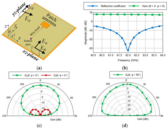
Figure 1.
Wire-bonded patch antenna: (a) simulation model; (b) reflection coefficient and gain; (c) co-polarized and cross-polarized radiation patterns in xz-plane; (d) co-polarized radiation pattern in yz-plane (the cross-polarization pattern in yz-plane is not shown because its values are less than −80 dBi) [43].
The theoretical design was simulated in Altair FEKO using the method of moments. In the model, the feed line of the patch antenna was directly wire-bonded to the pad of the MMIC. The MMIC height was assumed as infinitesimal, and its pad was simulated as a bipolar point source with the source impedance of 50 Ω. Altair FEKO was also used for optimization of the design. The optimization goal was to minimize the reflection coefficient and to maximize the gain in the frequency range from 81 to 83 GHz. Initial dimensions (before optimization) and final dimensions (after optimization) are gathered in Table 2. Major differences are in the width of the microstrip line and the length of the wire bond. The first discrepancy is because narrower microstrip line has larger impedance, which introduces less mismatch between the edge of the patch antenna and the wire bond (the microstrip line operates as the quarter-wave impedance transformer in this circuit). The second one comes from the optimization for the maximum radiation in the broadside direction. The energy radiated by the wire bond could be considered as a loss, but due to the optimization goal defined as a joint minimization of the reflection coefficient and maximization of the gain in the broadside direction, the wire bond length and height were optimized is such a way that the radiated energy improved the broadside gain of the patch antenna (more details are given in [43]). Results of the gain and reflection coefficient simulations are presented in Figure 1b. The −10-dB bandwidth is around 2 GHz, and the maximum gain is 7.8 dBi. Radiation patterns in two orthogonal planes are presented in Figure 1c,d. The latter shows that the radiation of the wire bond increases the gain in the broadside direction, but decreases it for the angle θ in the range between 30° and 60° in yz-plane due to around 180° phase difference between waves radiated by the wire bond and patch antenna.
Table 2.
Dimensions of the wire-bonded patch antenna.
2.2. Experimental Design
The theoretical design presented in the previous section gives a good understanding of the radiating mechanism; however, it is incompatible with standard measurement instruments, which use coaxial or coplanar ground-signal-ground (GSG) interfaces. Therefore, the theoretical design was modified to obtain an experimental design which, after fabrication, could be evaluated experimentally. The main modification comes with adding a 9.55-mm-long coplanar waveguide with ground (CPWG) line to provide an interface for the GSG measurement probe (in case of the reflection coefficient measurements) or the CPWG-to-coax adapter (in case of the radiation pattern measurements). Dimensions of the CPWG line were calculated to achieve the characteristic impedance of 50 Ω. Vias with a diameter of 0.2 mm and spacing of 0.4 mm were added along the edge of the top ground plane surrounding the line to avoid propagation of surface wave in the substrate. Dimensions of the experimental design were reoptimized taking into account many variables, including dimensions of the patch antenna, wire bond, and CPWG line. A photograph of the antenna, fabricated according to obtained experimental design, is presented in Figure 2.
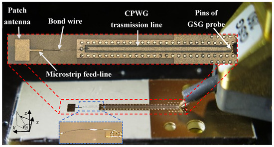
Figure 2.
Photograph of the antenna under reflection coefficient measurements.
2.3. Analysis of Bond Wire Parameters
The wire-bonding process includes many variables, e.g., length, height, and shape of the wire. The following subsection presents the influence of wire bond dimensions on the performance of the experimental design.
2.3.1. Wire Bond Length
Figure 3 shows results of simulations for different wire bond lengths. It can be observed that a half-wavelength wire bond (having a length of 1.83 mm in the free space at 82 GHz, however shorter for the wire bond above the substrate due to the increased effective permittivity) provides fair impedance matching for this structure. Nevertheless, the radiation pattern reveals a destructive interference between the antenna and bond radiation in the broadside direction, resulting in suppressed gain. In contrast, as shown in Figure 4, the bond length extended to full wavelength provides both low reflection coefficient and constructive interference in the broadside direction, thereby yielding high gain values. Thus, the final experimental design involves full-wavelength wire bond connection.
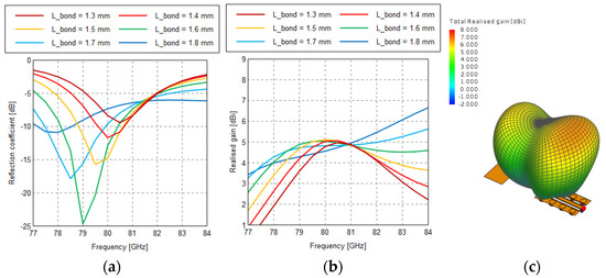
Figure 3.
Simulations of the experimental design having different wire bond lengths around half-wavelength: (a) reflection coefficient; (b) realized gain (reflection loss included), broadside direction; (c) radiation pattern at 80 GHz for the bond length of 1.6 mm.
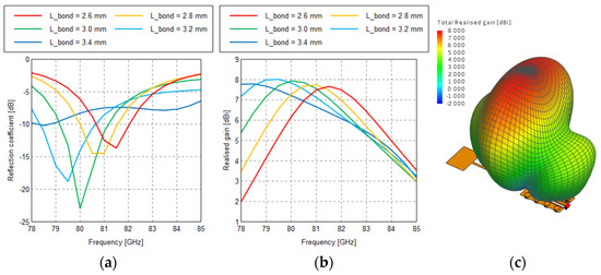
Figure 4.
Simulations of the experimental design having different wire bond lengths around one wavelength: (a) reflection coefficient; (b) realized gain (reflection loss included), broadside direction; (c) radiation pattern at 80 GHz for the bond length of 3.0 mm.
2.3.2. Wire Bond Height
Simulations of different wire bond heights are shown in Figure 5. We can conclude from the results that the wire bond should ideally be as flat as possible.
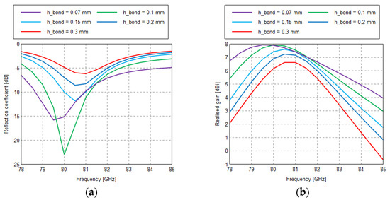
Figure 5.
Simulations of the experimental design having different wire bond heights: (a) reflection coefficient; (b) realized gain (reflection loss included), broadside direction.
2.3.3. Wire Bond Material
Wire bonds used in practice are usually made of aluminum, gold, or copper. All these materials are characterized by a very high conductivity and thus they do not present significant differences in terms of losses. The choice of wire material is usually dictated by technological considerations rather than by their electrical performance. Figure 6 presents simulation results of the antenna equipped with 0.1-mm-high wire bond made of various materials. Differences in reflections coefficient characteristics are negligible (Figure 6a). There is less than 0.1 dB drop in gain for an antenna made with aluminum wire (the most lossy of wires) with respect to the perfect electric conductor (PEC) wire, while differences between aluminum, gold, and copper are less than 0.02 dB (Figure 6b).
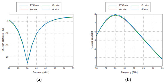
Figure 6.
Simulations of the experimental design for various wire materials: perfect electric conductor (PEC), copper, gold, and aluminum: (a) reflection coefficient; (b) realized gain (reflection loss included), broadside direction.
2.3.4. Wire Bond Thickness
Wire thickness is given as a diameter of its cross section. Figure 7 shows the reflection coefficient for 25 µm, 50 µm, and 70 µm diameters of parabola-shaped wire with the apex at the height of 0.2 mm. The best results are achieved for the thick bond wire with the diameter of 70 µm. This result shows that a higher alignment can be compensated for by using a thicker wire if, due to manufacturing limitations, the wire cannot be very flat.
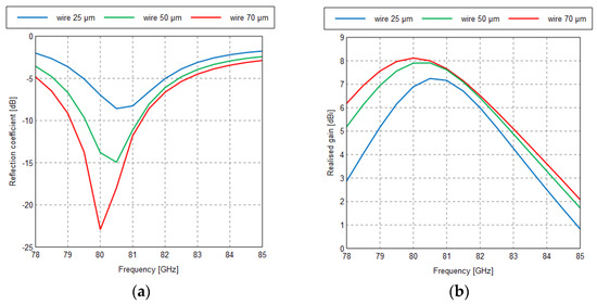
Figure 7.
Simulations of the experimental design for different wire bond diameters: (a) reflection coefficient; (b) realized gain (reflection loss included), broadside direction.
2.3.5. Two Parallel Wire Bonds
The structure was also investigated for two parallel wire bonds with the diameter of 25 μm and the apex at the height of 0.2 mm each. The separation between wires was changing from 50 μm, which is the minimal practically feasible distance [47] to 100 μm, which is only 20 μm less than the microstrip line width. Therefore, wire distances of 50 μm, 70 μm, and 100 μm were examined. Results of simulations presented in Figure 8 show advantageous properties of double wire configuration. It improves slightly when the distance between two wires increases. Comparing the results from Figure 7 and Figure 8, it can be noticed that a thick wire, which is not always possible to use, can be replaced by a double-wire connection.
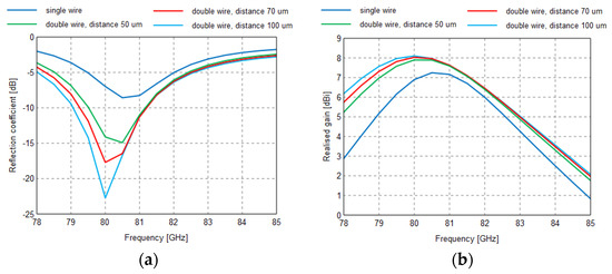
Figure 8.
Simulations of the experimental design for different spacing between two parallel wire bonds: (a) reflection coefficient; (b) realized gain (reflection loss included), broadside direction.
2.3.6. Wire Bond Shape
Bond shape cannot be easily controlled in the manufacturing process, i.e., not every shape is possible. Manufactured samples of the antenna structure showed that the actual shape of the bond wire differs from an ideal parabola. Therefore, another design with real shape of the wire bond was simulated. According to the results presented in Figure 9, the shape plays a substantial role in the performance of the wire-bonded patch antenna. The manual bonding technique used to fabricate the structure does not provide sufficient height control of the long, low-profile bonds to ensure the desired performance. Better results can be expected from automated bonding machines once they have been calibrated. Automatic or semi-automatic wire bonders are very repeatable machines. The main problem is to determine how to set the wire-bonding process parameters to obtain required shape. After parameters of the wire-bonding process are determined, then they can be applied to practical devices on a large scale.
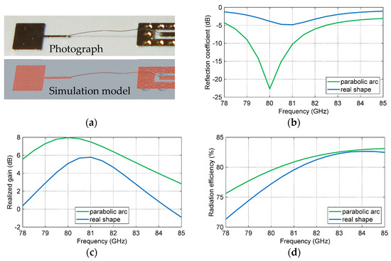
Figure 9.
Simulations of two different wire bond shapes: parabolic arc of 0.1 mm height and real bond shape of 0.23 mm height (a) photograph of the manufactured structure and the model with real bond shape; (b) reflection coefficient; (c) realized gain (reflection loss included), broadside direction; (d) radiation efficiency.
3. Measurement Results
3.1. Fabrication of the Experimental Design
Laminate RO3003G2™ with a thickness of 130 µm and copper cladding of 18 µm was selected as a substrate due to its advantageous electrical parameters; however, its thinness and plasticity complicates the fabrication process. The laminate easily bends and deforms. Its transporting is complicated because special conveyors in machines must be used. Special rigid exit boards must be applied during drilling step, which significantly complicates technological process.
A photolithography technology was used to fabricate the experimental antenna design on the selected laminate. Different stages of fabrication are illustrated in Figure 10. The most important stages of the technological process were as follows:
Figure 10.
Fabrication stages: (a) drilling holes in laminate with phenolic overlays; (b) surface activation and chemical application of copper; (c) application of the photoresist and exposure (ultraviolet light) of mosaic on the photoresist layer; (d) development of the photoresist; (e) galvanic application of the copper layer; (f) galvanic application of the tin layer; (g) photoresist stripping; (h) copper etching; (i) tin stripping; (j) ENIG layer application.
- Drilling of 0.2 mm holes performed on a computer numerical control (CNC) machine with aluminum exit boards instead of phenolic drill exit boards, because the latter turned out to be inappropriate due to swelling debris (Figure 10a).
- A chemical process of dielectric activation for creating a hydrophilic layer on the polytetrafluoroethylene laminate surface (Figure 10b).
- Electroless deposition of a thin copper layer (3~4 μm) over the activated dielectric laminate with Printoganth® P Plus technology by Atotech (Figure 10b).
- Photolithography process which uses ultraviolet light (UV) to make the desired mosaic pattern on the surface of the photoresist including the following:
- Deployment of the KOLON PK1640 photoresist on the top surface of the laminate;
- UV exposure of mosaic on the photoresist layer (Figure 10c); the pattern was exposed on MDI direct imagesetter ST/TT Schmoll;
- Development of the photoresist layer realized with a horizontal line of 1% potassium carbonate solution (Figure 10d).
- Electrochemical deposition of the copper layer (Figure 10e) and the tin layer (Figure 10f) on the exposed copper surface in baths produced by DuPont (Copper Gleam CuPulse and Ronastan EC1, respectively). The copper layer thickness after deposition was 25 µm. The tin layer thickness was 7 μm. The purpose of tin layer deposition is to achieve a metallic resist layer for etching.
- Removal of the photoresist layer after galvanic process using an automatic horizontal line (Figure 10g).
- Etching of the copper (Figure 10h). Tin layer acts as a resist. This process is crucial to obtain the required pattern. Parameters such as pH, temperature, nozzles pressure, and solution density must be precisely controlled in order to achieve sharp copper layer edges. The process was realized using automatic horizontal line with the ammoniacal etching solution produced by MacDermid.
- Tin resist layer removal by using TINSOLV180 produced by Atotech (Figure 10i).
- The last stage was deposition of electroless nickel immersion gold (ENIG) layer (Figure 10j), which creates a solid surface required for the thermosonic wire bonding. Nickel and gold layers were deposited in two baths provided by DuPont–Duraposit™ Electroless Nickel and Aurolectroless™ Immersion Gold, respectively. After the process, the nickel layer thickness was 5 µm and the gold layer thickness was 60 nm.
Photographs of the top layer after the fabrication are presented in Figure 11a,b for the patch antenna and CPWG line, respectively. Figure 11c shows a diagram of the microstrip line cross-section. The dimensions were measured with an optical microscope KEYENSE-VHX-6000 (500x magnification). The etchbacks of the line are 15 μm and 5 μm at the top and bottom surfaces, respectively. These values are acceptable considering that the electromagnetic wave propagates mostly within the substate.
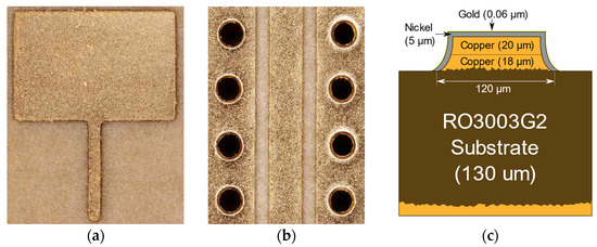
Figure 11.
Fabricated structure (a) photograph of the patch antenna with microstrip feed line; (b) photograph of via holes surrounding the CPWG line; (c) diagram of the cross-section.
Finally, 2.92-mm-long aluminum wire bond with a diameter of 25 µm was added. The antenna after all fabrication stages is presented in Figure 2.
3.2. Reflection Coefficient Measurements
The fabricated antenna was firstly measured for the reflection coefficient. The measurement setup included the Cascade Microtech PM8 EPS200MMW manual probe system with ACP110 GSG probe, Agilent PNA-X N5245A vector network analyzer (VNA), and the Virginia Diodes (VDI) WR-10 (75–110 GHz) waveguide frequency extender. The setup was calibrated using impedance standard substrate with reference plane at the probe’s contact pads.
Results of the measurements compared with the simulated values are shown in Figure 12. As can be noted, only slight detuning of the antenna occurred with a resonant frequency approximately 0.6% higher than simulated.
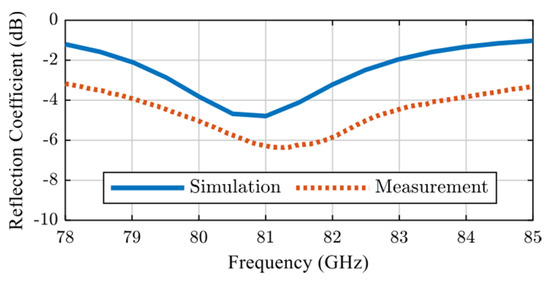
Figure 12.
Reflection coefficient of the experimental design of wire-bonded patch antenna.
3.3. Radiation Pattern Measurements
A different setup was used for radiation pattern measurements. The setup required coaxial connector at the antenna input; therefore, the fabricated structure had to be adapted by attaching a solderless PCB mount connector with 1.00-mm coaxial interface as presented in Figure 13.
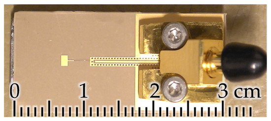
Figure 13.
Wire-bonded patch antenna with a solderless PCB to 1.00-mm coaxial adapter (reference scale in centimeters).
The setup used for the radiation pattern measurement is illustrated in Figure 14. It includes the VNA, two VDI WR-10 waveguide frequency extenders (transmit and receive paths), high-gain reference horn antenna with known characteristics, and a programmable rotary table. One of the frequency extenders is mounted on the rotary table and connected to the fabricated structure with a coaxial cable via a waveguide to the 1.00-mm coaxial adapter.
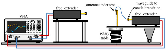
Figure 14.
Radiation pattern measurement setup.
Figure 15 presents a comparison between radiation pattern measurements and simulations. The radiation pattern in xz-plane (Figure 15a) is similar to simulation results. The radiation pattern in yz-plane presented in Figure 15b reveals an influence of the long CPWG transmission line and the adapter, which are significantly larger than dimensions of the wire-bonded patch antenna structure. Fluctuations of the gain in yz-plane are in range of few decibels. Nevertheless, the radiation is still dominant at the broadside direction.
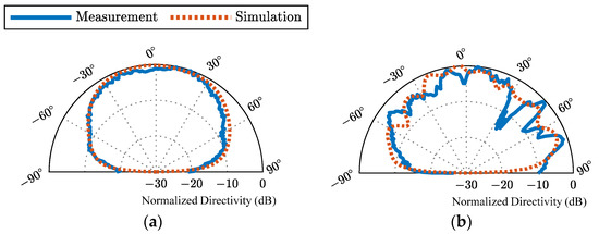
Figure 15.
Radiation pattern measurements (a) xz-plane; (b) yz-plane.
4. Discussion
The application of wire bonds as interconnects in mm-wave devices has been thoroughly investigated in many papers. The general recommendation is to make wire-bonds as short and as flat as possible. Unfortunately, some manufacturing facilities have limitations of the minimum wire bond length and height. Because fabricating relatively long wires (larger than half a wavelength) is easier, this paper analyzed the wire-bonded antenna with an excessively long wire bond. One of the advantages is low reflection loss without implementation of any external matching circuits. Moreover, at the broadside direction the electromagnetic wave radiated by the full-wavelength wire bond is in-phase with the electromagnetic wave radiated by the patch antenna which increases total gain. Therefore, the designed antenna demonstrates a great application potential as a compact antenna structure with broadside radiation and direct connection to the MMIC operating in the mm-wave band. Measurement results revealed that the reflection coefficient is very sensitive to the wire bond shape. Therefore, future work will focus on an analysis of the repeatability of wire bond shapes and proposing shapes which are known to be repeatable with the standard wire-bonding machines.
Author Contributions
Conceptualization, G.B. and Y.Y.; methodology, P.B. and J.S.; investigation, G.B. and P.B.; writing—original draft preparation, G.B.; writing—review and editing, P.B., J.S., J.O. and D.O.; visualization, G.B., J.S. and J.O.; supervision, Y.Y.; project administration, G.B.; funding acquisition, G.B; resources, J.O. and D.O. All authors have read and agreed to the published version of the manuscript.
Funding
This research was funded by the National Science Centre (NCN), Poland in frame of the MINIATURA 4 program under action no. 2020/04/X/ST7/00519. Supported by the Foundation for Polish Science (FNP).
Conflicts of Interest
The authors declare no conflict of interest. The funders had no role in the design of the study; in the collection, analyses, or interpretation of data; in the writing of the manuscript; or in the decision to publish the results.
References
- Baumann, G.; Richter, H.; Baumgaertner, A.; Ferling, D.; Heilig, R.; Hollmann, D.; Mueller, H.; Nechansky, H.; Schlechtweg, M. 51 GHz Frontend with Flip Chip and Wire Bond Interconnections from GaAs MMICs to a Planar Patch Antenna. In Proceedings of the IEEE MTT-S International Microwave Symposium Digest, Orlando, FL, USA, 16–20 May 1995; Volume 3, pp. 1639–1642. [Google Scholar] [CrossRef]
- Heinrich, W.; Hossain, M.; Sinha, S.; Schmuckle, F.-J.; Doerner, R.; Krozer, V.; Weimann, N. Connecting Chips With More Than 100 GHz Bandwidth. IEEE J. Microw. 2021, 1, 364–373. [Google Scholar] [CrossRef]
- Lau, J.H. Recent Advances and Trends in Advanced Packaging. IEEE Trans. Compon. Packag. Manuf. Technol. 2022, 12, 228–252. [Google Scholar] [CrossRef]
- Bajurko, P.; Sobolewski, J.; Bogdan, G.; Godziszewski, K.; Marczewski, J.; Kulawik, J.; Widlok, M.; Yashchyshyn, Y. Millimeter-Wave Transmitter with LTCC Antenna and Silicon Lens. Int. J. Electron. Telecommun. 2022, 68, 269–274. [Google Scholar] [CrossRef]
- Hebeler, J.; Steinweg, L.; Zwick, T. Differential Bondwire Interface for Chip-to-Chip and Chip-to-Antenna Interconnect above 200 GHz. In Proceedings of the 2022 52nd European Microwave Conference (EuMC), Milan, Italy, 27–29 September 2022; Institute of Electrical and Electronics Engineers (IEEE): Piscataway, NJ, USA, 2022; pp. 306–309. [Google Scholar]
- Krems, T.; Haydl, W.; Massler, H.; Ruediger, J. Millimeter-Wave Performance of Chip Interconnections Using Wire Bonding and Flip Chip. In Proceedings of the IEEE MTT-S International Microwave Symposium Digest, San Francisco, CA, USA, 17–21 June 1996; Volume 1, pp. 247–250. [Google Scholar] [CrossRef]
- Valenta, V.; Spreng, T.; Yuan, S.; Winkler, W.; Ziegler, V.; Dancila, D.; Rydberg, A.; Schumacher, H. Design and Experimental Evaluation of Compensated Bondwire Interconnects above 100 GHz. Int. J. Microw. Wirel. Technol. 2015, 7, 261–270. [Google Scholar] [CrossRef]
- SeyyedEsfahlan, M.; Öztürk, E.; Kaynak, M.; Tekin, I. 77-GHz Four-Element Phased-Array Radar Receiver Front End. IEEE Trans. Compon. Packag. Manuf. Technol. 2016, 6, 1162–1173. [Google Scholar] [CrossRef]
- Jiang, C.; Krozer, V.; Bach, H.G.; Mekonnen, G.G.; Johansen, T.K. Broadband Packaging of Photodetectors for 100 Gb/s Ethernet Applications. IEEE Trans. Compon. Packag. Manuf. Technol. 2013, 3, 422–429. [Google Scholar] [CrossRef]
- Fikar, S.; Bogenberger, R.; Scholtz, A.L. A 100GHz Bandwidth Matched Chip to PCB Transition Using Bond Wires for Broadband Matching. In Proceedings of the 12th IEEE Workshop on Signal Propagation on Interconnects (SPI 2008), Avignon, France, 12–15 May 2008. [Google Scholar] [CrossRef]
- Gilardoni, R. Ribbon Bonding for High Frequency Applications Advantages of Ribbon and the Impact on the Microwave Market. In Proceedings of the IMAPS/SEMI Advanced Technology Workshop on Wire Bonding, San Francisco, CA, USA, 2–3 February 2008; p. 5. [Google Scholar]
- Salarpour, M.; Farzaneh, F.; Staszewski, R.B. A Low Cost-Low Loss Broadband Integration of a CMOS Transmitter and Its Antenna for Mm-Wave FMCW Radar Applications. AEU Int. J. Electron. Commun. 2018, 95, 313–325. [Google Scholar] [CrossRef]
- Chu, J.; Li, J.; Zhou, Y.; Cao, J.; Chen, P.; Cao, L. Si-Based System-in-Package Design with Broadband Interconnection for E-Band Applications. IEICE Electron. Express 2021, 18, 20210140. [Google Scholar] [CrossRef]
- Zhang, Y.P.; Sun, M.; Chua, K.M.; Wai, L.L.; Duixian, L. Antenna-in-Package Design for Wirebond Interconnection to Highly Integrated 60-GHz Radios. IEEE Trans. Antennas Propag. 2009, 57, 2842–2852. [Google Scholar] [CrossRef]
- Bondarik, A.; Forsberg, T.; Sjöberg, D.; Sjöland, H.; Tormänen, M. A Bond Wire Connection Implementation at Mm-Wave Active Microstrip Antenna. IEEE Microw. Wirel. Compon. Lett. 2019, 29, 427–429. [Google Scholar] [CrossRef]
- Beer, S.; Ripka, B.; Diebold, S.; Gulan, H.; Rusch, C.; Pahl, P.; Zwick, T. Design and Measurement of Matched Wire Bond and Flip Chip Interconnects for D-Band System-in-Package Applications. In Proceedings of the IEEE MTT-S International Microwave Symposium Digest, Baltimore, MD, USA, 5–10 June 2011. [Google Scholar] [CrossRef]
- Devlin, L. The Future of MM-Wave Packaging. Microw. J. 2014, 57, 24–39. [Google Scholar]
- Cahill, S.S.; Sanjuan, E.A.; Levine, L. Development of 100+ GHz High-Frequency MicroCoax Wire Bonds. In Proceedings of the Proceedings of International Symposium on Microelectronics, San Diego, CA, USA, 29 October–4 November 2006; p. 668. [Google Scholar]
- Bogdan, G.; Yashchyshyn, Y. Study of Bondwire Interconnect for Antenna Applications in W-Band. In Proceedings of the 2021 IEEE International Symposium on Antennas and Propagation and North American Radio Science Meeting (APS/URSI 2021), Singapore, 4–10 December 2021. [Google Scholar] [CrossRef]
- Beer, S.; Rusch, C.; Gottel, B.; Gulan, H.; Zwick, T.; Zwyssig, M.; Kunkel, G. A Self-Compensating 130-GHz Wire Bond Interconnect with 13% Bandwidth. In Proceedings of the IEEE Antennas and Propagation Society, AP-S International Symposium (Digest), Orlando, FL, USA, 7–13 July 2013; pp. 2133–2134. [Google Scholar] [CrossRef]
- Lee, H.Y. Wideband Characterization of a Typical Bonding Wire for Microwave and Millimeter-Wave Integrated Circuits. IEEE Trans. Microw. Theory Tech. 1995, 43, 63–68. [Google Scholar] [CrossRef]
- Ndip, I.; ÖZ, A.; Tschoban, C.; Guttowski, S.; Reichl, H.; Lang, K.D.; Henke, H. Modelling the Shape, Length and Radiation Characteristics of Bond Wire Antennas. IET Microw. Antennas Propag. 2012, 6, 1187–1194. [Google Scholar] [CrossRef]
- Ndip, I.; Becker, K.F.; Brandenburger, F.; Le, T.H.; Huhn, M.; Bauer, J.; Koch, M.; Hempel, M.; Schneider-Ramelow, M.; Lang, K.D. Can Bond Wires Really Be Used as Antennas? In Proceedings of the 2018 7th Electronic System-Integration Technology Conference (ESTC 2018), Dresden, Germany, 18–21 September 2018. [CrossRef]
- Ndip, I.; Lang, K.D.; Reichl, H.; Henke, H. On the Radiation Characteristics of Full-Loop, Half-Loop, and Quasi-Half-Loop Bond Wire Antennas. IEEE Trans. Antennas Propag. 2018, 66, 5672–5686. [Google Scholar] [CrossRef]
- Zhao, B.; Gao, Z.; Tang, M. A Yagi-Uda Array of Bond Wire Antennas with High Front-to-Back Ratio. In Proceedings of the 2021 IEEE International Symposium on Antennas and Propagation and North American Radio Science Meeting (APS/URSI 2021), Singapore, 4–10 December 2021; pp. 1285–1286. [Google Scholar] [CrossRef]
- Bakshi, H.S.; Dong, S.; Momson, I.; Chacon, D.; Chen, Z.; Choi, W.; Blanchard, A.J.; Kenneth, K.O. 180-GHz Broadside Radiation Bond-Wire Antenna for Short-Range Wireless Communication. IEEE Trans. Compon. Packag. Manuf. Technol. 2021, 11, 530–532. [Google Scholar] [CrossRef]
- Shahramian, S.; Baeyens, Y.; Kaneda, N.; Chen, Y.K. A 70-100 GHz Direct-Conversion Transmitter and Receiver Phased Array Chipset Demonstrating 10 Gb/s Wireless Link. IEEE J. Solid-State Circuits 2013, 48, 1113–1125. [Google Scholar] [CrossRef]
- Trzebiatowski, K.; Rzymowski, M.; Kulas, L.; Nyka, K. Simple Millimeter Wave Identification System Based on 60 GHz Van Atta Arrays. Sensors 2022, 22, 9809. [Google Scholar] [CrossRef]
- Jang, T.-H.; Jung, K.P.; Park, C.S. Broadband Millimeter-Wave Antenna in Package with L-Probed E-Shaped Patch Covering 57 GHz to 71 GHz. IEEE Trans. Antennas Propag. 2022, 71, 89. [Google Scholar] [CrossRef]
- Jang, T.; Park, C.S. 60-GHz Wideband L-Probe Circular Slotted E-Shaped Patch Antenna Array. IEEE Access 2022, 10, 79939–79947. [Google Scholar] [CrossRef]
- Anim, K.; Lee, J.N.; Jung, Y.B. High-Gain Millimeter-Wave Patch Array Antenna for Unmanned Aerial Vehicle Application. Sensors 2021, 21, 3914. [Google Scholar] [CrossRef]
- Song, Y.; Wu, Y.; Yang, J.; Tian, Y.; Tong, W.; Chen, Y.; Wang, C.; Tang, X.; Benedikt, J.; Kang, K. A Compact Ka-Band Active Integrated Antenna with a GaAs Amplifier in a Ceramic Package. IEEE Antennas Wirel. Propag. Lett. 2017, 16, 2416–2419. [Google Scholar] [CrossRef]
- Felic, G.; Thomas, C.; Skafidas, E. Design of Co-Planar Waveguide-Fed Slot/Patch Antenna with Wire Bond for a 60-GHz Complementary Metal-Oxide-Semiconductor Transceiver. IET Microw. Antennas Propag. 2011, 5, 490–494. [Google Scholar] [CrossRef]
- Wang, R.; Sun, Y.; Wipf, C.; Scheytt, J.C. An On-Board Differential Patch Array Antenna and Interconnects Design for 60 GHz Applications. In Proceedings of the 2011 IEEE International Conference on Microwaves, Communications, Antennas and Electronic Systems (COMCAS 2011), Tel Aviv, Israel, 7–9 November 2011. [Google Scholar] [CrossRef]
- Zhang, T.; Li, L.; Zhao, D.; Xia, H.; Chai, Y.; Guo, J.; Qian, C.; Zheng, F.C.; Cui, T.J. High-Gain Low-Cost Broadband 60 GHz Differential Integrated Patch Array Antennas with Wire-Bonding Packaging and on-Board Compensation Network. IET Microw. Antennas Propag. 2017, 11, 971–975. [Google Scholar] [CrossRef]
- Felic, G.; Skafidas, E. A CPW-Fed Loop Slot Antenna for Integration with Millimeter Wave CMOS Transceiver. In Proceedings of the 2009 European Wireless Technology Conference, Rome, Italy, 28–29 September 2009; pp. 77–80. [Google Scholar]
- Beer, S.; Rusch, C.; Gulan, H.; Göttel, B.; Girma, M.G.; Hasch, J.; Winkler, W.; Debski, W.; Zwick, T. An Integrated 122-GHz Antenna Array with Wire Bond Compensation for SMT Radar Sensors. IEEE Trans. Antennas Propag. 2013, 61, 5976–5983. [Google Scholar] [CrossRef]
- Simsek, A.; Kim, S.K.; Abdelghany, M.; Ahmed, A.S.H.; Farid, A.A.; Madhow, U.; Rodwell, M.J.W. A 146.7 GHz Transceiver with 5 GBaud Data Transmission Using a Low-Cost Series-Fed Patch Antenna Array through Wirebonding Integration. In Proceedings of the IEEE Radio and Wireless Symposium (RWS), San Antonio, TX, USA, 26–29 January 2020; pp. 68–71. [Google Scholar] [CrossRef]
- Bauer, F.; Wang, X.; Menzel, W.; Stelzer, A. A 79-GHz Radar Sensor in Ltcc Technology Using Grid Array Antennas. IEEE Trans. Microw. Theory Tech. 2013, 61, 2514–2521. [Google Scholar] [CrossRef]
- Yu, J.; Li, X.; Xiao, J. Long-Distance Wireless Mm-Wave Signal Delivery at W-Band. J. Light. Technol. 2016, 34, 661–668. [Google Scholar]
- Fujibayashi, T.; Takeda, Y.; Wang, W.; Yeh, Y.S.; Stapelbroek, W.; Takeuchi, S.; Floyd, B. A 76- to 81-GHz Multi-Channel Radar Transceiver. IEEE J. Solid-State Circuits 2017, 52, 2226–2241. [Google Scholar] [CrossRef]
- Feng, G.; Yi, X.; Meng, F.; Boon, C.C. A W-Band Switch-Less Dicke Receiver for Millimeter-Wave Imaging in 65 Nm CMOS. IEEE Access 2018, 6, 39233–39240. [Google Scholar] [CrossRef]
- Bogdan, G.; Sobolewski, J.; Yashchyshyn, Y. Enhancement of Patch Antenna Gain by Means of Wire Bond Radiation Effect in W Band. In Proceedings of the 2022 24th International Microwave and Radar Conference (MIKON), Gdansk, Poland, 12–14 September 2022; pp. 1–2. [Google Scholar] [CrossRef]
- Rogers Corporation RO3003G2TM Circuit Materials. Available online: https://www.rogerscorp.com/advanced-electronics-solutions/ro3000-series-laminates/ro3003g2-laminates (accessed on 19 January 2023).
- Balanis, C.A. Antenna Theory: Analysis and Design; John Wiley & Sons: Hoboken, NJ, USA, 2016; Volume 4, ISBN 978-1-118-64206-1. [Google Scholar]
- Rabbani, M.S.; Ghafouri-Shiraz, H. Improvement of Microstrip Patch Antenna Gain and Bandwidth at 60 GHz and X Bands for Wireless Applications. IET Microw. Antennas Propag. 2016, 10, 1167–1173. [Google Scholar] [CrossRef]
- Uno, T.; Kitamura, O.; Terashima, S.; Tatsumi, K. 50-Um Fine Pitch Ball Bonding Technology. Nippon. Steel Tech. Rep. 2001, 84, 24–29. [Google Scholar]


Disclaimer/Publisher’s Note: The statements, opinions and data contained in all publications are solely those of the individual author(s) and contributor(s) and not of MDPI and/or the editor(s). MDPI and/or the editor(s) disclaim responsibility for any injury to people or property resulting from any ideas, methods, instructions or products referred to in the content. |
© 2023 by the authors. Licensee MDPI, Basel, Switzerland. This article is an open access article distributed under the terms and conditions of the Creative Commons Attribution (CC BY) license (https://creativecommons.org/licenses/by/4.0/).