Article

Subthreshold Delay Variation Model Considering Transitional Region for Input Slew

1
National ASIC System Engineering Center, Southeast University, Nanjing 210096, China
2
Wuxi Institute of Integrated Circuits Technology, Southeast University, Wuxi 214135, China
3
Shenzhen GWX Technology Co., Ltd., Shenzhen 518000, China
*
Author to whom correspondence should be addressed.
Electronics 2023, 12(3), 615; https://doi.org/10.3390/electronics12030615
Submission received: 21 December 2022 / Revised: 22 January 2023 / Accepted: 24 January 2023 / Published: 26 January 2023
(This article belongs to the Section Computer Science & Engineering)

Abstract

:
Subthreshold design provides the promising advantage of low power consumption at the cost of performance variation and even circuit failure. An accurate and efficient statistical timing model is crucial for timing analysis and performance optimization guidance. Prior works lack the consideration of the impact of slew time or the transitional region for input slew due to process variation and efficient approaches considering the impact of load capacitance and multiple process variations in complex gates, resulting in accuracy loss. In this work, an accurate end efficient gate delay variation model is analytically derived for various input slews and load capacitances. The transitional region between fast and slow input slew is efficiently partitioned with an adaptive error tolerance method so as to characterize timing variation by linear interpolation based on that for fast and slow input slew. In order to consider the impact of load capacitance, the relation between the sensitivity of step delay and the dominant threshold voltage variation is analytically derived. For complex gates, the multiple process variations for both parallel and stacking structures are equivalently expressed by threshold voltage variation from each transistor. The proposed model has been validated under advanced TSMC (Taiwan Semiconductor Manufacturing Company) 12 nm technology at subthreshold region and achieves excellent agreement with Monte Carlo SPICE (Simulation Program with Integrated Circuit Emphasis) simulation results with the max error less than 6.49% for standard deviation of gate delay and 4.63%/6.40% for max/min delay, demonstrating over 4 times precision improvement compared with competitive analytical models.

1. Introduction

Subthreshold design reduces the supply voltage (Vdd) lower than threshold voltage (Vth) for the merits of low power consumption [1,2]. However, it brings the increased sensitivity to process variation, which not only impacts performance but also may lead to hard functional circuit failure [3]. Therefore, an accurate and efficient statistical timing model is crucial for timing analysis and performance optimization guidance in subthreshold regime.
Many research works have been devoted to the subthreshold timing model for gate delay considering process variation [4,5,6,7,8,9,10,11,12,13], which revealed the relation between the delay and the variation sources analytically with physical insights. A fast delay estimation framework via fan-out-4 metric was proposed by [4] to evaluate the max delay variability causing by process variation across multiple PVT (Process-Voltage-Temperature) corners. The subthreshold gate delay model introduced in [5] takes into account the effects of the transient variation during gate switching. An analytical model was derived in [6] based on log-skew-normal distribution to precisely evaluate the gate delay variation as well as the max/min delay. Recently, more attention has been paid to the impact of slew time in delay model. A statistical subthreshold timing model was established in [7] by deriving gate delay variation analytically for the cases of fast and slow input slew separately, which was further optimized in [8] to improve the accuracy near the boundary of fast and slow input slew. Based on the assumption that the gate delay follows lognormal distribution, the statistical gate delay models were established analytically in [9,10] for inverter and complex gates to derive the delay mean value and its standard deviation considering process variations. However, the impact of input slew was not taken into account in these works. In order to reduce the fitting error induced for parameters of current equation, the effective current concept was employed with ad-hoc current points [11,12,13]. The physics-based effective current model for inverter and NAND/NOR gates was derived for near-threshold region with two-dc current points and the corresponding gate delay model was deduced considering variation due to layout dependent effects in [11]. Furthermore, an effective current delay model was presented for inverter with supply-independent threshold points for near-threshold operation in [12] and validated by MC (Monte Carlo) simulation. In [13], the effective current was adopted to approximate the gate delay by the product of the load capacitance and supply voltage over two times the effective current, which was validated for advanced process by comparison to MC simulation results. In spite of the considerable approximation accuracy, the effective current delay modelling approaches were only appropriate for specific input transition time and could not take the influence of input transition time into comprehensive consideration.
It can be seen from prior works that the input slew time and load capacitance pose great challenge to the accuracy of subthreshold delay variation model. However, all of them lack the consideration or over-pessimistically or over-optimistically characterized the delay variation during the transitional region between fast and slow input slew, therefore limit the accuracy and/or applicability of the analytical model for timing analyzers and optimizers. Moreover, few works consider efficient characterization to take the impact of load capacitance and multiple process variations in complex gates into account.
In this work, an accurate and efficient gate delay variation model is proposed for subthreshold region, which was verified under the process of 12 nm technology for multiple logic gates and achieves well agreement with MC SPICE (Simulation Program with Integrated Circuit Emphasis) simulation results with low simulation effort.
The main contribution could be summarized as follows.
  • To increase the model accuracy in the transitional region between fast and slow input slew, the impact of slew time between fast and slow input slew is partitioned efficiently with an adaptive error tolerance method and characterized by linear interpolation.
  • The impact of load capacitance is analytically derived to be independent with the sensitivity of the step delay distribution as well as delay with non-step input slew, so that the variance of gate delay with different load capacitances could be efficiently characterized by scaling the mean of delay with a pre-characterized sensitivity for a reference load.
  • To extend the timing variation model to complex gates, the dominant threshold voltage fluctuation is derived to be equivalent with those in multiple transistors for both parallel and stacking structures.
The rest of this paper is organized as follows. Following the introduction, the timing variation model for inverter is derived in Section 2 considering the impact of input slew and load capacitance. The proposed model is extended to complex gates through threshold voltage fluctuation equivalence in Section 3. The proposed models were validated in Section 4 with the final conclusions drawn in Section 5.

2. Proposed Subthreshold Timing Variation Model for Inverter

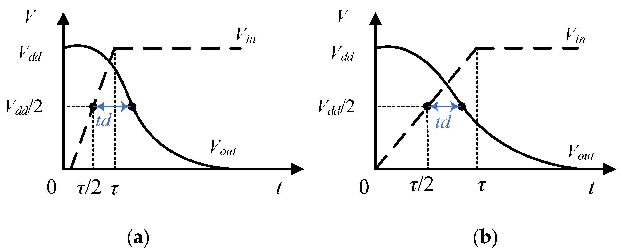
2.1. Timing Variation Model for Fast and Slow Input Slew

The subthreshold drain-source current for NMOS transistor, In, could be represented as Equation (1),
I n = I 0 W L e V g s V t h 0 n V T e λ V d s n V T ( 1 e V d s V T )
where I0 is a process-dependent parameter, W and L are the transistor width and length, Vgs and Vds are gate-source voltage and drain-source voltage, VT is the thermal voltage, λ is the DIBL (Drain Induced Barrier Lowering) coefficient, Vth0 is the threshold voltage with zero bias, and n is the subthreshold slope factor.
Without loss of generality, the output voltage for a rise input of inverter with slew time τ could be derived from Equation (1) to be a piecewise function shown in Equation (2) according to Kirchoff’s current law [5], where CL is the load capacitance.
V o u t ( t ) = { n V T λ ln [ e λ V o u t ( τ ) n V T + I 0 λ e V d d n V T C L n V T W L e V t h 0 n V T ( t τ ) ] ,   t τ n V T λ ln [ I 0 λ τ V d d C L W L e V t h 0 n V T ( e V d d n V T τ t 1 ) + e V d d n V T λ ] ,   0 < t τ
The input waveform for a gate can be classified into two categories with fast and slow slew. As shown in Figure 1a, with a fast input slew, the input voltage increases sharply to Vdd at the time τ before the output voltage decrease to Vdd/2. Correspondingly, with a slow input slew, the input voltage increases tardily to Vdd after the output voltage decrease to Vdd/2 as shown in Figure 1b.
With fast input slew, as shown in Figure 1a, set the second expression Vout = Vdd/2 in Equation (2). The time for the output voltage to reach Vdd/2 can be calculated, expressed as Equation (3),
t V d d / 2 = C L n V T I 0 W L λ e V d d n V T ( e λ V d d 2 n V T e λ V d d n V T ) e V t h 0 n V T + ( 1 n V T V d d ) τ
The gate delay can be calculated by the time difference between the output voltage reaching Vdd/2 and the input voltage reaching Vdd/2 and expressed as Equation (4).
t d = t d 0 + ( 1 2 n V T V d d ) τ
where,
t d 0 = J e V t h 0 n V T ,   J = C L n V T I 0 W L λ e V d d n V T ( e λ V d d 2 n V T e λ V d d n V T )
It can be seen from Equation (4) that the term td0 indicates the gate delay when τ equals zero, i.e., the step delay, which is exponentially proportional with the threshold voltage. The factor J is proportional with CL and inversely proportional with W/L.
For fast input slew, the delay variation can be derived as Equation (5) according to Equation (4), which can be found to be equal to the step delay variation and independent with τ. For specific gate, its step delay variation could be characterized by scaling form a pre-characterized one with CL and W/L. The threshold variation could also be scaled with W/L by Pelgrom’s law [14].
D ( t d ) = D ( t d 0 )
With slow input slew, the gate delay could be derived by Equation (2) when t < τ and expressed as Equation (6).
t d = τ · { n V T V d d ln [ V d d C L I 0 W L λ τ ( e λ V d d 2 n V T e λ V d d n V T ) e V t h 0 n V T ] 1 2 }
According to (6), the gate delay variation could be derived as (7), which is independent with CL and W/L and proportional with threshold variation. The proportional factor is determined by τ and Vdd.
D ( t d ) = ( τ V d d ) 2 D ( V t h 0 )
The derivation of the output voltage in Equation (2) as well as the gate delay in Equations (4) and (6) for fast and slow input is expressed in detail in Appendix A.

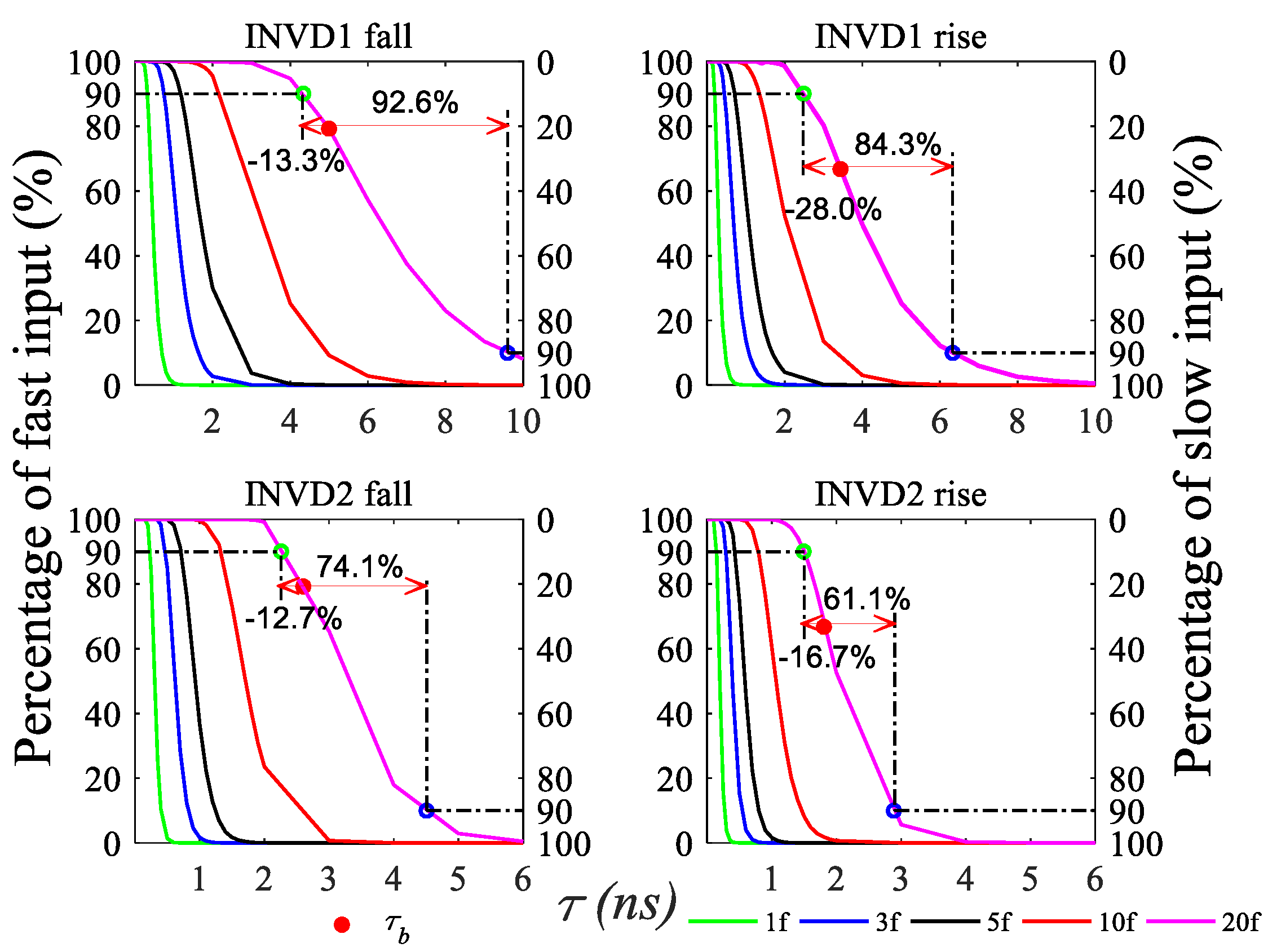
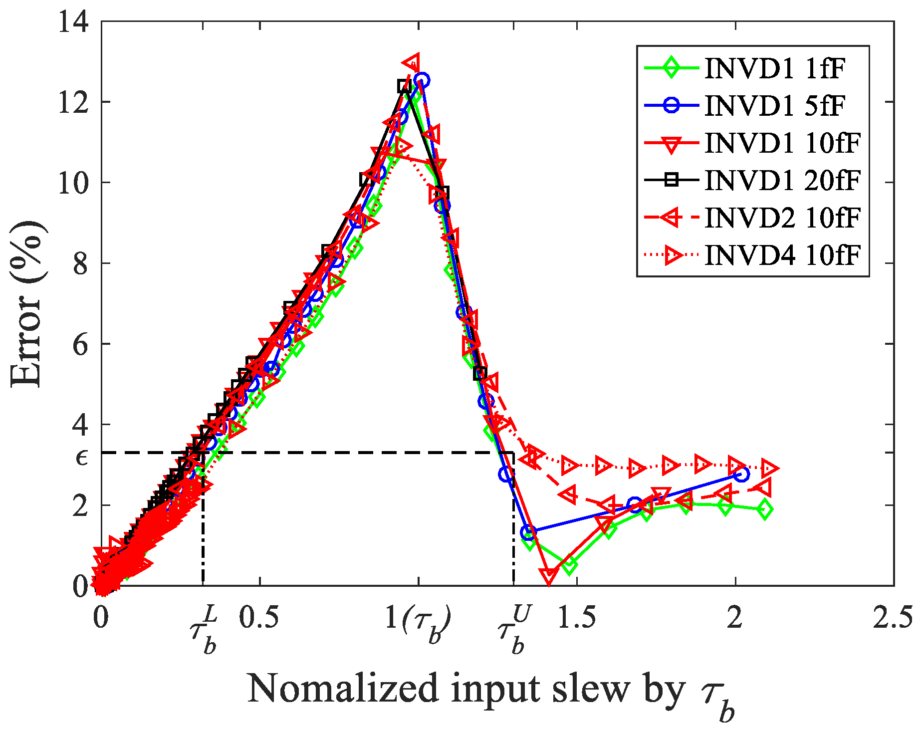
2.2. Timing Variation Model for Input Slew in Transitional Region

The boundary to distinguish fast and slow input slew can be derived with Equation (4) by letting td equals τ/2, as given in Equation (8). It can be seen that τb is proportional to td0 and the proportion factor is independent with CL and W/L.
τ b = V d d n V T t d 0
It should be noted that due to the gate delay variation in subthreshold region, whether the input slew belongs to fast or slow is no longer deterministic. Even a relatively small input slew (τ < τb) may cause the output voltage switch to Vdd/2 earlier than the time τ, or vice versa, which induces the issue that the category of input slew does not switch right at the time τb but through a transitional region around τb. For each specific input slew, the percentages of fast input and slow input within MC SPICE simulations are demonstrated in Figure 2 for inverter with various driver strengths and timing arcs. It can be seen that when the input slew equals zero, it is verified to be fast input for 100% of MC simulation results. As it increases, partial of them turns out to be slow, leading to a nonneglectable transitional region around the deterministic boundary for fast and slow input slew. If defining the transitional region as the region between 90% fast input and 10% fast input, i.e., 90% slow input, it can be seen from Figure 2 that it may cover up to −28.0%~92.6% range around τb, which expands with smaller driver strength and larger load capacitance. When τ falls in the transitional region, both the model for fast and slow input slew are no longer valid, suffering from significant accuracy loss.
Although the range of transitional region varies with load capacitance and the gate itself, it could be investigated that the relation between the range of transitional region and τb is independent with τ and CL so that the transitional region could be partitioned adaptively. Figure 3 shows the error of the proposed delay variation models for fast and slow input slew by comparing with MC simulation results. It can be seen that the error peaks at τb and decreases linearly with τ around τb with a consistent slope for all cases. Therefore, by defining a tolerable error ε (e.g., 3%), the upper and lower boundaries of the transitional region could be adaptively restricted between τ b L and τ b U , which could be set with two factors, θL(ε) and θH(ε), for the corresponding τb as shown in Equation (9).
{ τ b L = ( 1 θ L ( ε ) ) τ b τ b U = ( 1 + θ U ( ε ) ) τ b
Based on the tolerable error-adaptive boundary factors, θL(ε) and θH(ε), the delay variation model for transitional region could be analytically derived as the linear interpolation based on the model for fast and slow input slew, thus the analytical model for transitional region could be represented as Equation (10).
D ( t d ) = [ D ( t d 0 ) + ( τ τ b L ) D ( t d ) | τ b H D ( t d ) | τ b L τ b H τ b L ] 2
where D ( t d ) | τ b H and D ( t d ) | τ b L are the delay variations at τ b L and τ b U by Equations (5) and (7), respectively.

2.3. Timing Variation Model for Different Loads

Although the inverter delay could be analytically represented with the step delay at different input slews, it should be noted the step delay is dependent with the load capacitance, whose impact should be considered in the timing variation model. As can be seen from Equation (4), due to the predominant normally distributed threshold voltage fluctuation at subthreshold voltage region [5,6], the step delay follows a log-normal distribution with the sensitivity, σ ( t d 0 ) / μ ( t d 0 ) , derived as Equation (11), where σ ( V t h 0 ) denotes the standard deviation of threshold voltage. It can be seen that the sensitivity of step delay is independent with load capacitance, therefore the standard deviation of step delay could be characterized as the sensitivity for a reference load, e.g., 1 fF, and increases linearly with the mean of step delay as shown in Equation (12).
σ ( t d 0 ) μ ( t d 0 ) = σ ( V t h 0 ) n V T
σ ( t d 0 ) = σ ( t d 0 ) μ ( t d 0 ) | r e f μ ( t d 0 )
Figure 4 verifies the accuracy of Equation (12) for different gates and driver strengths. As the mean of gate step delay increases, the standard deviation increases with the slope of σ ( t d 0 ) μ ( t d 0 ) | r e f and fits the simulation results well. For driver strengths including D1, D2 and D4, the standard deviation of step delay demonstrates different increase slope. It is worth noting that although the relation between the sensitivity of step delay and the standard deviation of threshold voltage is derived based on inverter, it could be found in Figure 4 that Equation (12) is also appropriate for complex gates such as NAND and NOR gates, which provides an efficient approach to build the timing variation model for different loads.
So far, a statistical delay model of inverter in different input slew and load capacitances has been established.

3. Proposed Subthreshold Timing Variation Model for Complex Gates

According to Section 2, the variance of gate delay is dominantly affected by threshold voltage fluctuations. Compared with the inverter, the statistical delay model of the complex gate has multiple threshold voltage fluctuations, whose structures include parallel structure and stacking structure. As shown in Figure 5, the pullup network of NAND and the pulldown network of NOR are structed in parallel while the pulldown network of NAND and the pullup network of NOR are structed in stacking. For parallel structure, the current distribution is the sum of current from each single transistor while for stacking structure, the current for each transistor is equal but is affected by different drain-source voltage. The current fluctuations for both structures are determined by multiple threshold voltage fluctuations. In this section, the issue of threshold voltage equivalence for multiple transistors is studied for both structures so that the timing variation model could be extended to complex gates.

3.1. Threshold Voltage Equivalence for Parallel Structure

By taking the parallel structure of two-input NOR gate as an example, the variance of current in each transistor, Isingle, could be derived to be Equation (13) according to Equation (1).
D ( I s i n g l e ) = I s i n g l e 2 n V T D ( V t h 0 )
Since the current of each transistor in parallel structure follows an independent identicall distribution, the variance of currrent for parallel structure, Ipara, could be expressed as the sum of the variance of currents from each transistor in Equation (14).
D ( I p a r a ) = 2 D ( I s i n g l e ) = I s i n g l e 2 n V T 2 D ( V t h 0 )
According to Equations (13) and (14), the equivalent threshold voltage variance of the parallel structure for two-input gate could be expressed as Equation (15),
D ( V t h 0 p a r a ) = 1 2 D ( V t h 0 )

3.2. Threshold Voltage Equivalence for Stacking Structure

In the stacking structure, the transistors are connected seriesly and charges or discharges with an identicial current. By taking the stacking structue in the two-input NAND gate as an example, the current of upper and lower transistor, IU and IL, could be expressed as Equation (16) by denoting the voltage at the intermediate conntected node as VX.
{ I U = I 0 W L e V D D V X V t h 0 n V T e λ V D D V X n V T ( 1 e V D D V X V T ) I L = I 0 W L e V D D V t h 0 n V T e λ V X n V T ( 1 e V X V T )
Accoding to Equation (16), the variance of both IU and IL could be derived as Equation (17).
{ D ( I U ) = I U 2 n V T D ( V t h 0 ) D ( I L ) = I L 2 n V T D ( V t h 0 )
Since IU and IL are equal and the threshold voltages of both transistors follow independent identical distribution, the equivalent threshold voltage variance of the stacking structure could be proved to be identical with variance of threshold voltage of each transistor and expressed as (18).
D ( V t h 0 s t a c k ) = D ( V t h 0 )
Thus, with the equivalent threshold voltage variances expressed in Equations (15) and (18), the subthreshold timing variation model proposed in Section 2 for inverter could be extended for complex gates with parallel structure and stacking structure.

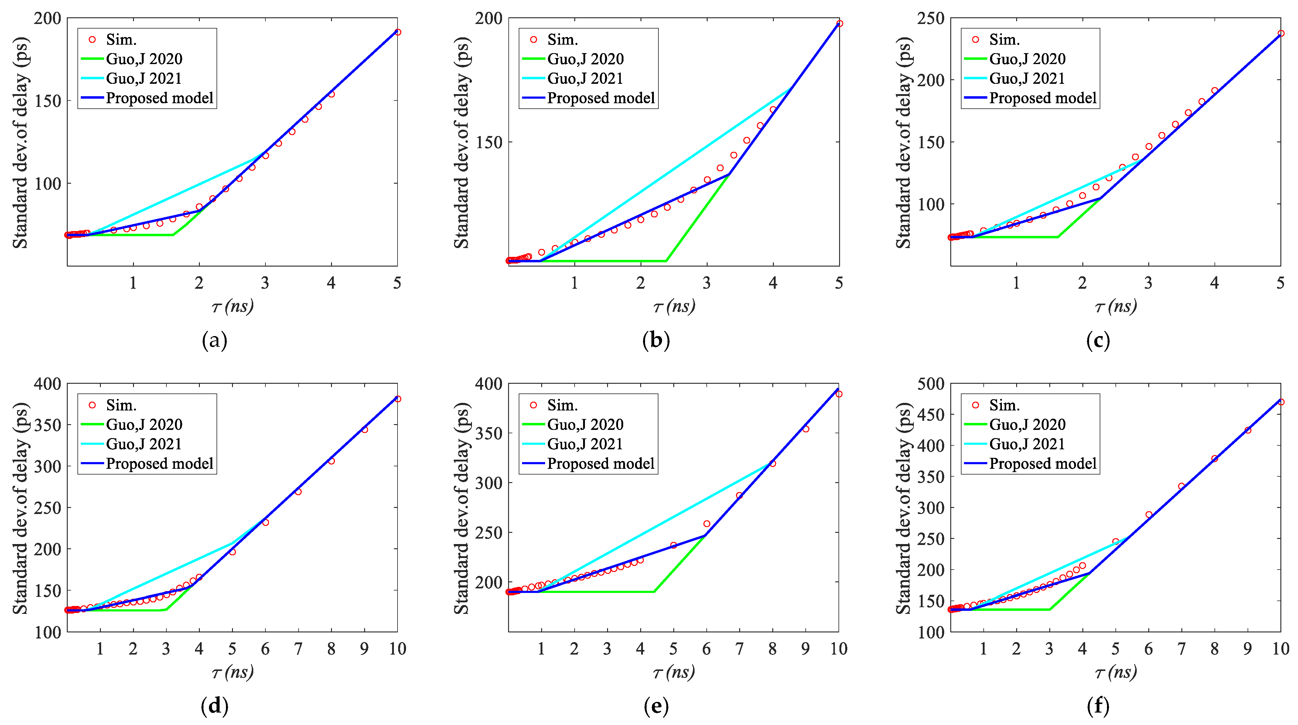
4. Experimental Results and Discussions

In order to validate the proposed delay variation model, it was realized in MATLAB and applied under TSMC (Taiwan Semiconductor Manufacturing Company) 12 nm technology at a subthreshold voltage, 0.3 V, and compared with MC SPICE simulation results and competitive models.
As shown in Figure 6, the standard deviation of gate delay by the proposed model achieves excellent agreement with MC SPICE simulation results for inverter, NAND and NOR gates. It is worth noting that besides the satisfying precision for fast and slow input slews, the proposed model keeps consistent with MC SPCIE simulation results in transitional region owing to the partition method with adaptive error tolerance and the derived model for this region. The competitive model from [7] neglects the statistical impact to the boundary between the fast and slow input slew, resulting in over-optimistic estimation for delay variation. As for [8], the transitional region is considered to be across the 3σ region of gate delay around τb, leading to over-pessimistic estimation. Figure 7 shows the error results of different models of INV 5 fF. It can be seen from the figure that the maximum error of model in [7] and [8] is, respectively, 12% and 18% while the maximum error of proposed model is less than 3%. Compared with the prior methods, our model achieves over 4 times precision improvement.
Table 1, Table 2 and Table 3 illustrate the error of the proposed timing variation model for the standard deviation of logic gates including INV, NAND and NOR with different input slews and load capacitances. For different transition time, loads and structures, the maximum error of the proposed model is less than 4.15%, 5.21% and 6.49% for INV, NAND and NOR gates, respectively.
Compared with MC SPICE simulation results, the error of the max/min inverter delays at the ±3σ percentile points with the proposed model are listed in Table 4 and Table 5. It can be seen that for various load capacitances, the maximum error with fast and slow input slew are less than 5.78% and 6.40%, respectively, while in the transitional region, the error for the max/min gate delay is up to 4.89%.

5. Conclusions

The impact of input slew poses great challenge to characterize the gate delay variation in subthreshold region. This paper establishes an accurate and efficient delay variation model by adaptively partitioning the transitional region of input slew and analytically deriving with linear interpolation knob. Firstly, we propose the corresponding delay variation model for input transition region based on the models for fast input and slow input. Secondly, the step delay variation model for different load capacitances is established. Finally, the proposed delay model is extended to complex gates. The proposed delay model can be used in any input slew, load capacitance and different complex gates. Compared with the previous work, the proposed delay model can significantly improve the accuracy and reduce the simulation cost.

Author Contributions

P.C., Y.W. (Yu Wang) and W.X. organized this work. W.X., Y.W. (Yuanjie Wu) and W.L. performed the modeling, simulation and experiment work. The manuscript was written by P.C. and W.X., and edited by W.X. All authors have read and agreed to the published version of the manuscript.

Funding

This work was supported in part by the National Key Research and Development Program of China (Grant No. 2019YFB2205004), and in part by the National Natural Science Foundation of China under Grant (62174031) and in part by the Jiangsu Natural Science Foundation (Grant No. BK20201233) and in part by the SEU-SMIT EDA Joint Laboratory Project.

Acknowledgments

The authors thank to Xinming Liu for providing technical support.

Conflicts of Interest

The authors declare no conflict of interest.

Appendix A

For an inveter with rise input with slew time τ and load capacitance CL, the relation between the output voltage, Vout, and the current of NMOS/PMOS transistor, In/Ip, could be expressed as (19) according to Kirchhoff’s current law. Since the subthreshold PMOS current is significantly smaller than the NMOS current, it could be neglected [6,9,11,12].
I n I p = C L d V o u t d t
By integrating over time t and considering that the output voltages fall from the supply voltage Vdd, the expression of the output voltage can be obtained.
0 t I n d t = V d d V o u t C L d V o u t
During the input rise of inverter, the current Ids could be expressed as a piecewise function in for the time before and after τ according to the expression shown in (21) of the manuscript so that the output voltage could be derived accordingly.
I n = { I 0 W L e V d d t / τ V t h 0 n V T e λ V d s n V T ( 1 e V d s V T ) , 0 < t τ I 0 W L e V d d V t h 0 n V T e λ V d s n V T ( 1 e V d s V T ) , t > τ
(1)
0 < tτ
During this time interval, the input voltage rises from 0 to Vdd while the output voltage falls from Vdd to Vout(τ). By substituting Ids with Equation (21), the expression of Equation (20) is written as Equation (22). Considering that Vds is far higher than VT during this interval, the term 1 e V d d V T is approximated as one here.
0 t I 0 W L e V d d t / τ V t h 0 n V T e λ V o u t ( t ) n V T d t = V d d V o u t ( t ) C L d V o u t
Therefore the expression of output voltage can be obtained through integral operation as shown in Equation (23).
V o u t ( t ) = n V T λ ln [ I 0 λ τ V d d C L W L e V t h 0 n V T ( e V d d n V T τ t 1 ) + e V d d n V T λ ]
(2)
t > τ
During this time interval, the input voltage remains to be Vdd while the output voltage continues to fall from Vout(τ). By substituting Ids with Equation (21), the expression of Equation (20) is written as Equation (24).
τ t I 0 W L e V d d V t h 0 n V T e λ V o u t ( t ) n V T d t = V o u t ( τ ) V o u t ( t ) C L d V o u t
Therefore the expression of output voltage can be obtained through integral operation as shown in Equation (25).
V o u t ( t ) = n V T λ ln [ e λ V o u t ( τ ) n V T + I 0 λ e V d d n V T C L n V T W L e V t h 0 n V T ( t τ ) ]
Combining Equations (23) and (25), the expression of Equation (2) in the manuscript for the output voltage is derived.
With fast input slew, the gate delay could be derived by letting the output voltage to be Vdd/2 in Equation (25) and expressed as Equation (3) in the manuscript, which could be written as (4) to be proportional with the input slew, τ, based on the step delay, td0.
With slow input slew, the gate delay could be derived by letting the output voltage to be Vdd/2 in Equation (23) and expressed as Equation (6) in the manuscript.

References

  1. Pinckney, N.; Blaauw, D.; Sylvester, D. Low-power near-threshold design: Techniques to improve energy efficiency energy-efficient near-threshold design has been proposed to increase energy efficiency across a wid. IEEE Solid State Circuits Mag. 2015, 7, 49–57. [Google Scholar] [CrossRef]
  2. Alioto, M. Ultra-Low Power VLSI Circuit Design Demystified and Explained: A Tutorial. IEEE Trans. Circuits Syst. I Regul. Pap. 2012, 59, 3–29. [Google Scholar] [CrossRef]
  3. Dreslinski, R.G.; Wieckowski, M.; Blaauw, D.; Sylvester, D.; Mudge, T.N. Near-Threshold Computing: Reclaiming Moore’s Law Through Energy Efficient Integrated Circuits. Proc. IEEE 2010, 98, 253–266. [Google Scholar] [CrossRef]
  4. Alioto, M.; Scotti, G.; Trifiletti, A. A novel framework to estimate the path delay variability on the back of an envelope via the fan-out-of-4 metric. IEEE Trans. Circuits Syst. I Regul. Pap. 2017, 64, 2073–2085. [Google Scholar] [CrossRef]
  5. Corsonello, P.; Frustaci, F.; Lanuzza, M.; Perri, S. Over/undershooting effects in accurate buffer delay model for sub-threshold domain. IEEE Trans. Circuits Syst. I Regul. Pap. 2014, 61, 1456–1464. [Google Scholar] [CrossRef]
  6. Cao, P.; Liu, Z.; Guo, J.; Wu, J. An Analytical Gate Delay Model in Near/Subthreshold Domain Considering Process Variation. IEEE Access 2019, 7, 171515–171524. [Google Scholar] [CrossRef]
  7. Guo, J.; Cao, P.; Li, M.; Liu, Z.; Yang, J. Statistical Timing Model for Subthreshold Circuit with Correlated Variation Consideration. In Proceedings of the 2020 IEEE International Symposium on Circuits and Systems (ISCAS), Seville, Spain, 12–14 October 2020; pp. 1–5. [Google Scholar]
  8. Guo, J.; Cao, P.; Li, M.; Gong, Y.; Liu, Z.; Bai, G.; Yang, J. Semi-Analytical Path Delay Variation Model With Adjacent Gates Decorrelation for Subthreshold Circuits. IEEE Trans. Comput. Aided Des. Integr. Circuits Syst. 2021, 40, 931–944. [Google Scholar] [CrossRef]
  9. Frustaci, F.; Corsonello, P.; Perri, S. Analytical delay model considering variability effects in subthreshold domain. IEEE Trans. Circuits Syst. II Express Briefs 2012, 59, 168–172. [Google Scholar] [CrossRef]
  10. Shiomi, J.; Ishihara, T.; Onodera, H. Microarchitectural-level statistical timing models for near-threshold circuit design. In Proceedings of the 20th Asia and South Pacific Design Automation Conference, Tokyo, Japan, 19–22 January 2015; pp. 87–93. [Google Scholar]
  11. Sharma, A.; Alam, N.; Bulusu, A. Effective Drive Current for Near-Threshold CMOS Circuits’ Performance Evaluation: Modeling to Circuit Design Techniques. IEEE Trans. Electron Devices 2018, 65, 2413–2421. [Google Scholar] [CrossRef]
  12. Dani, L.M.; Mishra, N.; Sharma, A.; Bulusu, A. Variation-Aware Prediction of Circuit Performance in Near-Threshold Regime Using Supply-Independent Transition Threshold Points. IEEE Trans. Electron Devices 2019, 66, 5065–5071. [Google Scholar] [CrossRef]
  13. Pidin, S. Influence of Within-Die Transistor Characteristics Variation on FINFET Circuit Delay. IEEE Trans. Electron Devices 2021, 68, 3276–3282. [Google Scholar] [CrossRef]
  14. Pelgrom, M.J.M.; Duinmaijer, A.C.J.; Welbers, A.P.G. Matching properties of MOS transistors. IEEE J. Solid-State Circuits 1989, 24, 1433–1439. [Google Scholar] [CrossRef]
Figure 1. Gate delay td induced by input slew τ. (a) fast input; (b) slow input.
Electronics 12 00615 g001
Figure 2. Transition procedure of fast/slow input slew due to process variation.
Electronics 12 00615 g002
Figure 3. Error of the proposed delay variation model with normalized τ.
Electronics 12 00615 g003
Figure 4. Verification of step delay variation model for different loads by simulation results for (a) inverter, (b) NAND gate and (c) NOR gate.
Electronics 12 00615 g004
Figure 5. Parallel structure and stacking structure for (a) NAND gate and (b) NOR gate.
Electronics 12 00615 g005
Figure 6. Verification results of the proposed and competitive models [7,8] compared with MC SPICE simulation results. (a) inverter gate with 5 fF load; (b) NAND gate with 5 fF load (c) NOR gate with 5 fF load. (d) inverter gate with 10 fF load; (e) NAND gate with 10 fF load (f) NOR gate with 10 fF load.
Electronics 12 00615 g006
Figure 7. Model error comparison with [7,8] for inverter delay with load 5 fF.
Electronics 12 00615 g007
Table 1. Standard deviation error with the proposed model for INV (%).
Slew100 ps500 ps1 ns2 ns3 ns5 ns
Load
1 fF1.554.151.680.090.623.1
3 fF0.270.063.843.291.440.56
5 fF0.590.582.192.522.691.44
10 fF0.17 1.561.071.831.642.99
20 fF0.64 0.89 1.74 3.77 0.72 3.37
Table 2. Standard deviation error with the proposed model for NAND (%).
Slew100 ps500 ps1 ns2 ns3 ns5 ns
Load
1 fF1.02 1.92 0.26 1.45 0.17 0.33
3 fF0.28 4.36 2.94 0.32 4.63 2.78
5 fF0.06 2.93 4.67 1.78 0.16 5.21
10 fF0.15 1.75 3.43 4.12 2.12 2.20
20 fF0.28 1.15 1.96 3.39 4.94 2.46
Table 3. Standard deviation error with the proposed model for NOR (%).
Slew100 ps500 ps1 ns2 ns3 ns5 ns
Load
1 fF0.35 6.49 1.00 0.65 1.29 3.26
3 fF0.29 6.26 5.55 0.71 2.25 3.12
5 fF0.36 6.30 5.02 6.01 1.35 3.19
10 fF0.44 3.43 6.41 4.15 4.90 1.08
20 fF0.53 2.01 3.39 6.40 4.72 3.47
Table 4. Error of max inverter delay at 3σ percentile point (%).
LoadFast InputTransition AreaSlow Input
MaxAveMaxAveMaxAve
5 fF4.463.964.533.032.972.95
10 fF4.504.074.573.732.672.24
20 fF4.153.554.634.282.862.08
Table 5. Error of min inverter delay at −3σ percentile point (%).
LoadFast InputTransition AreaSlow Input
MaxAveMaxAveMaxAve
5 fF4.283.824.222.756.404.73
10 fF5.784.594.403.275.764.86
20 fF4.573.904.894.253.562.94
Disclaimer/Publisher’s Note: The statements, opinions and data contained in all publications are solely those of the individual author(s) and contributor(s) and not of MDPI and/or the editor(s). MDPI and/or the editor(s) disclaim responsibility for any injury to people or property resulting from any ideas, methods, instructions or products referred to in the content.

