1. Introduction
Recent development in Wireless Power Transfer (WPT) and Inductive Power transfer (IPT) makes it a suitable replacement for wired charging, without much compromise. The wireless power transfer is usually used for battery charging [
1,
2]. The WPT systems are scalable, which allows the transfer of a wide range of power to different devices. The system can transfer power from a couple of watts to a couple of kilowatts. The low power range is usually used for the charging of medical implants [
3,
4], mobile phones, wireless headphones, and smart watches [
5,
6,
7]. The medium range can be used for charging of laptops. Finally, the kilowatt range can be used for the charging of electric vehicles [
8,
9,
10].
The IPT system transfers energy wirelessly via a high frequency magnetic field. Usually, the IPT system consists of one transmitter and one receiver coil, separated by an air gap. The coils form a transformer with a large air gap. Compared to the wired energy transfer, wireless energy transfer has lower overall efficiency, which is highly dependent on the physical position of the receiver to the transmitter. The efficiency of the IPT system is dependent on the coupling coefficient between the transmitter and the receiver coil. The coupling coefficient decreases with the increase of distance between the transmitter and the receiver coil. However, the distance is usually based on the application and does not change. On the other hand, there is always the possibility of misalignment between the transmitter and the receiver, which also decreases the coupling coefficient, and therefore decreases the efficiency of the system. The misalignment tolerance can be increased by optimizing the transmitter and the receiver coils and by switching to different coil types. Misalignment tolerance can be increased by using bipolar transfer coil structures with a directional magnetic field. One of the coils with a directional magnetic field is the DD coil [
11].
The main advantage of the so-called bipolar DD coils is better tolerance to misalignment in one of two horizontal directions. Therefore, DD coils are especially usable for applications with a higher possibility of misalignment. However, due to the directional magnetic field, the coils are not tolerant to the z axis rotation between the transmitter and the receiver. If the transmitter and receiver DD coils are perpendicular to each other, the coupling coefficient between the coils is reduced to zero. Therefore, DD coils should only be used in applications where there is no rotation between the transmitter and receiver, for instance electric vehicle charging.
This paper presents a solution to how to implement the transmitter and the receiver coil structure with a directional magnetic field and tolerance to rotation between the transmitter and the receiver. Both the transmitter and the receiver coil consist of two DD coils in a double DD coil structure [
12]. A system using the double DD coil structure has larger power density, symmetrical misalignment tolerance, and is also the basis for the rotationally tolerant IPT system. The main disadvantage of the system using single DD coils can be eliminated using the double DD coil structure. If the transmitter and the receiver double DD coil are not rotated to one another, only the DD1 transmitter and DD1 receiver coil are coupled. The same goes for the DD2 transmitter and the receiver coil. However, if the additional rotation is introduced between the transmitter and the receiver double DD coil, the DD1 transmitter coil is coupled to DD1 and DD2 receiver coil. Same goes for DD2 transmitter coil. This enables rotation tolerant IPT systems, however, the system cannot be studied as two separate IPT systems, as presented in [
13]. Therefore, a new dynamic model should be derived.
This article is organized as follows. The second chapter, after the introduction, describes double DD coils and an IPT system using a double DD coil structure. The third chapter presents a reduced model of the IPT system using a double DD coil structure, when there is a rotation between the transmitter and the receiver coil. The PI control structure and the control design is presented in chapter four. The fifth chapter presents the results of the successfully implemented control on the low-power, small scale experimental system. Finally, chapters six and seven serve as a discussion and conclusion of the paper.
2. Wireless Power Transfer Using DD Coil Structure
The bipolar DD coil was first introduced in [
11] as a suitable alternative to the planar spiral coils. The coil consists of two spiral D coils, connected in series. The DD coils generate a directional magnetic field, similar to other bipolar coils, such as a flux pipe. The main advantage of the DD coil is low thickness and misalignment tolerance in one of the directions. The most tolerant direction is perpendicular to the generated magnetic flux. The coil is less tolerant to misalignment in the direction of the generated magnetic flux. Therefore, the misalignment tolerance of a DD coil is highly asymmetrical.
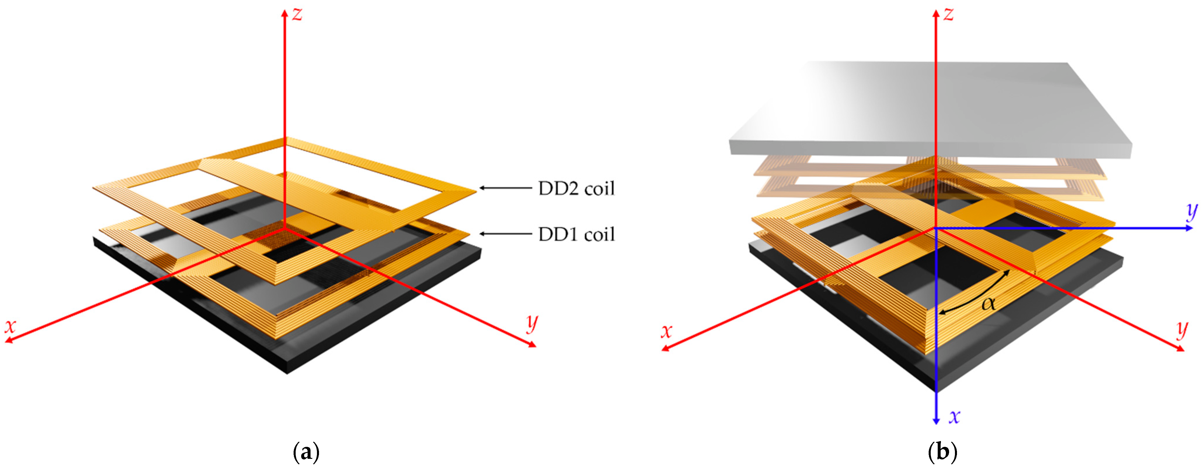
A single DD coil can be upgraded into a double DD coil structure, as presented in
Figure 1a. The structure consists of two DD coils, named the DD1 and DD2 coils. The DD1 coil is the bottom coil, positioned directly on a ferrite tile, and the DD2 coil is placed on top of the DD1 coil. The DD1 and DD2 coils are perpendicular to one another. Because DD coils are dependent on rotation the DD1 and DD2 coils are not magnetically coupled, and the coupling coefficient between the coils is approximately zero. The DD1 can be excited separately from the DD2 coil.
If the transmitter and receiver double DD coil are not rotated to one another, as presented in [
12], the energy is transferred via two independent channels. This results in higher power density. The DD1 coil on the transmitter coil is coupled only to the DD1 receiver coil, and the DD2 transmitter coil is coupled to the DD2 receiver coil. The pair of DD1 and DD2 coils do not interact.
On the other hand, the receiver coil can be rotated to the transmitter coil, as presented in
Figure 1b. The angle of rotation is marked with
α. The coils are not rotated to each other if
α is 0°. When
α is greater than 0°, the DD1 transmitter coil is coupled to the DD1 and DD2 receiver coils. The same is true for the DD2 transmitter coil, which is also connected to the DD1 and DD2 receiver coils. The DD1 and DD2 coils on the transmitter and the receiver coil are still not coupled. The additional coupling complicates the mathematical model of the system by introducing an additional DD cross coupling, which is dependent on α.
The output load voltage is also highly dependent on the rotation between the transmitter and the receiver coil. Therefore, control is required of the IPT system. The main purpose of the control is stabilizing the output voltage and compensating the influence of the load change and change in the coupling coefficient.
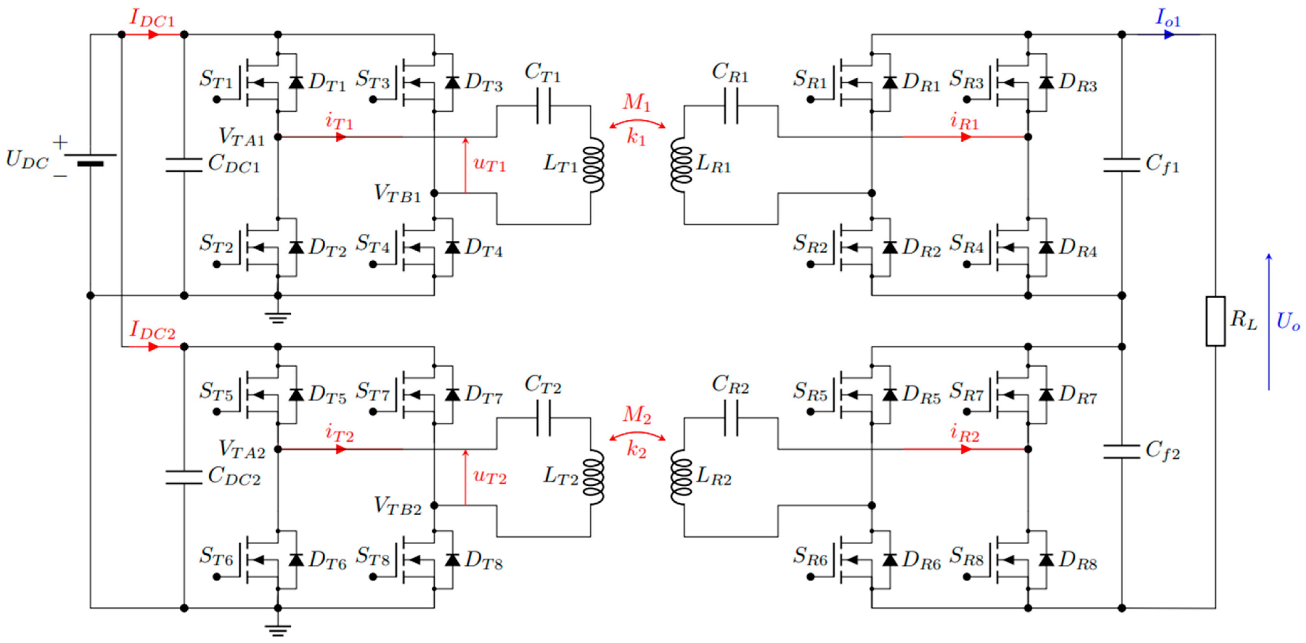
The basic circuit of the IPT system using a double DD coil is presented in
Figure 2. The presented IPT system uses series-series (SS) compensation. The main advantage of an SS compensation scheme is that the resonant frequency is constant, and not dependent on the coupling coefficient and resistance of the load [
14]. In the case of rotation of the double DD transmitter receiver coils, the coupling coefficient changes.
The DD coils with compensation capacitors form a resonator circuit with band pass properties. The DD1 and DD2 transmitter coils are excited separately. The DD1 transmitter coil is excited by the first full bridge inverter using voltage uT1. The DD2 transmitter coil is connected to the second full bridge inverter and excited with voltage uT2. Both high-frequency inverters are connected to the DC source UDC.
The receiver side consists of two full bridge synchronous rectifiers connected to the single load. In practical applications of the IPT systems, the load is usually an additional DC/DC converter or the battery. During the charging process, the equivalent resistance of the load changes. In our case, we replaced load with fixed value resistor RL. Each of the receiver coils is connected to one of the rectifiers. The output voltage Uo is the sum of Uo1 and Uo2, which are the voltages at the output of each rectifier. The output voltage can be controlled by controlling the current through the transmitter coil, and by controlling the excitation voltage. The most common way of controlling the high-frequency inverter is using modulation with a phase shift, which influences the first harmonic component of the excitation voltage.
On the other hand, the system can be controlled by switching the frequency generated by the high-frequency inverters. Because the IPT system behaves as a band-pass filter, the change in frequency also changes the excitation current. The resonant frequency of the system can be calculated using:
where
fs1 and
fs2 are the resonant frequencies of the DD1 and DD2 parts of the system.
LT1 and
LR1 are the self-inductances of the DD1 and DD2 receiver coils, and
CT1 and
CR1 are the compensation capacitors on the transmitter and the receiver side.
LT2 and
LR2 are the self-inductances of the DD2 transmitter and the receiver coils, and
CT2 and
CR2 are the compensation capacitors on the transmitter and the receiver side.
A linear small signal model for the proposed IPT system needs to be derived to control the IPT system.
3. Model of the System
The IPT system using double DD coils, presented in [
12,
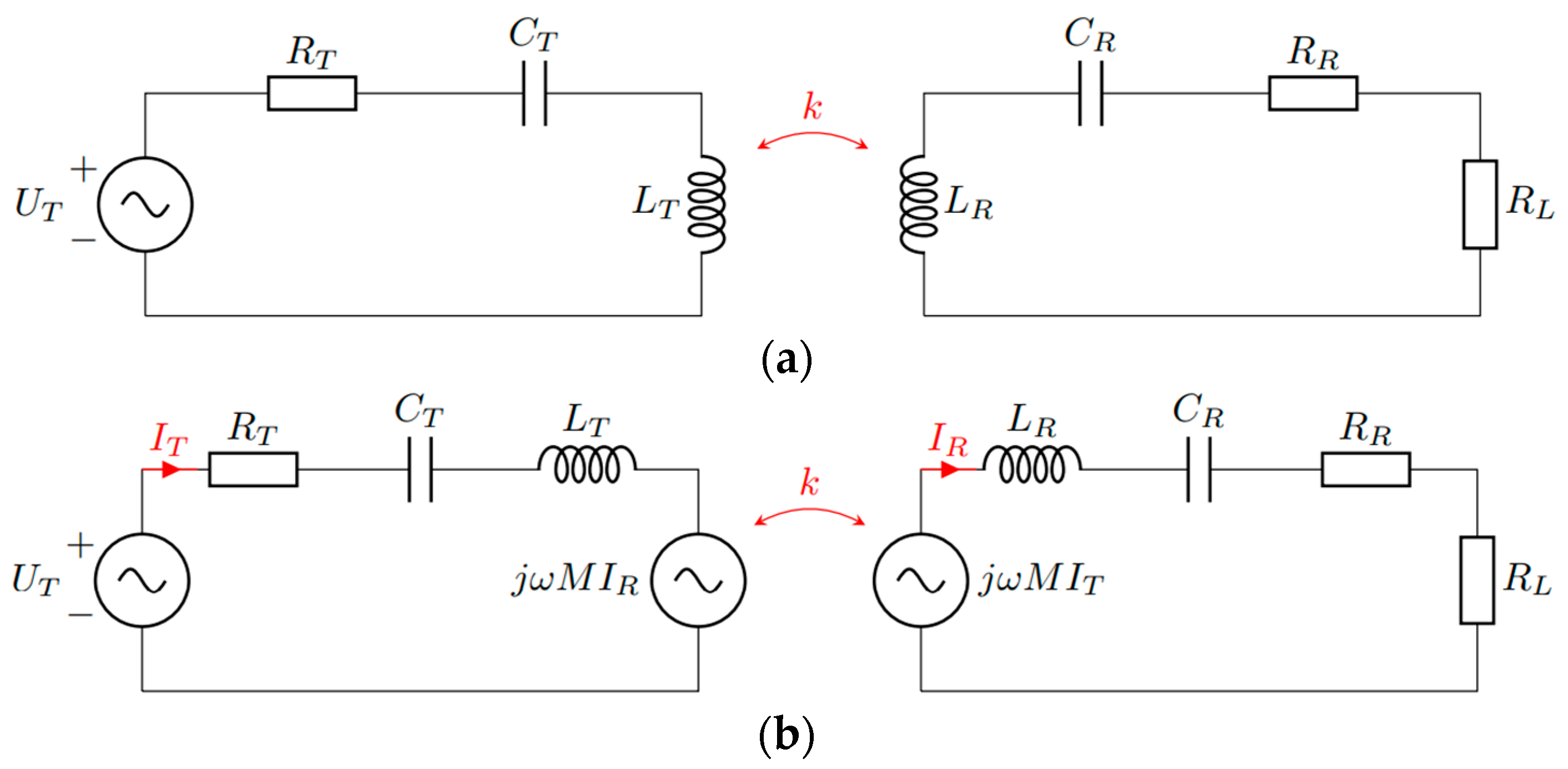
13], proposes that the receiver side is not rotated to the transmitter side. The IPT system transfers power wirelessly via the DD1 transmitter and the receiver coil, which are not coupled with the DD2 transmitter and the receiver coil. Despite the multicoil nature of the system, it can be considered as two separate IPT systems using DD coils. This simplifies the design and the control scheme. A simplified circuit of the single coil system is presented in
Figure 3.
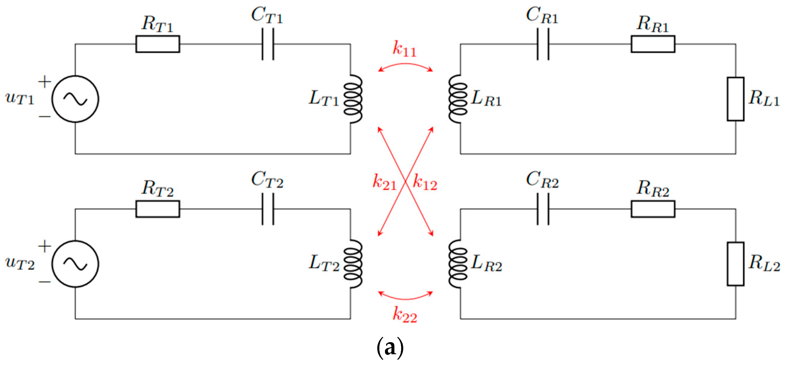
However, the same cannot be considered in the case of rotation between the transmitter and the receiver. When the double DD transmitter and the receiver coil structure are rotated to one another, there is additional cross coupling between the DD1 and DD2 parts of the system.
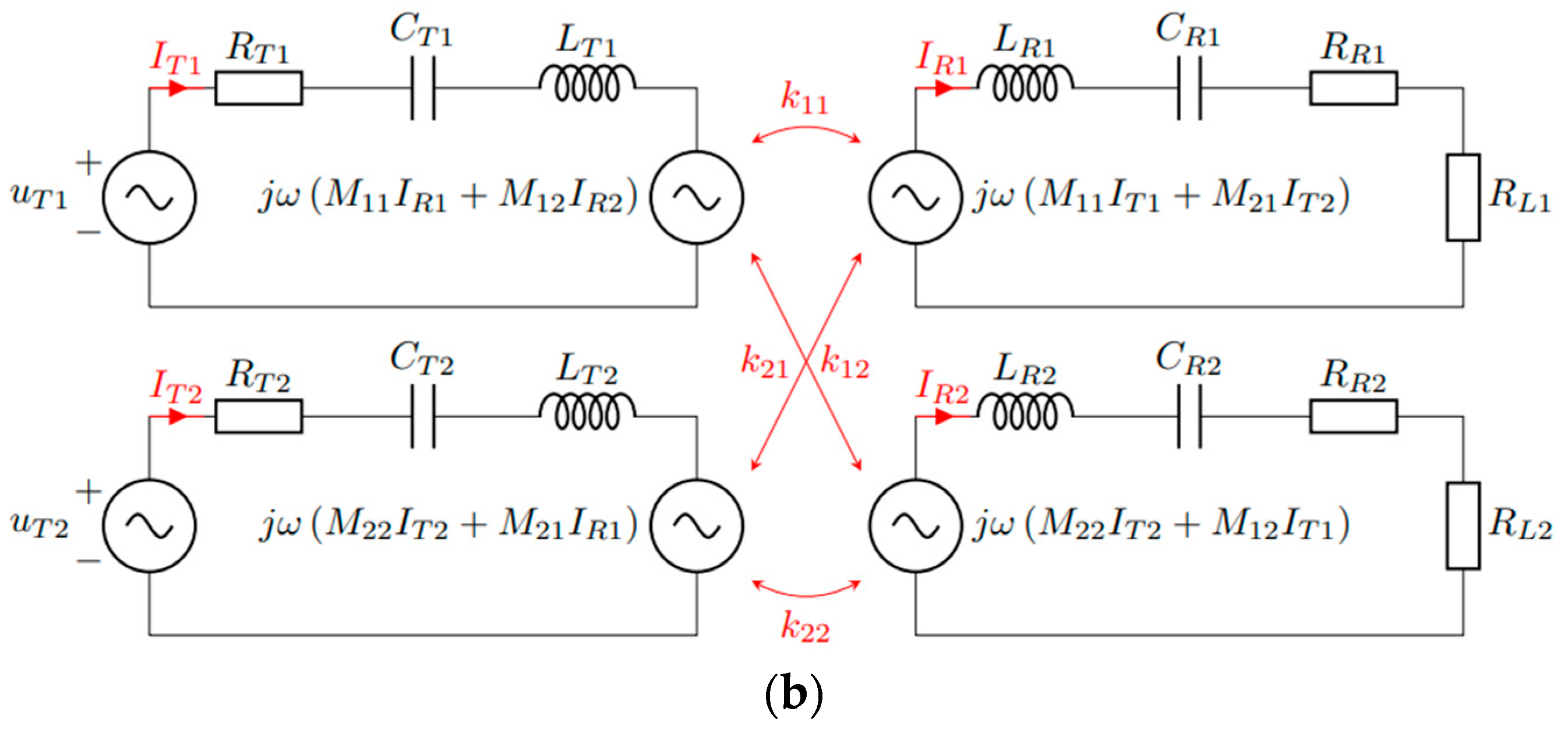
Figure 4 presents a simplified circuit of the system using a double DD coil structure. In addition to the coupling coefficient
k11 between the DD1 coils and
k22 between the DD2 coils, cross coupling between the DD1 transmitter and DD2 receiver coil is marked with
k12, and cross coupling between the DD2 transmitter and DD1 receiver coil with
k21.
Figure 4a presents the simple circuit, and
Figure 4b represent the link between the transmitter and receiver coil with voltage sources representing electromagnetic induction.
When the transmitter coil is rotated to the receiver coil, the coupling coefficient changes. In the case of the DD1 transmitter, k11 decreases and the k12 increases. The same applies to the DD2 transmitter. The coefficient k22 decreases and the coefficient k21 increases. Therefore, the DD1 transmitter coil induces voltage in the receiver DD2 coil, and the DD2 transmitter coil generates voltages in the DD1 and DD2 receiver coils.
3.1. Reduced Circuit Model
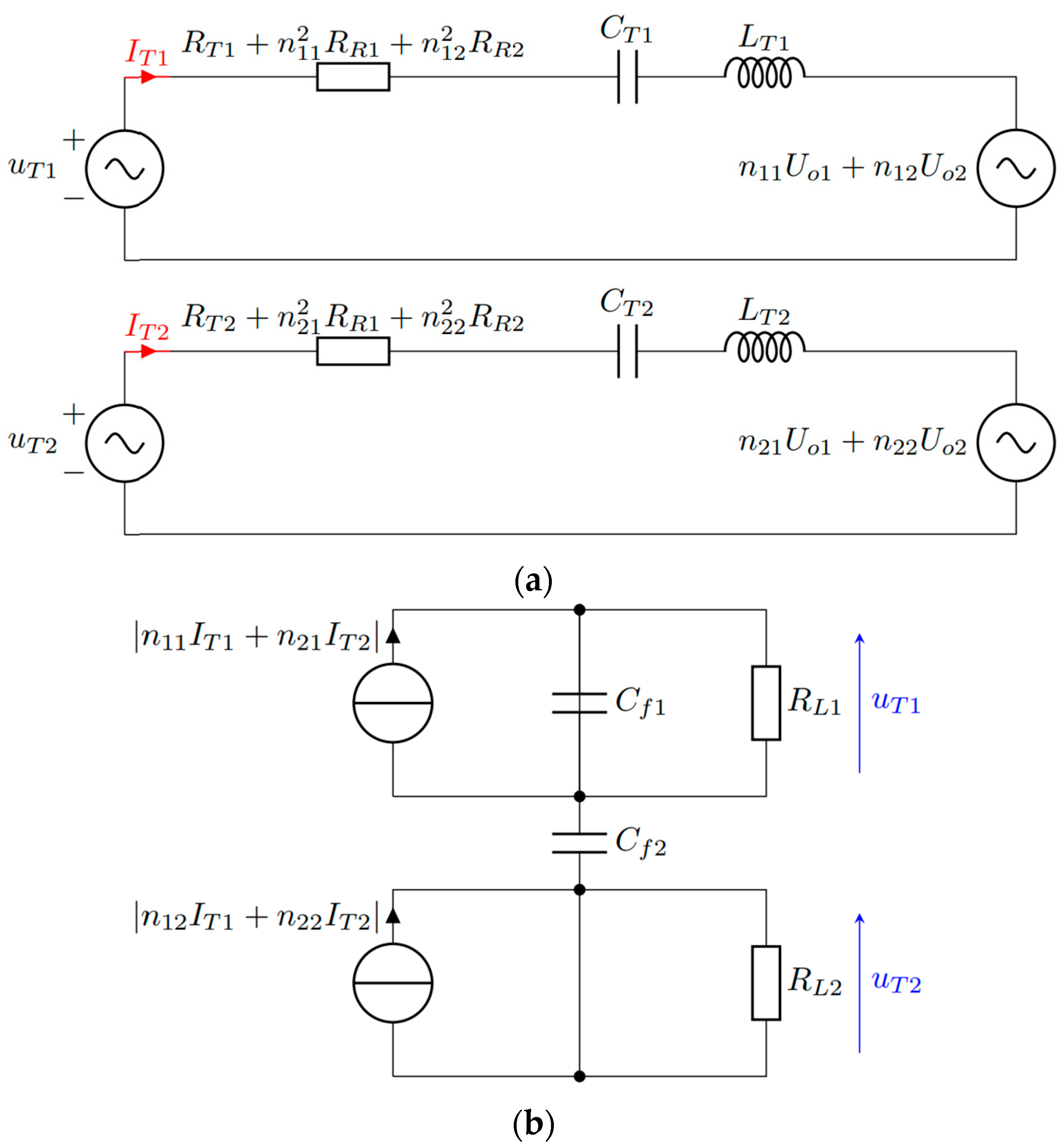
The circuit in
Figure 4 is still complex. The transmitter and the receiver side are still separated, which leads to more complex circuit equations and therefore more complex models. The circuit can be simplified further to a reduced model, similar to the IPT circuit with the basic structure, described in [
15]. The receiving side influences the transmitter side via the gain, marked with
n11,
n12,
n21, and
n22. The gain is dependent on mutual inductance between the coils:
where ω
s is the inverter switching frequency.
RR1 and
RR2 are the resistance of the DD1 and DD2 receivers.
RL1 and
RL2 are loads at the end of the rectifier. In the case of single load,
RL resonator loads are defined as:
The DD1 and DD2 parts of the circuit are excited by the voltage with phase shifted modulation. The first harmonic component of the voltage can be calculated using:
where
uT1 and
uT2 are sinusoidal excitation voltages,
ϕ1 and
ϕ2 are the phase shift of the modulation for DD1 and DD2 parts.
UT1 and
UT2 are the amplitudes of the first harmonic components of the voltage.
The voltage equations, describing the circuit in
Figure 5a take form as:
where
iT1 and
iT2 are the DD1 and DD2 part transmitter currents,
uCT1 and
uCT2 are voltages across the compensation capacitors, and
Uo1 and
Uo2 are the voltages at the end of each of the rectifiers.
The current equations are:
Equations (10) to (13) are describing the resonant parts of the system, which include AC components of currents and voltages. The rectifier circuit, presented in
Figure 5b, includes DC components. The current equations are:
where
Cf1 and
Cf2 are the filter capacitors of the rectifier,
Uo1 and
Uo2 are the voltages at the output of the rectifiers, and
RL1 and
RL2 are the resistive load at the output of the rectifiers.
3.2. Large-Signal Model
The reduced circuit Equations (10) to (15) can be used to derive a non-linear large signal model, which can later be linearized in the operating point using the small-signal model. The main methods for large-signal model derivation are Harmonic Approximation (HA) and approximation using extended describing functions (EDF) [
16]. HA is usually used for sinusoidal waveform, and can be defined as the sum of the sine and cosine signals:
where
x is the periodic signal,
xs is the amplitude of the sine component, and
xc is the amplitude of the cosine component.
Circuit equations also include derivatives. The derivative of HA is:
EDF are usually used for approximation of periodic, non-sinusoidal signals. In the case of a resonant circuit, that applies to both input and output voltages. The input voltages
uT1 and
uT2 are redefined as:
The output voltages
uR1 and
uR2 are defined as:
where
Uo1 and
Uo2 are the output voltages,
iT1s and
iT2s are the sine components of the transmitter currents,
IR1c and
IR2c are the cosine components of the transmitter currents, and
IT1 and
IT2 are the amplitudes of the transmitter currents in steady state in the operating point.
The absolute value of a rectified current can be defined by the equations:
Both methods, HA and EDF, can be used to analyze the circuit equations. The voltage equations therefore take form as:
The current circuit equations take form as:
Equations (24) to (27) include both sine and cosine components. The equations can be simplified by extracting the amplitude of the periodic signals. Equations with sine components are:
The cosine components are:
Finally, the DC components of the circuit are:
The non-linear model consists of 10 Equations (28) to (37).
3.3. Small-Signal Model and Operating Point of an IPT
The operating point of the system must be determined before the linearization. It depends on the coupling coefficient between the coils, the excitation frequency, the phase shift angle of the high frequency inverter, and the resistance of the load. The operating point determines the amplitudes of the currents and voltage in steady state. The operating point of the system is defined by the vector:
where
IT1s and
IT2s are the amplitudes of the sine transmitter current component,
UCT1s and
UCT2s are the amplitudes of the sine capacitor voltage component,
IT1c and
IT2c are the amplitudes of the cosine transmitter current component, and
UCT1c and
UCT2c are the amplitudes of the cosine capacitor voltage component.
The steady state equations of the system are obtained from the large-signal model of the system, and by equating all derivatives with zero. The matrix form of the steady state operating point is defined as:
where
Bst is the steady state input vector and
Ast is the steady state system matrix. If the values of
Ast and
Bst are known, the steady state vector describing the IPT system operating point can be calculated using:
The steady state system matrix and steady state input vector can be calculated using the following matrixes.
Additional variables were used to simplify the equations in matrix form.
Re1 and
Re2 represent the load resistance, mirrored through the full bridge rectifier:
For further simplification, all the resistances of the DD1 and DD2 parts can be added together as:
Finally, the steady state output voltage for each of the rectifiers can be calculated using:
The steady state of the system is used to calculate the small-signal model. The system consists of a steady state and linear small-signal model.
The input vector can be defined as:
The system can be controlled using the phase shifted modulation, change in operating frequency, and with voltage change at the input of the inverter. The IPT structure in our case is more suitably controlled using phase shifted modulation.
The small signal model of the system is defined as:
The input voltage is nonlinear, and must therefore be linearized using Taylor series expansion:
The same must be done for the sine and cosine components of the voltages at the output of the resonant circuit:
Finally, the absolute value of the rectified current can be defined as:
The linearized voltage and current equations can be inserted into the large-signal model of the IPT system. This results in a new set of linear equations, which best describe the dynamics of the system around the operating point. The linear equations can be rearranged into matrix form. The resulting matrices are:
The system matrix A defines the dynamic response of the IPT system. Parameters
Ki are defined with the equations from (63) to (88). Matrix B describes the impact of the input parameters on the inner system states. Vector C is the output vector that defines the connection of the inner states to the output of the system.
4. System Analysis and Control Design
An analysis of the small-signal model of the system must be performed to design the control. The parameters are the same as the parameters of a low-power experimental system. The parameters of the system are presented in
Table 1. Those parameters do not determine the operating point of the system, and do not change on a case by case basis. On the other hand, their value greatly impacts the behavior of the IPT system. The parameters of the system were chosen for a resonant frequency around 85 kHz. Inductors have fixed values based on their geometrical properties. Series compensation capacitors were selected to form a resonant circuit with the specified resonant frequency. In the case of frequency control, the resonant frequency of the circuit would stay the same. Only the frequency of the excitation voltage would change. Control using phase shifted modulation is preferred in the case of full bridge inverters.
The operating point is based on the variables that can be changed. The values used to determine the operating point are presented in
Table 2. The parameters include DC input voltage and operating frequency, which do not change and are constant. The other values, such as the phase shift angle, coupling coefficients, and load resistance, can change during the wireless power transfer.
The operating point of the system can be determined from
Table 2 and the steady state equations. The results for the selected parameters are presented in
Table 3. The steady state values can be used further in calculations for the small-signal model, which can later be used to design the control. Usually, only an integral I or proportional integral PI controller are used in IPT systems [
16,
17,
18]. The integral part eliminates the steady state error, which can happen if the parameters of the model deviate from the parameter of the real system. In the case of this paper, a linear PI controller is used with fixed gain.
The proposed control scheme is presented with the block scheme in
Figure 6. The open loop transfer function G
U(s) of the system is marked with the red square with dotted lines. The system has two inputs and a single output. The inputs are the phase shift modulated voltage of the first and second full bridge high-frequency inverters. The first inverter excites the DD1 transmitter coil, and the second transmitter excites the second DD2 transmitter coil. Each of the coils can be excited separately.
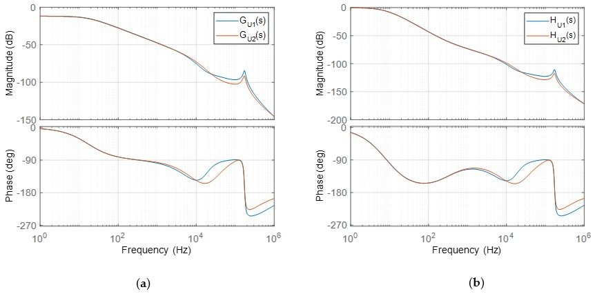
Figure 7a presents the Bode diagram of the open loop voltage transfer function.
Figure 7b presents the Bode diagram of the closed loop voltage transfer function with the PI voltage controller. A controller with the same parameters can be used, because the DD1 and DD2 parts of the system are almost symmetrical. The transfer function of the system controlled with phase shift angle
ϕ1 is marked with blue, and the system controlled with
ϕ2 is marked with red.
The controller was designed with the help of a graphical interface
PIDtool, which is included with Matlab. The controller was designed with fast transient response in mind. The static error is corrected using the integral part. An additional requirement was that the response was without overshoot. The equation of the selected PI controller is:
The next step was to implement the control on the system and check the voltage control under different conditions, such as different voltages, loads, and coupling coefficients.
5. Experimental Results
A small-scale IPT system with the proposed PI control scheme was tested, to test if the IPT system using double DD coils can truly be rotationally independent. The parameters of the system are written in
Table 4. The operating frequency range was selected in the range of Standard SAE J2954 [
19], which proposes an operating frequency around 85 kHz. The resonant circuit was designed for 85 kHz. By selecting the higher switching frequency, in our case 87 kHz, the IPT system operates in the inductive range that enables Zero Voltage Switching [
20,
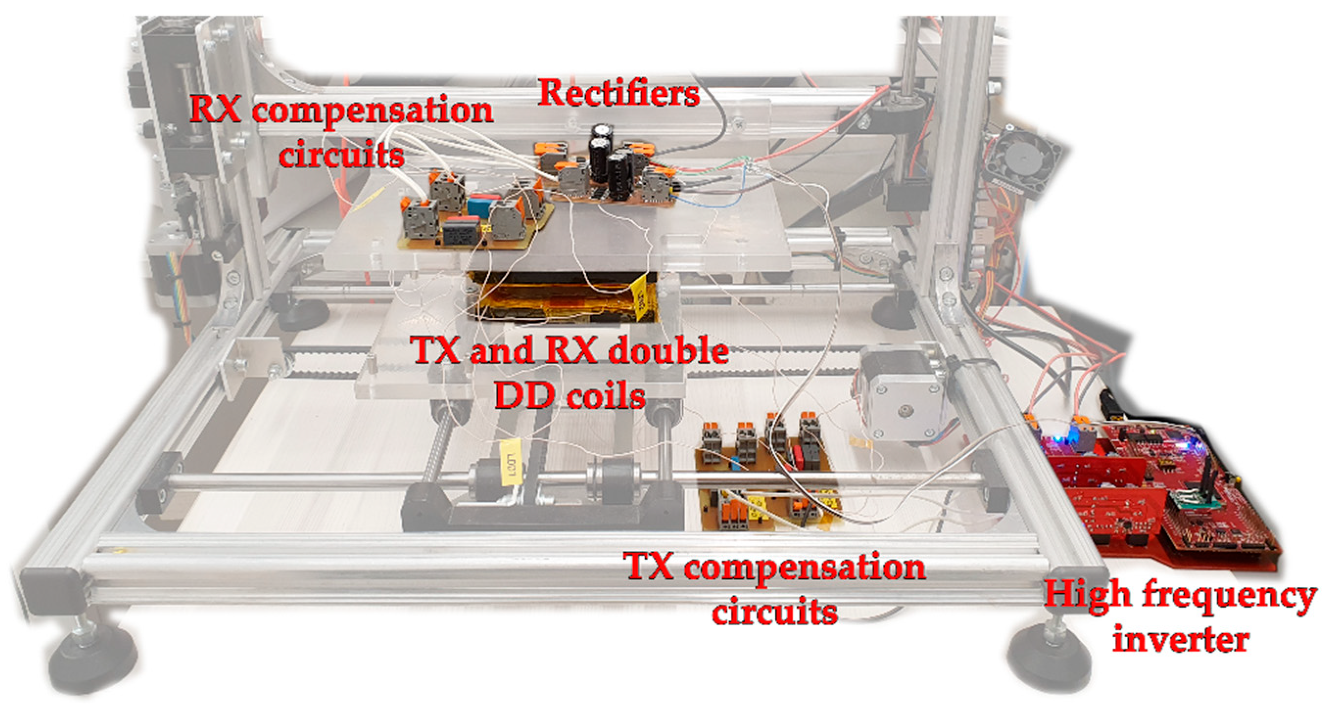
21]. The small-scale experimental system is presented in
Figure 8. The highlighted elements are the main parts of the IPT system using double DD coils. The system consists of a primary, a transmitter side, and a secondary, a receiver side. The transmitter side consists of the high-frequency inverter with two full bridges, each of which drives its own DD coil, compensated by the TX compensation circuits. On the receiving side, the DD1 and DD2 coils are connected to the RX compensation circuits and rectifiers. The rectifiers are further connected to the resistive load. The TX and RX double DD coils were mounted on the 3D positioning mechanism, which enables controlled movement in 3D space.
The PI controller was implemented on a Digital Signal Processor (DSP) that controls the high-frequency inverter. The DSP was also connected to the PC. This enabled the user to change the constant voltage value and to log data from the sensors. This gave the user better control of the experimental IPT system. The main drawback of the interface between the PC and DSP was the communication delay. There was a dead time between the change of the reference value and the change of the output value. The delay was quite significant.
To evaluate the performance of the implemented voltage control, the output voltage must be within certain bounds and under certain conditions. The allowed errors are presented in
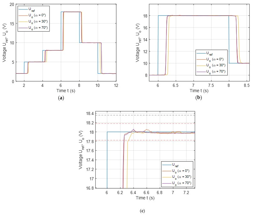
Table 5. The maximum allowed overshoot due to the step voltage reference change, or due to the system parameters change is 2%. The maximum allowed steady-state error, when no additional interference is present is 1%. On the measurement results, the overshoot boundary is marked with a black dashed line, and the steady-state error boundary is marked with a red dashed line.
Figure 9 presents the response of the IPT system when changing the reference voltage. The measurements were performed at three different angles α, at 0°, 30°, and 70°. The voltage reference is marked with a blue line.
Figure 9a presents the multiple step responses.
Figure 9b presents the single step response when the voltage reference was changed from 8 V to 18 V. After 2 s, the reference voltage was changed to 10 V. From the response, it can be seen that the angle α between the coils did not have much impact on the dynamic properties of the system. Only the yellow response, measured at α = 70°, had a small lag behind the other two responses. This was due to the communication delay between the PC and DSP, which was not always constant.
Finally,
Figure 9c presents the voltage overshoot of the PI controller. The maximum error was around 0.05 V, which was less than 0.3% of the output voltage. The PI controller was designed with minimal overshoot in mind. There was also a small steady state error present. The output voltage was lower than the voltage reference value. The difference between the reference voltage and steady state output voltage was, again, less than 0.05 V.
In the case of
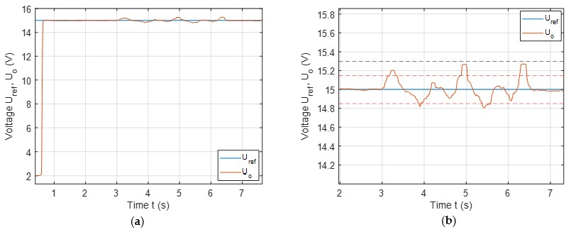
Figure 9, the angle α did not change dynamically during the energy transfer. This is usually the case in all static wireless charging applications. On the other hand, the response of the controlled IPT system when angle α is changing during the transfer is presented in
Figure 10. The reference voltage is marked with the blue color and was set to 15 V.
Figure 10a presents the voltage control on the larger scales, and
Figure 10b presents the voltage control on the smaller scales. On the smaller scale, it can be observed that the absolute maximum error due to the dynamic changing of the α was around 0.25 V, or less than 2% of the output voltage.
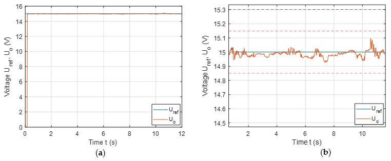
Finally, the influence of the load change on the output voltage is presented in
Figure 10.
Figure 11a presents the load change influence on the output voltage on the larger scale, and
Figure 11b on the smaller scale. The load was changed from 21.4 Ω to 10.7 Ω. The effect of the load change on the output voltage was almost negligible. On the small scale, it can be seen that the biggest difference between the reference value and output voltage was smaller than 0.1 V, or less than 1% of the output voltage.
The load resistance change in IPT systems usually happens due to the change in battery resistance during the charging process. The resistance of the battery depends on the battery state of charge (SOC). However, battery resistance introduces a slow, gradual change in resistance, unlike the step change, presented in
Figure 11.
The results show that the double DD coil structure enables wireless power transfer independent of the angle between the transmitter and the receiver coil, which is a huge upgrade compared to the system using DD coils.
The efficiency of the IPT system is highly dependent on the operating point of the system. This includes the phase-shift angle of the inverters. This means that the efficiency of the proposed IPT system is dependent on the output voltage. The efficiency is smaller at lower voltages and larger at higher output voltages. In the presented results, the highest voltage was 18 V. At that voltage, the efficiency of the system was around 75%. At the output voltage of 5 V, the efficiency was significantly lower—around 52%. Therefore, it is important that the IPT system is designed to operate at higher voltages and larger phase shift angles.
6. Discussion
Unlike classic single DD coil IPT systems, the experimental system using double DD coil structure exhibited tolerance to the rotation. The receiver coil can be rotated to the transmitter coil without a drop in output voltage and significant increase in power consumption. However, rotation angle α does impact on the output voltage. Therefore, the IPT system requires voltage control.
PI voltage control was implemented, based on the linearized small-signal model. The control eliminates a steady state error—the measured voltage is the same as the reference voltage. The robustness of the designed control was tested under different conditions, different coupling coefficients and different loads.
When comparing the step response of the system in different rotations, there was little to no difference. The response was almost the same. The biggest difference in response was when the angle between the transmitter and the receiver coil was changed during the energy transfer. However, the difference was rather small. The error was less than 0.25 V and eliminated quickly.
Additionally, we tested the response of the system when the load was halved. This represented a drastic change, which usually does not happen during the wireless power transfer. The change in load resistance had little to no effect on the output voltage. The steady state error was less than 0.1 V. On the other hand, all changes in the IPT system parameters result in a change in the impedance. The impact of the change in coupling coefficients and the change in the resistive load all impact the reflected secondary impedance on the primary impedance. Both changes result in different output voltage. The coupling coefficient has a greater impact on the IPT system than the change in the load. Additionally, the change in coupling coefficient can be fast compared to the change in load resistance, which usually changes due to the changing resistance of the battery. The battery resistance changes slowly and is dependent on its state of charge (SOC).
The performance of the voltage control was within bounds with the maximum allowed control error, set in
Table 5. The highest voltage overshoot was during the rotation angle α change and still under 2%. The drastic change in the load resistance—a halving of the load, did not impact or create any significant voltage overshoot. The experiment confirmed that an IPT system using a double DD coil structure exhibits rotational tolerance, and can therefore be used as a replacement for classic planar nonpolar coils, which are also not dependent on the rotation between the transmitter and the receiver.
7. Conclusions
This paper presents the control of an IPT system using a double DD coil when the receiver is rotated to the transmitter. The double DD coil is based on the bipolar DD coil. The main advantage of the DD coil is horizontal misalignment tolerance in one of the directions. However, due to the directional magnetic field, the DD coil is not tolerant to the z-axis rotation. When the angle approaches 90°, the coupling coefficient between the transmitter and the receiver coil decreases to zero. Therefore, the DD coil cannot be used for IPT systems where there is a chance of rotation between the transmitter and the receiver.
The double DD coil consists of two perpendicular DD coils. The coils are not coupled and can be excited separately. This leads to higher power density in symmetrical misalignment tolerance. An additional advantage of the double DD coils is also that they have tolerance to the z-axis rotation. However, coil rotation does impact the transferred voltage. Constant output voltage can be achieved using a PI control, designed based on the linear small-signal model. The model was derived from the reduced circuit model of the IPT systems.
The performance of the system was evaluated using a low power experimental setup. Each of the DD coils inside the double DD coil structure were excited by a high-frequency phase shift modulated voltage. The two rectifiers on the receiver side were connected in series and provided power to a single resistive load. In the current configuration, the measured voltage value was transferred to the transmitter side using a wire. This should be replaced by the wireless connection in the future.
The main advantage of the proposed double DD system is that it allows the rotation between the transmitter and receiver coil, unlike the system using single DD coils. Due to the directional nature of the magnetic flux, generated by a single transmitter DD coil, the system is highly dependent on the rotation between the transmitter and the receiver. Double DD coils do solve this problem. The cost is a more complex system model, which can be used to design the output voltage control.
