Article

New Fixed-Frequency Digital Control to Improve the Light-Load Efficiency of an Isolated Regulated Converter

Xi’an Microelectronic Technology Institute, Xi’an 710054, China
*
Author to whom correspondence should be addressed.
Electronics 2023, 12(3), 575; https://doi.org/10.3390/electronics12030575
Submission received: 16 December 2022 / Revised: 7 January 2023 / Accepted: 16 January 2023 / Published: 23 January 2023
(This article belongs to the Topic Power Electronics Converters)

Abstract

:
With the development of environmental and economic requirements, the light-load efficiency of DC/DC converters is increasingly important. However, many isolated regulated converters still use fixed-frequency control, which has low light-load efficiency. This paper proposes a new digital control method to improve the light-load efficiency under fixed-frequency control. On the one hand, new gate-drive timing control is proposed to achieve the soft-switching of the primary switch. On the other, the software voltage–second balance method realizes the synchronous rectification in the discontinuous conduction mode, which reduces the conduction loss. The diagram and workflow of the proposed control scheme are demonstrated at length. A 100-Watt prototype was designed, and the test results show that synchronous rectification and quasi-zero-voltage-switching are realized in the whole operating range at the light load. The light-load efficiency is 81% to 87%, which improves by 5% to 10% in comparison to the traditional forward converter. The prototype also functions well under the load transient. The proposed control scheme is implemented in one digital controller without additional components, and the circuit is low loss and low cost.

1. Introduction

A DC/DC isolated-regulated converter (IRC) converts high bus voltage into low DC voltage, isolates the input and output, and supplies power to electrical equipment. IRCs are widely used in various electronic systems, such as in industry, railways, and satellites. With the application of synchronous rectification, planar transformers, and low-loss components, IRC’s full-load efficiency has been improved by 10–20% in the past twenty years, which ranges from 87% to 95%. However, many power loads only operate for a short time; thus, light-load efficiency is becoming more critical for power converters [1]. For example, many organizations and programs (such as the U.S. Energy Star, Climate Savers, and 80 Plus) [2,3] require high efficiency over a wide load range.
Variable-frequency control (VFC) [4] is an effective method to improve light-load efficiency, which is adopted in computing and fast-charging equipment. However, it has some disadvantages. (1) Many VFC strategies are patent protected, which means that the circuits are difficult to replace. (2) VFC may result in a slower transient response and larger output voltage ripple. (3) EMC (electromagnetic magnetic compatibility) design is difficult over a wide frequency range. Thus, fixed-frequency PWM (pulse width modulation) control is still widely used in high-reliability fields such as aerospace, the military, railways, and in industry, which leads to low light-load efficiency [5].
The mode hopping (MH) technique [6] means that the converter operates in continuous conduction mode (CCM) under medium to heavy load in synchronous mode, while it operates at the discontinuous conduction mode (DCM) under light load in asynchronous mode. In DCM, the inductor current has low ripple and low root-mean-square value, the active switch is zero-current switching (ZCS) turn-on, and reverse recovery loss is eliminated. Thus, the converter has low loss and low noise in DCM.
To further reduce conduction loss, synchronous rectification (SR) in DCM has been researched, where synchronous switches operate in a non-complementary manner [7]. There are mainly three control methods. (1) Detecting the drain–source voltage of the freewheeling switch. The switch is disabled when its voltage drops below the threshold voltage [8]. The threshold voltage requires high precision. (2) Detecting the zero current of the inductor current by a ZCD (zero-cross detector) circuit and turning off the freewheeling switch [9,10,11]. (3) Using the voltage–second balance method [6,12,13]. The freewheeling switch turns off when the inductor current returns to the initial value. However, the above techniques are realized by analog circuits and specific controllers, which are expensive, and difficult to replace, and it is hard to obtain hi-rel products.
Although the active switch is naturally ZCS turn-on under DCM, its parasitic capacitive loss still exists. Thus, ZVS (zero voltage switching) turn-on under DCM has been studied for decades. In the flyback circuit [14,15], a coupled inductor is in series with a resonant capacitor and an auxiliary switch. When the auxiliary switch turns on, the resonant capacitor produces a reverse inductor current. The reverse current discharges the parasitic capacitor, and the primary switch turns on under ZVS. In [16], the ZVS turn-on is realized by turning on the active clamp switch for a short time. In the synchronous buck circuit [17,18,19,20], two auxiliary switches are parallel with the inductor. The reverse inductor current is retained when the auxiliary switches turn on, and the active switch is ZVS turn-on. However, the continuous reverse current causes extra conduction loss. The systems in the above papers need additional power components and gate-drive circuits, increasing the cost and circuit area.
In this paper, a new fixed-frequency digital control scheme is implemented to improve the light-load efficiency of IRC. The proposed software voltage–second balance method realizes the synchronous rectification in DCM and reduces the conduction loss. The quasi-ZVS turn-on of the primary switch is realized by new gate-drive timing. In addition, the control mode is digital peak current mode (DPCM). The control scheme is implemented in a digital MCU (micro-controller unit), with low cost and low loss. The circuit has no additional power components and specific integrated circuits (ICs).
Section 2 analyzes the working principle of the synchronous forward converter in DCM, then introduces the voltage–second balance method and operation modes. The control block diagram and its workflow are demonstrated in Section 3, with key parameters designed. Section 4 gives the specifications and parameter selection of the 100-Watt prototype. Section 5 shows the test waveforms and results and compares them with other papers. Finally, Section 6 concludes the work.

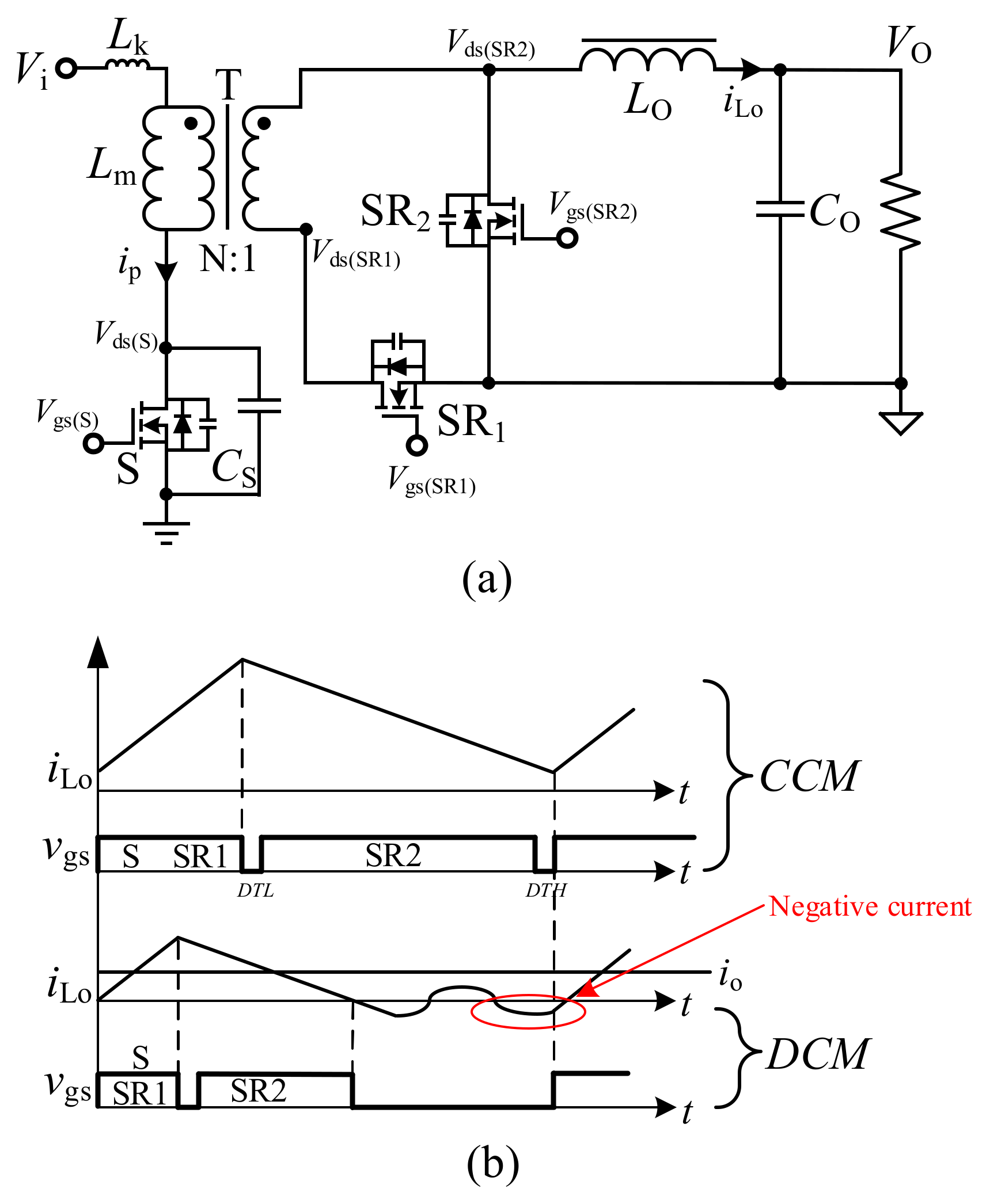
2. Working Principles in DCM

2.1. Soft-Switching of the Primary Switch

The forward converter with synchronous rectification is shown in Figure 1a. The magnetizing inductor of the transformer is reset and is resonant with the equivalent resonant capacitor CS. The gate-drive signals of metal-oxide-semiconductor field-effect transistors (MOSFETs) come from the control circuit. Figure 1b shows that the converter works in CCM at medium and heavy loads. The synchronous rectifiers, SR1 and SR2, conduct complementarily; thus, the output current iLo forms a triangular waveform above zero.
In contrast, the converter operates in DCM at light load. SR2 turns off when iLo drops to zero, then CS reflects to the secondary side and resonates with LO. The resonant current oscillates around zero. If SR1 turns on when iLo goes negative, the resonant current reflects to the primary side, and CS discharges quickly. Thus, the primary switch’s voltage drops, preparing for the ZVS turn-on. The resonant frequency’s expression is shown in Equation (1), where N is the turns ratio of the transformer and Cr is the parasitic capacitance of the secondary side.
f r = 1 2 π ( C S N 2 + C r ) L O

2.2. The Voltage–Second Balance Method

As mentioned above, SR2 turns off exactly when iLo drops to zero. The voltage-second (volt-sec) balance method can generate the gate-drive signal of SR2. In the steady state, the inductor obeys the volt-sec balance principle. That is, the inductor’s magnetization and demagnetization energy are equal in one cycle. For the output inductor LO in Figure 1a, the volt-sec balance is expressed as:
( V ds ( SR 2 ) V O ) t mag V O t dmg = 0
where the dead time is ignored. In Equation (2), tmag is the magnetizing time, and tmag = DTs, where D is the duty cycle and Tsw is the switching period. tdmg is the demagnetizing time, which equals the on-time of the freewheeling switch SR2. Vds(SR2) = Vi/N, which means the input voltage reflects to the secondary side. Substituting the above parameters into Equation (2), we obtain tdmg in Equation (3).
t dmg = ( V i N V O 1 ) D T sw
We derive from Equation (3) that tdmg = (1 − D)Tsw in CCM. Thus, SR1 and SR2 turn on in a complementary manner. While in DCM, SR2 turns off when the demagnetization completes, and the inductor current decreases to zero. Thus, the voltage–second balance principle holds both in CCM and DCM.
As stated in the introduction, the analog circuit implementation of the volt-sec balance method has disadvantages. Thus, a software volt-sec balance method is proposed in this paper. From Equations (2) and (3), we can calculate the turn-off time of SR2, tSR2off.
t SR 2 off t mag + t dmg V ds ( SR 2 ) D T sw V O
If we sample VO, Vds(SR2), and duty cycle D, tSR2off is calculated by the program. The software implementation method is more flexible and does not require additional hardware components.

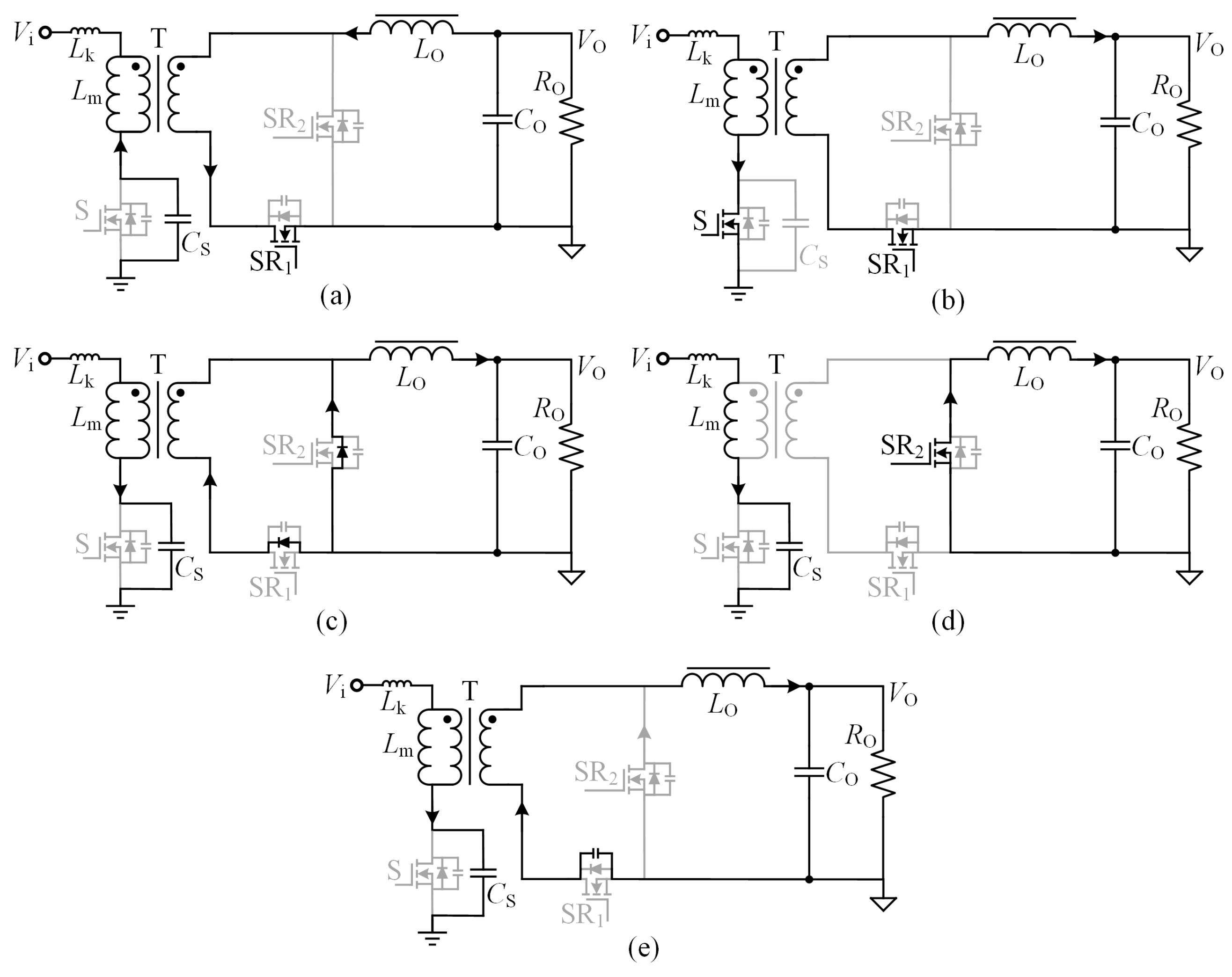
2.3. Operation Modes

The operating cycle is divided into five modes, the key waveforms are shown in Figure 2, and the equivalent circuits of each mode are shown in Figure 3.
Mode 1 (t0t1): SR1 turns on at t0, and the reverse current reflects to the primary side. Magnetizing inductor Lm resonates with reset capacitor CS, and CS is discharged. The drain–source voltage of S (Vds(S)) drops to a minimum value, providing quasi-ZVS conditions for S. The duration of this mode is tZVS, which is set by the software.
Mode 2 (t1t2): S turns on under quasi-ZVS at t1. Inductance Lm and LO are both magnetizing, which causes the current to rise linearly and reach its peak at t2. The expressions are shown in Equations (5) and (6). On the secondary side, SR1 continues conducting, and SR2 is off. The duration of this mode DTS, which is the on-time of S.
I p ( t ) = V i L m + L k t
I L o ( t ) = V i N V O L O t
Mode 3 (t2t3): S and SR1 turn off at t2, and the secondary-side current flows through the body diode of SR1. When Vds(S) rises to input voltage Vi, a voltage spike occurs by the leakage inductance Lk, and SR switches start to commutate. The duration of this mode is the dead time DTL, which is very short. Thus, the inductor current is considered constant. Vds(S) expression is shown in Equation (7).
V ds ( S ) ( t ) = V i + L k C S I p ( t 2 )
Mode 4 (t3t4): When the SR commutation completes, SR2 turns on under ZVS. Lm resonates with CS. LO demagnetizes, and the current ILo decrease linearly. ILo decrease to zero at t4, and SR2 turns off by the voltage–second balance logic in MCU. The duration of this mode is shown in Equation (3). The expressions of Vds(S), Ip, and ILo are shown in Equations (8) and (9).
V ds ( S ) ( t ) = V i + V cp sin ( ω 1 t ) I p ( t ) = C S ω 1 V cp cos ( ω 1 t ) I Lo ( t ) = I Lo ( t 3 ) V O L O t ω 1 = 1 C S L m
where
V cp = L m C S I Lm ( max ) 2
Mode 5 (t4t0): All of the power switches are off at t4, and the output energy is maintained by the output capacitor CO. CS reflects to the secondary side and resonates with LO. The Vds(S) and ILo expressions of this stage are shown in Equation (10).
V ds ( S ) ( t ) = V i sin ( ω 2 t + π 2 ) I Lo ( t ) = N C S V i ω 2 cos ( ω 2 t + π 2 ) ω 2 = 1 N C S L O

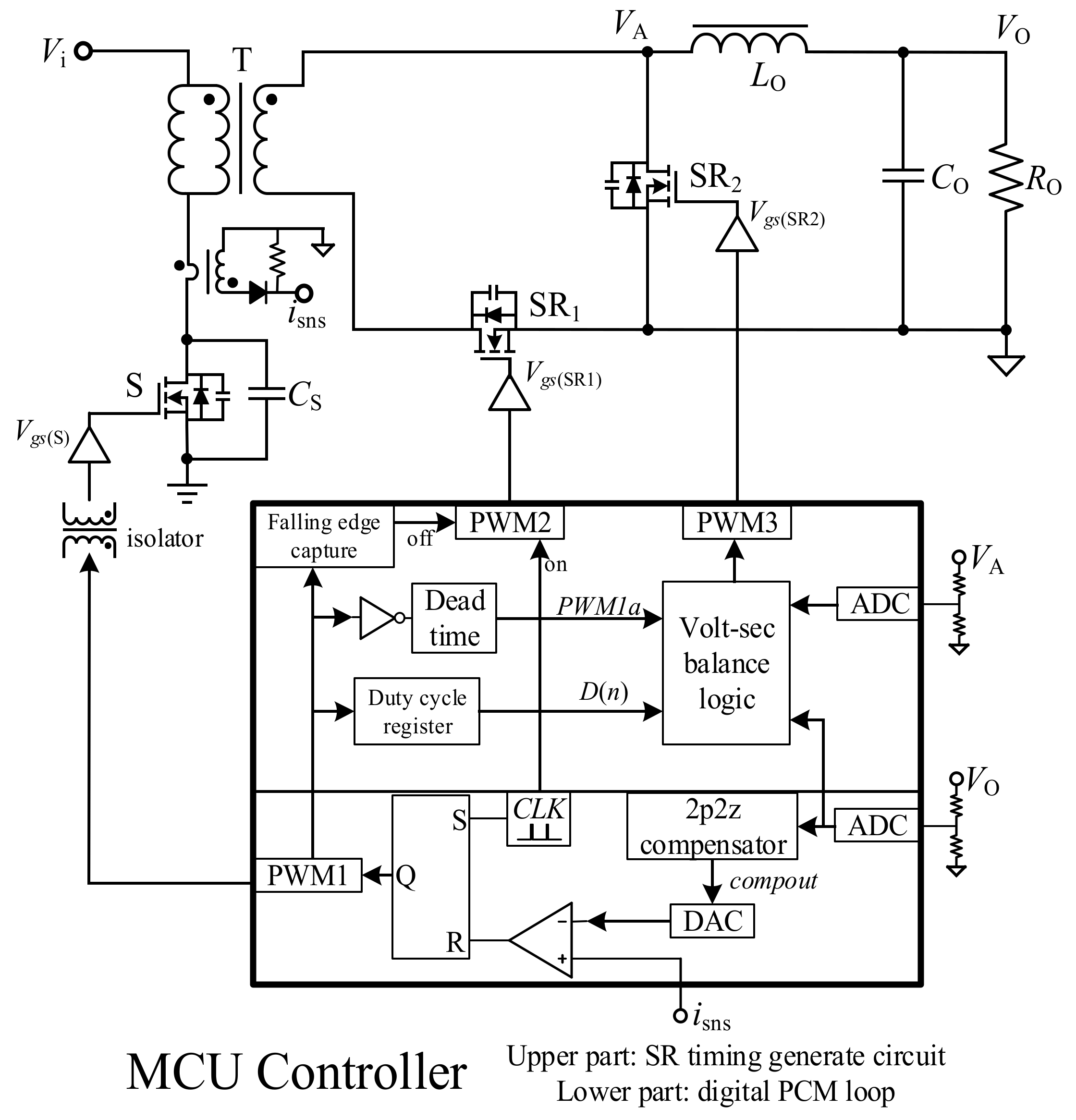
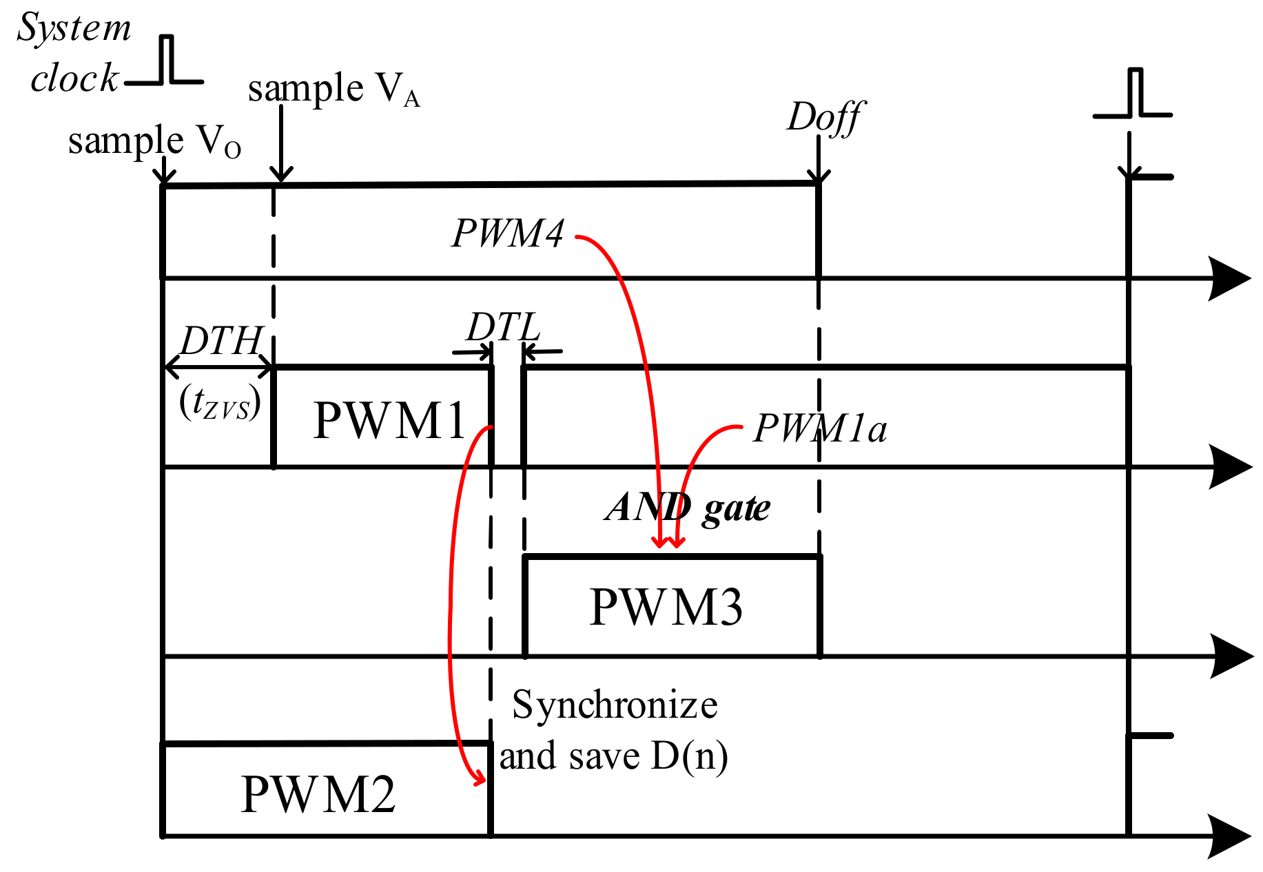
3. The Proposed Control Scheme

3.1. Control Diagram in DCM

The functional block diagram of the proposed control scheme is shown in Figure 4, which works in DCM and in steady state. The power stage is an SR forward circuit with the resonant capacitor reset. Because SR is realized under full load, there is no need for parallel Schottky diodes. The control mode is digital peak-current-mode (DPCM), which consists of an MCU, a signal isolator, and three gate drivers. The MCU controller’s upper part is the SR timing generate circuit, and the lower part is the DPCM control loop.
The DPCM control loop generates the switching signal of PWM1. After the DTH delay of the system clock pulse, the PWM1 turn-on signal is generated. Then, the controller samples the output voltage and calculates the 2p2z compensator program. The output signal compout is converted by DAC and is compared with sampled primary current isns. Finally, the turn-off signal of PWM1 is generated.
In DCM, PWM2, PWM3, and PWM4 are enabled. The PWM2 turn-on signal synchronizes with the clock pulse, and its turn-off signal synchronizes with the PWM1 turn-off signal. The complementary signal of PWM1 is generated, and its duty cycle D(n) is updated. PWM1a, D(n), and VA are processed by volt-sec balance logic and generate the PWM3 signal. The detailed workflow will be demonstrated in the next subsection.

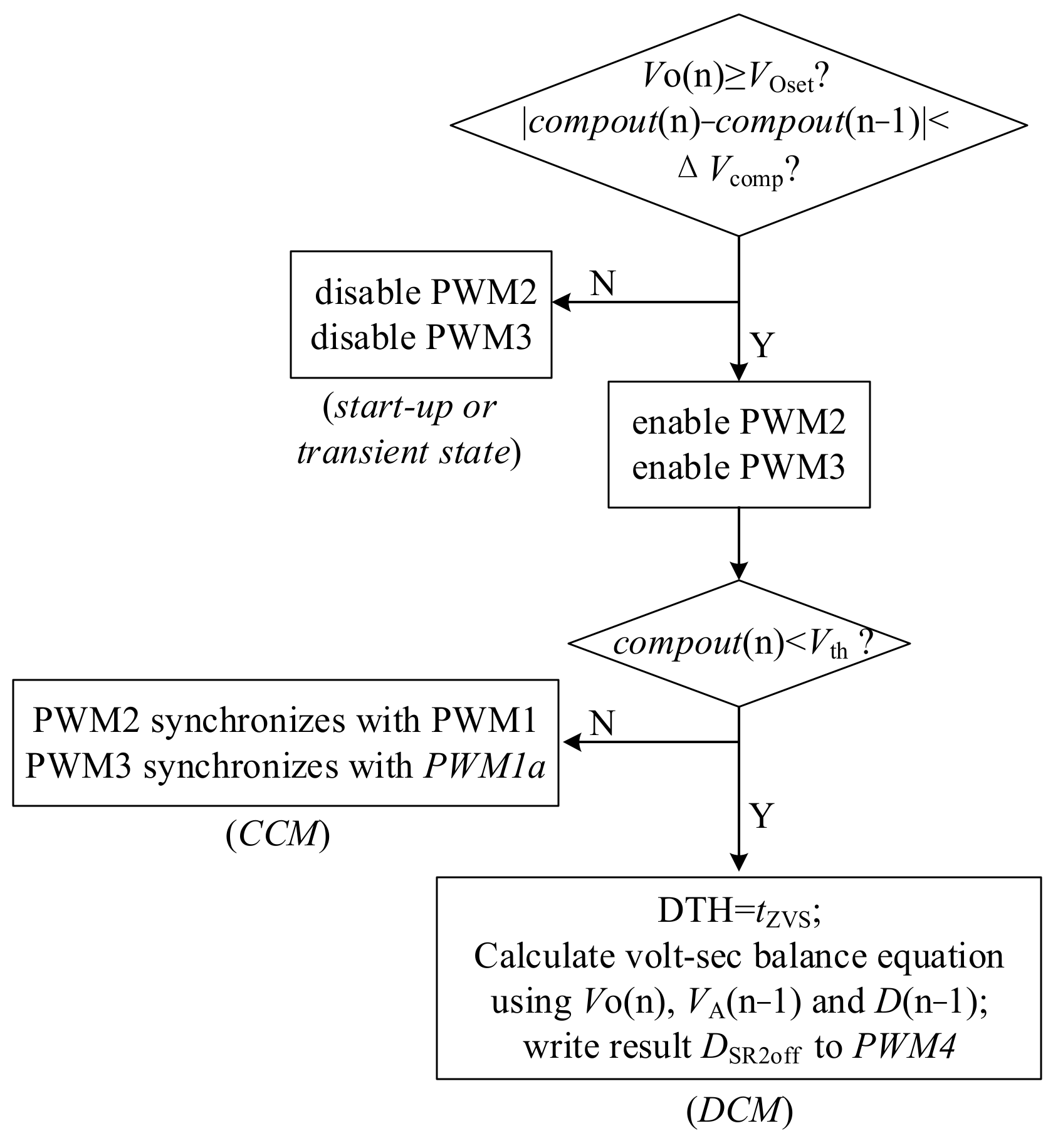
3.2. The Principle of Control Flow

The control flow chart in DCM is shown in Figure 5. The program code is on the left, mainly for loop compensation, working mode judgement, and voltage–second balance calculation. The initialize program enables PWM1 and sets dead time values. Then, the system clock pulse triggers the analog to digital converter (ADC) sample and enters the interrupt program. In the interrupt, a two-poles-two-zeros (2p2z) compensator is calculated, and the result is stored in compout. Then, the working state of the circuit is judged, and the corresponding configuration is performed. Here, it works in DCM. The program ends after exiting the interrupt program.
The right part is the circuit flow in MCU. The clock pulse also triggers the PWM2 rising edge and updates the duty cycle; PWM1 goes high after the DTH delay. When quitting the interrupt program, the circuit executes slope compensation and PWM comparison, finally generating the turn-off signal of PWM1. The falling edge of PWM2 is synchronized with PWM1, and outputs to PWM2 input/output (I/O) port. Then, PWM1 generates a complementary signal PWM1a after DTL delay. PWM4 is obtained by voltage–second balance, passes through AND gate with PWM1a, and outputs to the PWM2 I/O port.
The program flow of circuit state judgement and configuration is shown in Figure 6. If the output voltage is lower than the nominal value (VOset), or the variation of compout signal over a threshold (ΔVcomp), the circuit is considered to operate in a transient state; otherwise, it operates in a steady state. In the transient state, PWM2 and PWM3 are disabled. Thus, SR switches are turned off. If the circuit works in a steady state, further judgement is made by comparing the compout signal with the other threshold (Vth). The circuit works in CCM if compout > Vth. PWM2 synchronizes with PWM1 and PWM3 synchronizes with PWM1a. On the other, the circuit works in DCM if compout < Vth.
In DCM, the program assigns tZVS to DTH, performs the volt-sec balance calculation, and finally obtains the turn-off timing of SR2, whose value is stored in variable DSR2off. The expression of DSR2off is:
D SR 2 off ( n ) = V A ( n 1 ) D ( n 1 ) V O ( n )
Then, the program assigns DSR2off(n) to the duty cycle register of PWM4. Finally, the hardware circuit performs the AND logic of PWM1a and PWM4, which generates the PWM3 signal. The timing sequence and relationship of PWM signals are drawn in Figure 7.

3.3. Design Considerations

3.3.1. Dead Time in DCM

In operation Mode 1 (t0t1), the initial values of the drain–source voltage of S, Vds((t0), and the primary-side current Ip(t0) are related to the load current and dead-time. The dead-time DTH value is tZVS in DCM, which should be carefully designed to realize soft switching. If tZVS is too large, the positive current at the secondary side will reflect to the primary side, and Vds(S) will increase. If tZVS is too small, the negative current energy transferred to the primary side will be small, and ZVS will not be realized. tZVS should not exceed half of the resonant period in Mode 5, whose expression is Equation (1). Here, we set tZVS as 2/3 of the half resonant period; see Equation (12).
t ZVS = 2 π 3 ( C S N 2 + C r   L O
According to energy conservation law, the relationship between Vds(S) and Ip in Mode 1 is:
1 2 C S V ds ( t 0 ) 2 1 2 C S V ds ( t 1 ) 2 = 1 2 L m I Lm ( t 0 ) 2 1 2 L m I L m ( t 1 ) 2
V ds ( t 1 ) = V ds ( t 0 ) 2 L m C S I Lm ( t 0 ) 2 + L m C S I Lm ( t 1 ) 2
where
I L m ( t 1 ) 0 I L m ( t 0 ) = N V i n C S + N 2 C r L O
The Vds(t1) value should be as low as possible to realize the ZVS turn-on.

3.3.2. The Voltage Threshold of the Compout Signal

In DPCM control, the PWM waveform is generated by comparing compout and isns. Thus, compout is proportional to the peak primary current Ipp and the load current IO. This way, compout can judge whether the circuit is working in CCM or DCM. The relationship between compout and Ipp is:
V c o m p o u t = I pp R S N S
NS is the turns ratio of the current sample transformer, and RS is the sampling resistor. In forward topology, the relationship between Ipp and IO is:
I pp = I O N + Δ i pp Δ i pp = D T sw 2 [ V i L m + V i N V O L O ]
The expression of CCM/DCM boundary load current IOB is:
I OB = ( V i N V O ) D T sw 2 L O
Consider Equations (16) and (17) simultaneously. When the load current equals IOB, the compout threshold voltage Vth is obtained, whose expression is:
V th = R S D min T sw 2 N S [ V i ( max ) L m + V i ( max ) N V O L O N + 1 N ]

3.3.3. The Voltage Threshold of the Compout Variation Rate

In the start-up or transient state, the load current changes quickly, and so it is the compout signal. Comparing the difference between the compout value with the previous cycle, when it is greater than ΔVcomp, the circuit operates in a transient state. Suppose the transient load current slope is xA/μs. We assume ΔVcomp is 50% of the transient load slope. The ΔVcomp expression is:
Δ V comp = 0.5 x T sw R S N N S

3.3.4. Controller Selection and Comparison

The program occupies 6.7 kB of the MCU memory, and the data occupy 1.03 kB. We used 16-bit MCU dsPIC33CK32MP502. Its memory size is 32 kB, central processing unit (CPU) frequency is 100 MHz, and it has four PWM outputs. We compared dsPIC33CK32MP502 with other forward SR controllers in Table 1. This controller has a comparable price with old controllers and is much cheaper than the latest controllers.

4. Circuit Design

To verify the above theories, we designed an SR forward converter with DPCM, whose key parameters are shown in Table 2. The 28 V bus voltage is widely used in the military, in satellites, and in industrial applications, while 15 V is the input voltage of various loads, such as airborne computers, industrial computers, and cameras.

4.1. Hardware Parameters

Based on Equation (18), the CCM/DCM boundary current IOB at the minimum input voltage (20 V) is 0.8 A; at the typical input (28 V), it is 1 A; at the maximum input (36 V), it is 1.15 A.
Vds(S) should drop to Vi to reset the transformer before the next period. Thus, half of the resonant reset period should be smaller than the minimum reset time, which is expressed in (21).
π C S L m < ( 1 D max ) T s w
By substituting known parameters into (23), we obtain Cs < 3nF. From Equation (14), Vds(t1) should be as small as possible, and CS should be large to realize soft switching. Here, we set CS = 2.2 nF.
The primary switch’s maximum voltage may occur at the turn-off spikes or the resonant reset peak. Spike voltage can be calculated by Equation (7). At max input and full load, we derive that the max peak primary current is 12 A, and the max voltage spike is 116 V. Equations (8) and (9) show that the max peak reset voltage is 60 V at maximum input. Therefore, the switch stress is 12 A/116 V. Based on a 70% derating design, we choose a 30 A/150 V MOSFET as the primary switch. Ten A/One hundred V MOSFETs were chosen as synchronous rectifiers.
It is worth noting that the prototype is oriented to high-reliability applications such as ground systems, railways, and avionics. Thus, high-reliability components are selected, that is, components that have been screened for reliability.

4.2. Software Parameters

By substituting parameters and calculating Equation (12), we obtain tZVS ≈ 420 ns, where Cr ≈ 2 nF. Here, we set tZVS = 400 ns. Substituting Vds(t0) = 28 V into Equation (14), we obtain Vds(t1) ≈ 5 V. Thus, quasi-ZVS turn-on is realized.
DTL is the dead time between the falling edge of S and the rising edge of SR2. DTL should be as small as possible to minimize the body diode conducting time. In the worst case, the maximum turn-off time of S is about 30 ns, the maximum turn-on time of SR2 is about 20 ns, and the typical delay of the isolator and gate driver is 20 ns. Here, we set DTL equal to 100 ns.
The slope of the transient response is x = 0.6 A/μs. Substituting known parameters into Equations (19) and (20), we calculate Vth ≈ 0.502 V and ΔVcomp ≈ 0.314 V, where VOset = 15 V.

4.3. Power Loss, Ripple, and Regulation Estimation

With the synchronous rectification and quasi-ZVS turn-on under DCM, the prototype has low conduction loss and low switching loss. However, the traditional forward circuit still uses hard-switching and Schottky rectification. The estimated light-load power loss comparison between the proposed and the traditional circuit is shown in Figure 8, under 0.5 A load and 28 V input. The hard-switching loss is high; the primary switch loss is reduced by 82% when soft switching is realized. The secondary conduction loss reduces with SR, but the gate-drive loss is introduced; thus, the rectifier switch loss is reduced by 20%. The control board loss slightly increases because of the additional gate-drive signals. To sum up, the light-load efficiency increased by 10% using the proposed control scheme.
The output voltage ripple estimation is shown in Equation (22), where the ESR of output capacitors is 10 mΩ, and the calculated ripple voltage is 30 mV.
Δ V O = ( E S R + 1 8 C O f s ) V O ( 1 N V O V i ) L O f s
The output voltage regulation estimation is shown in Equation (23), the input disturbance is the second item, and the load disturbance is the third item, where T(s) is the loop gain, Gvg(s) is the audio sensitivity, and ZO(s) is the output impedance. In forward topology, the DC gain of Gvg(s) is the duty cycle D, and the DC gain of ZO(s) is the load RL. Assuming that the DC loop gain is 40 dB, it can be estimated that the input regulation is 28 mV and the load regulation is 47 mV.
V O ( s ) = V ref ( s ) k T ( s ) 1 + T ( s ) + V i ( s ) G vg ( s ) 1 + T ( s ) i O ( s ) Z O ( s ) 1 + T ( s )

5. Experimental Results

The prototype is fabricated based on the above parameters, and its picture is shown in Figure 9. The circuit board consists of a power board and a control board. The USB (universal serial bus) port of the PC powers the control board. The program downloader downloads the program to MCU from the PC. The control board samples the input signals from the power board, processes input signals by MCU, and then outputs gate-drive signals to the MOSFET drivers on the power board. The connection wire length between the control board and the power board has been minimized. It was found that the connection wire delay is less than 10 ns, which can be ignored.

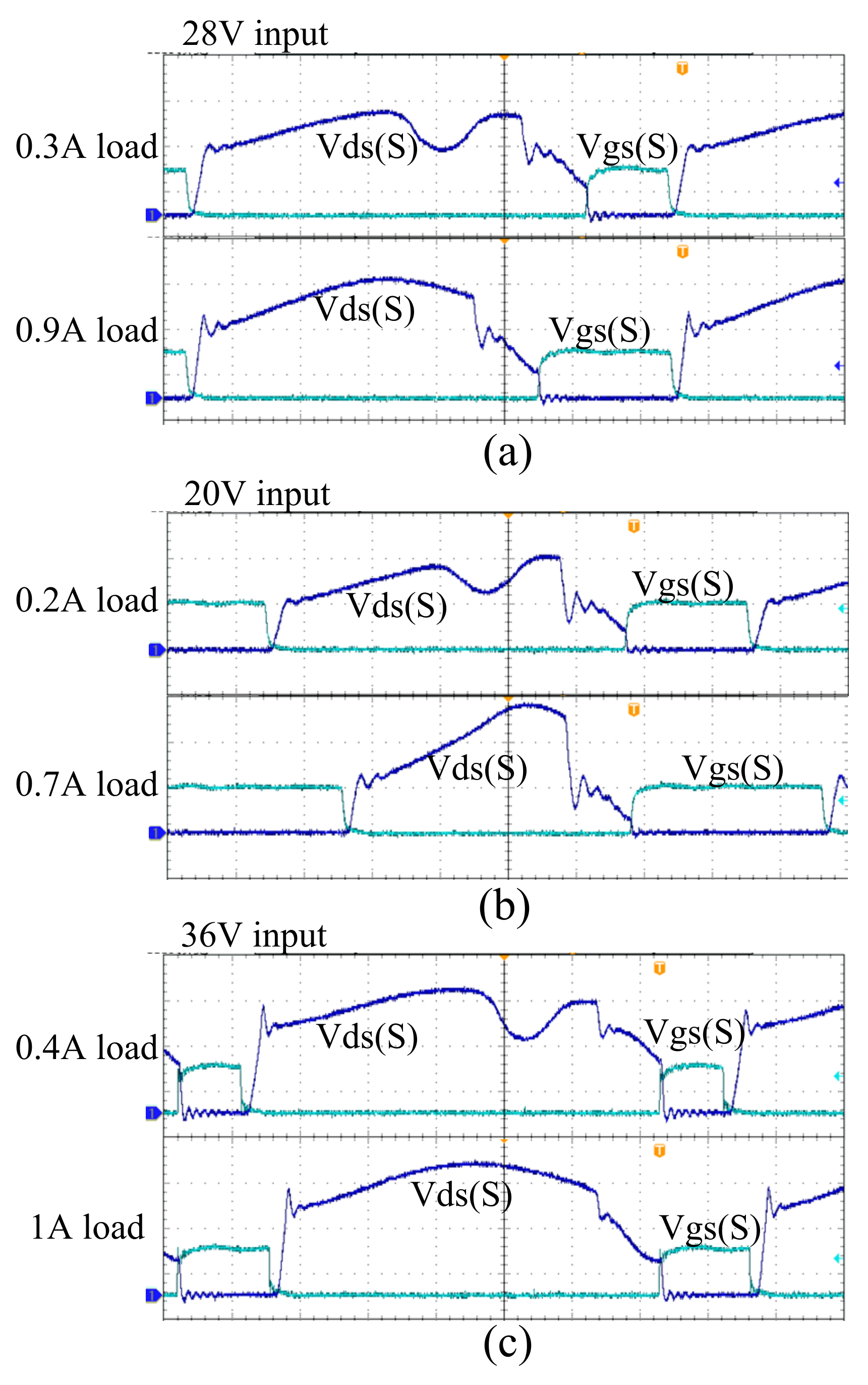
5.1. Waveforms in DCM

Figure 10 shows the gate-drive signal and inductor current waveforms under different input voltages and different loads in DCM. The waveforms in each figure are Vgs(SR1) and Vgs(S), Vgs(SR2), and ILo, from top to bottom. From each figure, SR1 always turns on 400 ns earlier than S, which is tZVS. With the proposed software voltage–second balance method, SR2 turns off exactly when ILo drops close to zero. Therefore, synchronous rectification in DCM is achieved.
Figure 11 shows the drain–source voltage Vds(S) and gate-drive voltage Vgs(S) of the primary switch S under different input voltages and loads in DCM. After S turns off, Vds(S) rises to its peak. The maximum Vds(S) is 60 V at 36 V input, which is consistent with the calculated value. After SR1 turns on, Vds(S) decreases in resonance, and S turns on when Vds(S) drops to the minimum value. (1) At 28 V input, which is shown in Figure 10a, Vds(S) resonances from 44 V to 10 V at 0.3 A load; it resonances from 46 V to 8 V at 0.9 A load. The minimum voltage is basically consistent with the calculated value (5 V). (2) At 20 V input, which is shown in Figure 10b, Vds(S) resonances from 40 V to 8 V at 0.2 A load; from 52 V to 6 V at 0.7 A load. (3) At 36 V input, which is shown in Figure 10c, Vds(S) resonances from 46 V to 20 V at 0.4 A load; it resonances from 46 V to 14 V at 1 A load. Thus, S turns on under quasi-ZVS is realized in DCM.

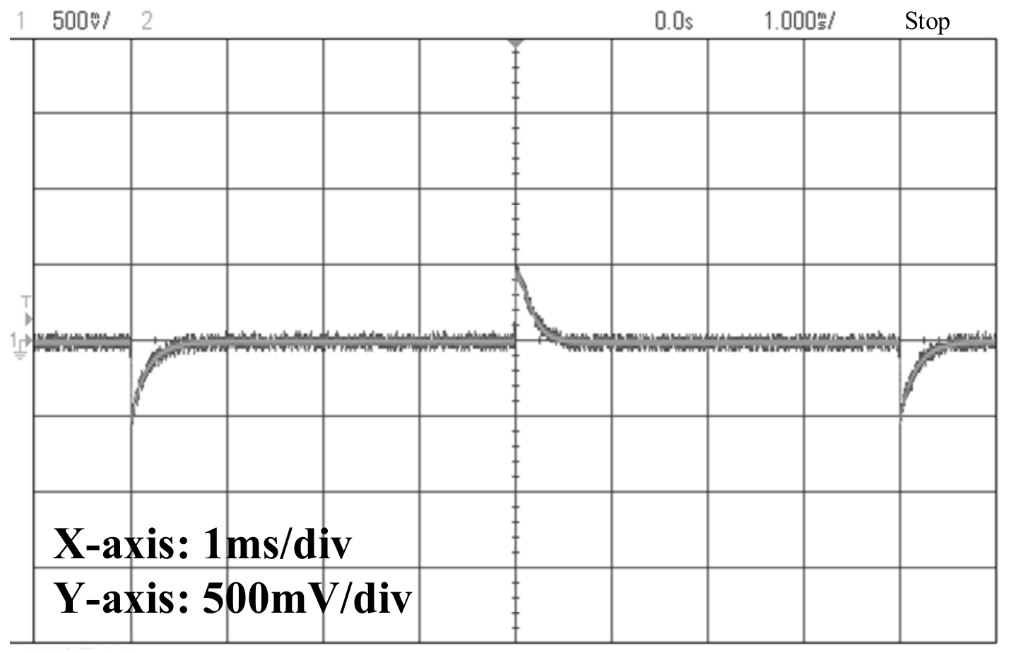
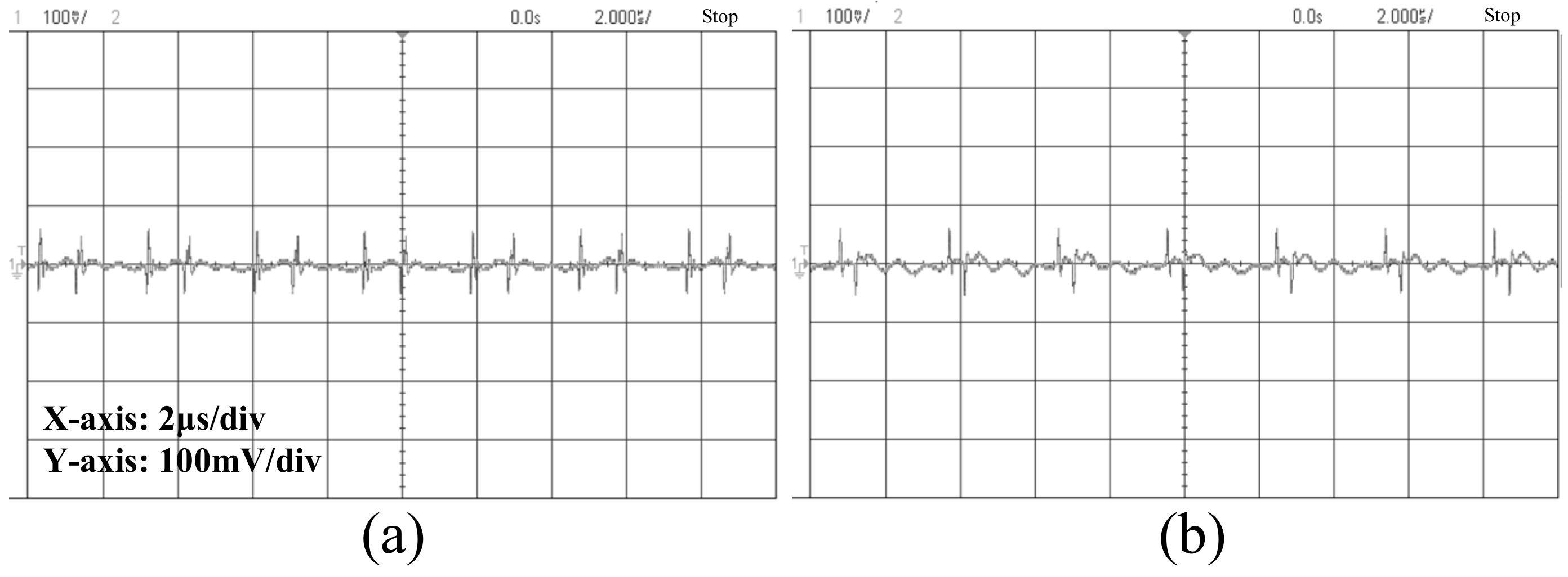
5.2. Transient, Ripple, and Regulation

The load-transient output voltage waveform is shown in Figure 12 under 28 V input. The load current switches between 0.5 A and half load, with a 0.6 A/μs slew rate. The circuit switches between DCM and CCM. Because SR switches are disabled, the output voltage is stable. The recovery time is 170 μs, and the maximum voltage overshoot/undershoot is 550 mV.
The output ripple voltages (including switching noise) at light load and full load are shown in Figure 13a,b, under 28 V input. The light-load output ripple voltage is 30 mV; it is 114 mV when noise is considered. The full-load output ripple voltage is 40 mV; it is 106 mV when noise is considered. The experimental value is consistent with the estimated value. The proposed light-load control does not affect the output ripple voltage.
In addition, the test results show that the load regulation (no load to full load) is 43 mV, and the line regulation (input 20 V to 36 V) is 23 mV; thus, the voltage regulation is accurate, which is consistent with the calculation result. According to the test, the stand-by current under no load is 12 mA.

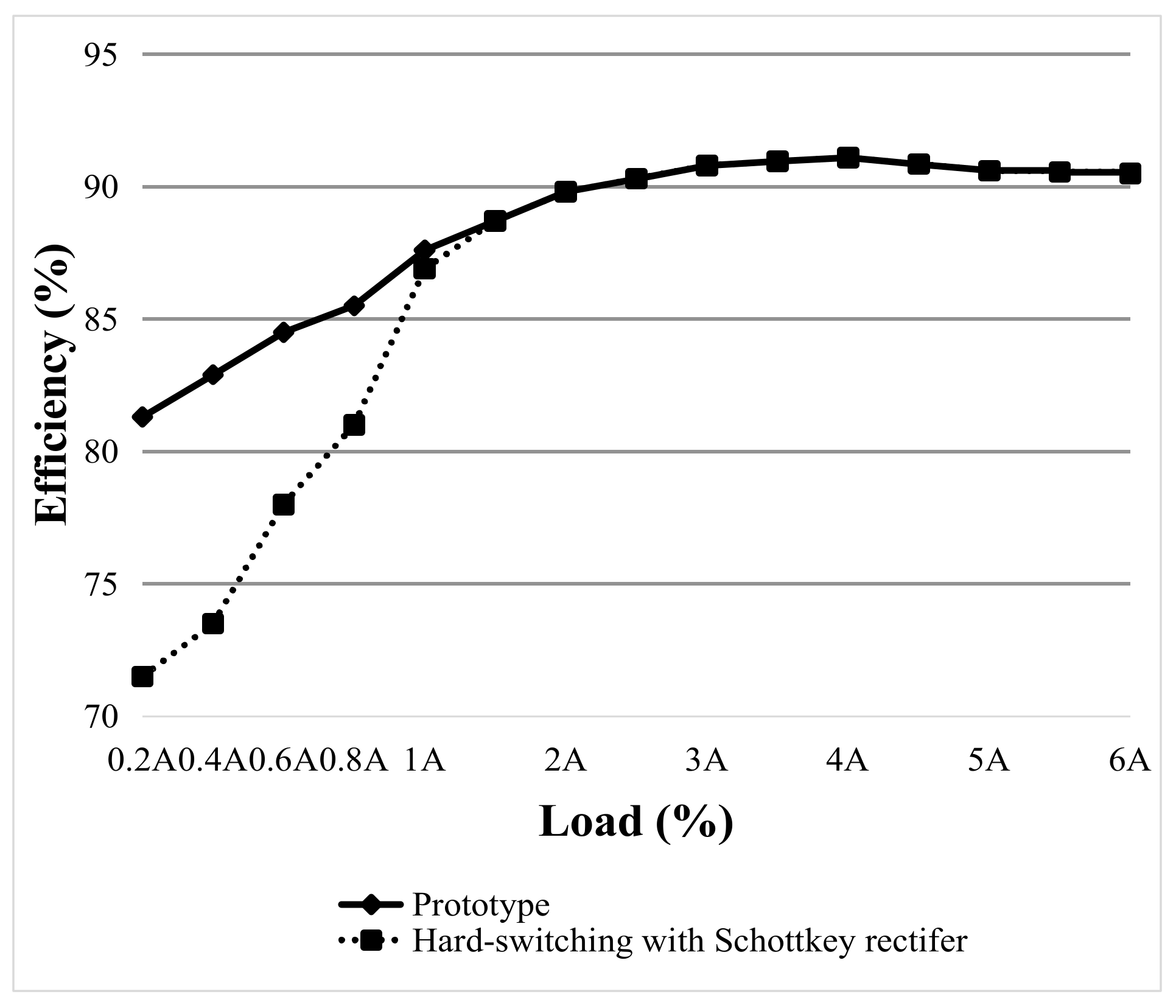
5.3. Efficiency Discussion and Comparison

The efficiency curves at 28 V input are shown in Figure 14. The prototype is compared with the traditional converter, which has hard-switching and Schottky rectification. At 0% to 20% load (0 A to 1.4 A), the efficiency is above 81%, which is 5% to 10% higher than the traditional converter. Especially, the efficiency is 84% at 0.5 A, 9.5% higher than the traditional converter. The result is consistent with the estimated efficiency in Figure 8. It is noteworthy that the control board loss is considered in the efficiency test. Losses of the control board and the power board at light load are shown in Table 3.
The comparison between the proposed circuit and the latest articles is shown in Table 4. Compared with other forward/buck circuits, the prototype does not require additional circuits to achieve light-load soft-switching. It has higher output power compared with flyback circuits. The prototype adopts the derating design and high-grade components, suitable for high-rel applications such as in industry, aerospace, and the military. In addition, the proposed control scheme can also be used in the two-switch forward converter, which can expand the output power further.

6. Conclusions

This paper proposes a digital control method for an isolated regulated converter, which realizes synchronous rectification and soft-switching under DCM. First, the theories of soft-switching in DCM and volt-sec balance are demonstrated. Then, the control scheme is introduced, with the circuit state judgement and configuration program. In the judgement program, SR only operates in the steady state and tZVS is assigned to DTH in DCM, which is 400 ns. Other parameters, including the controller type and the circuit state judgement’s threshold voltage, were designed in detail. The experimental results show that the quasi-ZVS of the primary switch is realized in DCM, and the software voltage–second balance logic turns off SR2 accurately. The light-load efficiency is 5%-10% higher than the traditional forward circuit. The transient response, output ripple, and voltage regulation are consistent with the calculation results, proving that the circuit performs well under both light load and in a transient state. The proposed control scheme has a low component count and high light-load efficiency compared with other papers.

Author Contributions

Conceptualization, investigation, and writing—original draft preparation, C.M.; validation, C.M. and B.L.; supervision, project administration, and writing—review and editing, J.W. and K.W. All authors have read and agreed to the published version of the manuscript.

Funding

This research received no external funding.

Data Availability Statement

The data are contained within the article.

Conflicts of Interest

The authors declare no conflict of interest.

References

  1. Qahouq, J.A.; Abdel-Rahman, O.; Huang, L.; Batarseh, I. On Load Adaptive Control of Voltage Regulators for Power Managed Loads: Control Schemes to Improve Converter Efficiency and Performance. IEEE Trans. Power Electron. 2007, 22, 1806–1819. [Google Scholar] [CrossRef]
  2. Fu, D. Topology Investigation and System Optimization of Resonant Converters. Ph.D. Dissertation, Virginia Polytechnic Institute and State University, Blacksburg, VA, USA, 4 February 2010. [Google Scholar]
  3. ENERGY STAR Program Requirements for External Power Supplies (Version 2.0), U.S. Environmental Protection Agency. Available online: http://www.energystar.gov/ (accessed on 22 December 2022).
  4. Olivier, T.; Yue, W. A Survey of Light-Load Efficiency Improvement Techniques for Low-Power DC-DC Converters. In Proceedings of the International Conference on Power Electronics-ECCE Asia, Jeju, Republic of Korea, 30 May–3 June 2011. [Google Scholar]
  5. Jitaru, I. 99% efficiency DC-DC converter. In Proceedings of the IEEE International Telecom Energy Conference, Vancouver, BC, Canada, 28 September–2 October 2014. [Google Scholar]
  6. Zhou, X.W.; Donati, M. Improved Light-load Efficiency for Synchronous Rectifier Voltage Regulator Module. IEEE Trans. Power Electron. 2000, 15, 826–834. [Google Scholar] [CrossRef]
  7. Le, H.N.; Sato, D.; Orikawa, K.; Itoh, J.I. Efficiency Improvement at Light Load in Bidirectional DC-DC Converter by Utilizing Discontinuous Current Mode. In Proceedings of the European Conference on Power Electronics and Applications, Geneva, Switzerland, 8–10 September 2015. [Google Scholar]
  8. Geng, M.; Feng, Q. Design of A Synchronous Rectifier Controller for Limiting Reverse Current. In Proceedings of the Asia-Pacific Power and Energy Engineering Conference, Wuhan, China, 27–31 March 2009. [Google Scholar]
  9. LT8311 Synchronous Rectifier Controller with Opto-Coupler Driver for Forward Converters, Analog Devices. Available online: https://www.analog.com/ (accessed on 20 December 2022).
  10. Chang, W.H.; Chen, Y.M.; Chen, C.J.; Wang, P.Y.; Lin, K.Y.; Lee, C.C.; Lo, L.D.; Lin, J.Y.; Yang, T.Y. Highly Integrated ZVS Flyback Converter ICs With Pulse Transformer to Optimize USB Power Delivery for Fast-Charging Mobile Devices. IEEE J. Solid-State Circuits 2020, 55, 3189–3199. [Google Scholar] [CrossRef]
  11. Vratislav, M. Inductor Current Zero-Crossing Detector and CCM/DCM Boundary Detector for Integrated High-Current Switched-Mode DC–DC Converters. IEEE Trans. Power Electron. 2014, 29, 5384–5391. [Google Scholar]
  12. Rodriguez, M.; Lamar, D.G. A Novel Adaptive Synchronous Rectification System for Low Output Voltage Isolated Converters. IEEE Trans. Ind. Electron. 2010, 58, 3511–3520. [Google Scholar] [CrossRef]
  13. UCC24636 Synchronous Rectifier (SR) Controller with Ultra-Low Standby Current, Texas Instruments. Available online: https://www.ti.com/ (accessed on 9 July 2022).
  14. XDPS21071 Forced Frequency Resonant Flyback Controller, Infineon Technologies. Available online: https://www.infineon.com/cms/en/ (accessed on 9 July 2022).
  15. Jitaru, I.; Savu, A.; Jitaru, B. Ideal Flyback Topology. In Proceedings of the International Exhibition and Conference for Power Electronics and Intelligent Motion, Nürnberg, Germany, 4–6 May 2021. [Google Scholar]
  16. Zhang, J.; Huang, X. A High Efficiency Flyback Converter With New Active Clamp Technique. IEEE Trans. Power Electron. 2010, 25, 1775–1785. [Google Scholar] [CrossRef]
  17. Tong, Q. A Soft-switching Step Down Converter for Point of Load Applications. In Proceedings of the IEEE International Conference on Electronics Technology, Chengdu, China, 8–12 May 2020. [Google Scholar]
  18. Ahn, M.; Park, J.H. An Optimal Control Method of Clamp Switch for ZVS Bi-directional DC-DC Converter. In Proceedings of the IEEE International Power Electronics and Motion Control Conference, Hefei, China, 22–26 May 2016. [Google Scholar]
  19. Knecht, O.; Bortis, D.; Kolar, J.W. ZVS Modulation Scheme for Reduced Complexity Clamp-Switch TCM DC-DC Boost Converter. IEEE Trans. Power Electron. 2018, 33, 4204–4214. [Google Scholar] [CrossRef]
  20. Ulrich, B. Analysis and Design of a ZVS Clamp-Switch SEPIC DC/DC Converter. In Proceedings of the IEEE Applied Power Electronics Conference and Exposition, New Orleans, LA, USA, 15–19 March 2020. [Google Scholar]
  21. Park, J.; Moon, Y.J.; Jeong, M.G.; Kang, J.G.; Kim, S.H.; Gong, J.C.; Yoo, C. Quasi-Resonant (QR) Controller with Adaptive Switching Frequency Reduction Scheme for Flyback Converter. IEEE Trans. Ind. Electron. 2016, 63, 3571–3581. [Google Scholar] [CrossRef]
  22. Khorasani, R.R.; Adib, E.; Farzanehfard, H. ZVT Resonant Core Reset Forward Converter With a Simple Auxiliary Circuit. IEEE Trans. Ind. Electron. 2018, 65, 242–250. [Google Scholar] [CrossRef]
  23. Soltanzadeh, K. Zero-current Transition Single-ended Forward Converter. IET Power Electron. 2020, 13, 1227–1235. [Google Scholar] [CrossRef]
  24. Chen, G.; Deng, Y.; Chen, L.; Hu, Y.; Jiang, L.; He, X.; Wang, Y. A Family of Zero-Voltage-Switching Magnetic Coupling Nonisolated Bidirectional DC–DC Converters. IEEE Trans. Ind. Electron. 2017, 64, 6223–6233. [Google Scholar] [CrossRef]
Figure 1. (a) Forward circuit with synchronous rectifiers. and (b) inductor current and gate-drive signal in continuous conduction mode and discontinuous conduction mode.
Electronics 12 00575 g001
Figure 2. Key voltage and current waveforms of the proposed circuit.
Electronics 12 00575 g002
Figure 3. Equivalent circuits of each mode. (a) Mode 1 (t0t1); (b) mode 2 (t1t2); (c) mode 3 (t2t3); (d) mode 4 (t3t4); (e) mode 5 (t4t0).
Electronics 12 00575 g003
Figure 4. The proposed control diagram in DCM.
Electronics 12 00575 g004
Figure 5. The control flow chart in DCM.
Electronics 12 00575 g005
Figure 6. The workflow of circuit state judgement and configuration.
Electronics 12 00575 g006
Figure 7. The waveform and generation of PWM signals.
Electronics 12 00575 g007
Figure 8. Estimated power loss comparison between the prototype and the traditional forward converter at 0.5 A load and 28 V input.
Electronics 12 00575 g008
Figure 9. The prototype and environment.
Electronics 12 00575 g009
Figure 10. Gate-drive signal Vgs(S), Vgs(SR1), and Vgs(SR2); inductor current waveforms ILo at (a) 28 V input, 0.3 A load; (b) 28 V input, 0.9 A load; (c) 20 V input, 0.2 A load; (d) 20 V input, 0.7 A load; (e) 36 V input, 0.4 A load; (f) 36 V input, 1 A load. (X-axis: 800 ns/div; Y-axis: Vgs(S)/Vgs(SR1)/Vgs(SR2): 10 V/div, ILo: 1 A/div). The small symbol “T” is the zero position of the time axis.
Electronics 12 00575 g010
Figure 11. Drain-source voltage and gate-driver voltage of the primary switch at (a) 28 V input; (b) 20 V input; and (c) 36 V input. (X-axis: 400 ns/div; Y-axis: Vds(S): 20 V/div; Vgs(S): 10 V/div). The small symbol “T” is the zero position of the time axis.
Electronics 12 00575 g011
Figure 12. The output voltage waveform under load-step transient from 0.5 A to half load.
Electronics 12 00575 g012
Figure 13. The output voltage ripple under (a) 0.5 A load and (b) full load.
Electronics 12 00575 g013
Figure 14. Efficiency comparison between the prototype and traditional forward converter at 28 V input.
Electronics 12 00575 g014
Table 1. Comparison with other SR forward controllers.
Controller Type (Company)Price (Source: DigiKey)Released YearDescription
dsPIC33CK32MP502 (Microchip)US$3.42018Twenty-Eight-Pin Digital Signal Controllers with High-Resolution PWM
LTC3726 (ADI)US$5.82008Secondary-Side Synchronous Forward Controller
LTC3766 (ADI)US$112016High Efficiency Secondary-Side Synchronous Forward Controller
SC4910A (Semtech)US$2.52005Current-Mode PWM Controller with Complementary Output
Table 2. Key parameters of the prototype.
ParametersValue
Input voltage (Vi)20 V to 36 V (28 V typical)
Output voltage (VO)15 V
Maximum output power (PO)100 W
Switching frequency (fs)350 kHz
Transformer turns ratio (N)3:5
Output inductance (LO)12 μH
Magnetizing inductance (Lm)33 μH
Output capacitance (CO)110 μF
Transformer leakage inductance (Lk)0.1 μH
Current transformer turns ratio (NS)100:1
Sampling resistor (RS)22 Ω
Table 3. Loss and efficiency test results at light load.
Total Input Power (@ Load Current)Power Board LossControl Board LossTotal Efficiency
3.7 W (0.2 A)0.4 W0.29 W81.3%
7.3 W (0.4 A)0.94 W0.3 W82.9%
10.7 W (0.6 A)1.34 W0.31 W84.5%
14 W (0.8 A)1.73 W0.31 W85.5%
17.1 W (1 A)1.81 W0.31 W87.6%
Table 4. Comparison with other soft-switching converters.
Author, YearTopologyAdditional Component CountLight-Load Efficiency, (Load Range)Maximum Output PowerApplication Fields
This paperSR forward081–87%, (0–20%)100 WIndustry, aerospace, military
[10], 2020Flyback082–88%, (0–30%)60 WFast-charging
[21], 2016Flyback084.9–87.4%, (8–25%)40 WFast-charging
[22], 2018Forward>2, ZVT circuit<86%, (<20%)150 WHome appliances, industry
[23], 2020Forward>3, ZCT circuit<86%, (<20%)200 WMedical, industry
[24], 2017Buck>3, ZVS circuit<91%, (<20%)500 WIndustry
Disclaimer/Publisher’s Note: The statements, opinions and data contained in all publications are solely those of the individual author(s) and contributor(s) and not of MDPI and/or the editor(s). MDPI and/or the editor(s) disclaim responsibility for any injury to people or property resulting from any ideas, methods, instructions or products referred to in the content.

