Article

An Enhanced Detection Method of PCB Defect Based on D-DenseNet (PCBDD-DDNet)

School of Information Management, Beijing Information Science and Technology University, Beijing 100192, China
*
Author to whom correspondence should be addressed.
Electronics 2023, 12(23), 4737; https://doi.org/10.3390/electronics12234737
Submission received: 26 August 2023 / Revised: 17 November 2023 / Accepted: 20 November 2023 / Published: 22 November 2023
(This article belongs to the Special Issue Deep Learning in Multimedia and Computer Vision)

Abstract

:
Printed Circuit Boards (PCBs), as integral components of electronic products, play a crucial role in modern industrial production. However, due to the precision and complexity of PCBs, existing PCB defect detection methods exhibit some issues such as low detection accuracy and limited usability. In order to address these problems, a PCB defect detection method based on D-DenseNet (PCBDD-DDNet) has been proposed. This method capitalizes on the advantages of two deep learning networks, CDBN (Convolutional Deep Belief Networks) and DenseNet (Densely Connected Convolutional Networks), to construct the D-DenseNet (Combination of CDBN and DenseNet) network. Within this network, CDBN focuses on extracting low-level features, while DenseNet is responsible for high-level feature extraction. The outputs from both networks are integrated using a weighted averaging approach. Additionally, the D-DenseNet employs a multi-scale module to extract features from different levels. This is achieved by incorporating filters of sizes 3 × 3, 5 × 5, and 7 × 7 along the three paths of the CDBN network, multi-scale feature extraction network, and DenseNet network, effectively capturing information at various scales. To prevent overfitting and enhance network performance, the Adafactor optimization function and L2 regularization are introduced. Finally, online hard example mining mechanism (OHEM) is incorporated to improve the network’s handling of challenging samples and enhance the accuracy of the PCB defect detection network. The effectiveness of this PCBDD-DDNet method is demonstrated through experiments conducted on publicly available PCB datasets. And the method achieves a mAP (mean Average Precision) of 93.24%, with an accuracy higher than other classical networks. The results affirm the method’s efficacy in PCB defect detection.

1. Introduction

Printed Circuit Boards (PCBs), as crucial components that connect electronic parts and form circuits, play an important role in the performance of related electronic products [1]. Due to the intricate craftsmanship and precise wiring of PCBs, coupled with the rapid development of integrated circuits, PCBs are becoming more integrated and compact. Consequently, the existing defects are becoming harder to detect, posing challenges in PCB defect inspection [2]. With the rapid growth of the electronic industry, the application of PCBs in electronic products is becoming increasingly extensive [3]. However, owing to various factors in the manufacturing process, various defects such as open circuits, short circuits, and poor soldering may occur on PCBs. These defects can impact the quality and performance of electronic products, and even lead to product malfunctions. Therefore, the rapid and accurate detection of PCB defects has become a crucial issue in the electronic industry [4].
Traditional PCB defect detection can be primarily categorized into three major types [5]: manual visual inspection, electrical testing, and optical inspection. Manual visual inspection involves workers directly examining PCB bare boards using the naked eye and other auxiliary equipment. Griffin et al. [6] utilized an 80,386 microprocessor for defect detection, capable of identifying defects such as open circuits, partial open circuits, short circuits, and surface imperfections. PutemS et al. [7] employed a reference-based method in MATLAB to generate defect group images containing only defects, achieving a finer segmentation of defects. Li et al. [8] processed PCB images through bilateral filtering and employed feature vectors and support vector machine classifiers to recognize and locate four classes of defects. However, as PCBs move towards higher levels of precision, this method suffers from drawbacks such as poor detection stability and low efficiency, making it unsuitable for the current PCB defect detection requirements.
Subsequently, electrical testing methods have emerged that utilize the electrical characteristics of components to detect PCB defects [9]. This approach involves a semi-automated manual testing method, including online testing and functional testing [10]. Kuang Yongcong et al. [11] performed statistical analysis on good and defective samples, combined with minimum risk Bayesian decision-making to classify defect characteristics, reducing the workload for developers. Gaidhane et al. [12] applied traditional machine learning algorithms for PCB defect detection. Annaby et al. [13] proposed a low-complexity NNC traditional machine vision solution to address defect detection issues. Tsai et al. [14] utilized Fourier image reconstruction methods to detect minor defects. Cho J W et al. [15] achieved real-time defect detection using ultrasonic laser thermography, which can reduce costs when compared with manual detection methods. However, limitations like the non-reusability of the testing process, high testing equipment costs, and complex function programming have restricted its application.
To address the surface inspection of products, some foreign electronics manufacturers have introduced Automated Optical Inspection (AOI), a machine vision-based automated optical detection technology, for the detection of surface defects on PCBs [16,17]. This involves capturing images of the product’s surface using cameras and light sources, followed by encoding, analyzing, and quantifying the image features using image algorithms. This process enables the extraction and detection of defect characteristics. In comparison to contact-based inspection methods [18], AOI technology offers a higher efficiency for PCB defect detection [19], without causing damage to the PCB during the inspection process, making it a primary detection method. In 2011, Ajay Pal et al. compared standard PCB images with images of the PCBs that were required to be tested. They used a subtraction algorithm to detect typical defects such as open circuits, short circuits, and holes in PCB bare boards [20]. In 2014, Malge P.S. and colleagues employed morphological image segmentation algorithms to detect defects on single-layer PCB bare boards. They used simple image processing techniques for defect classification and localization [21]. In 2015, Swagata Ray et al. proposed a hybrid detection method involving image representation, comparison, and segmentation algorithms. Experimental results demonstrated that this method not only classifies and locates defects in PCBs but also achieves a higher accuracy of detection [22]. In 2016, Neelum Dave et al. employed a method of comparing the PCB images required to be tested with template images to detect defects. During the detection process, they extracted structural features of defects based on attributes like perimeter, area, and orientation, enabling accurate defect detection in PCBs [23]. However, AOI systems require precise setup and calibration, which demand specialized knowledge and experience, and it takes a substantial amount of time to adjust the system to accommodate various PCB designs and manufacturing requirements.
Compared to traditional machine vision-based methods, deep learning algorithms possess powerful nonlinear capabilities, making them suitable for handling more complex scenarios and exhibiting a higher robustness. Among these approaches, Huang et al. [24] improved the classification capability of the convolutional neural network when labeled data are scarce. Zhuang et al. [25] made enhancements to the Faster R-CNN network by incorporating a deep transfer network, resulting in an improved classification performance of the algorithm. Chen Xiang et al. [26] employed Convolutional Neural Networks for the classification and recognition of electronic components on circuit boards. Wang Yongli et al. [27] introduced a deep learning-based method for the recognition and classification of 10 types of defects including open circuits, burrs, and excess copper on PCB pads and traces. Hu et al. [28] utilized Faster R-CNN to detect minor defects on circuit boards, employing ResNet50 as the backbone network for feature extraction. To better detect small defects on PCBs, they used the GARPN module for accurate anchor prediction, followed by merging with ShuffleNetV2 residual units, achieving a high accuracy. Chen Wenshuai [29] addressed the orientation issue of polar electronic components, employing Faster R-CNN and YOLOv3 networks for the classification, orientation recognition, and localization of polar devices. This method significantly improved accuracy and timeliness compared to traditional algorithms. Wu Jigang et al. [30] introduced an improved YOLOv4 network, which first determined pre-selected boxes in PCB images, and subsequently used MobileNetV3 and Inceptionv3 networks for feature extraction and detection, respectively. Hu Shanshan et al. [31] proposed a network called UF-Net, achieving the accurate identification of various defects on circuit boards such as traces and solder joints through feature upsampling, fusion, Region Proposal Network (RPN), and ROI pooling modules.
The multimodal methods and feature extraction techniques used in the marketing intent analysis of social media advertising are equally applicable to PCB defect detection [32]. Liu et al. [33] presented a new method using the principle of multimodal deep learning-based one-class novelty detection to support AOIs and operators to detect defects more accurate or to determine whether something needs to be changed. Lu et al. [34] extracted the histogram of oriented gradients and local binary pattern features for each PCB image, respectively, by inputting into a support vector machine to obtained two independent models. Then, according to Bayes fusion theory, the authors fused two models for defect classification. The robustness of deep learning models when faced with abnormal or defective PCB images can be enhanced through adversarial training [35]. Adversarial training involves introducing adversarial samples into the training data. These samples are intentionally designed to deceive the model, enabling it to remain effective in the presence of different types of defects or anomalies. This means introducing adversarial samples during model training to ensure its effectiveness when facing various types of defects or anomalies [36,37,38]. Hashing is an efficient method for nearest neighbor search in large-scale data space by embedding high-dimensional feature descriptors into a similarity preserving Hamming space with a low dimension [39]. Based on comparison between image signatures (hashcode), the authors of [40] present a method of PCB inspection. Image hash is extracted resistant to geometric distortions. The extracted hash is used to identify the component and related defects including missing component, mistake component, and inverse orientation. By applying these techniques to PCB images and relevant information, the system can more accurately identify and analyze PCB defects, improving detection efficiency and accuracy.
As can be gleaned from the above, traditional methods and machine vision approaches can, to a certain extent, be utilized for PCB defect detection. However, these methods struggle to meet the demands of the modern PCB manufacturing industry for high-speed, high-precision quality inspection [41]. Currently, PCB defect detection methods based on deep learning technology have shown some improvements in detection performance, but they still have limitations. For instance, some deep learning models may perform well under specific PCB board or environmental conditions, but their generalization performance could be poorer when applied to different boards or environments. Additionally, when dealing with rare defect types, deep learning models may encounter the problem of small sample sizes, making it challenging to adequately learn these cases. Based on these factors, this paper focuses on a deep learning-based PCB defect detection method, constructing a PCB defect detection model to further enhance the accuracy of circuit board defect detection. The main contributions of this paper are as follows:
(1)
To address the issues of low detection accuracy, difficulty in detecting small defects, and limited usability in existing PCB inspection methods, a PCB defect detection method based on D-DenseNet (PCBDD-DDNet) is proposed in this paper.
(2)
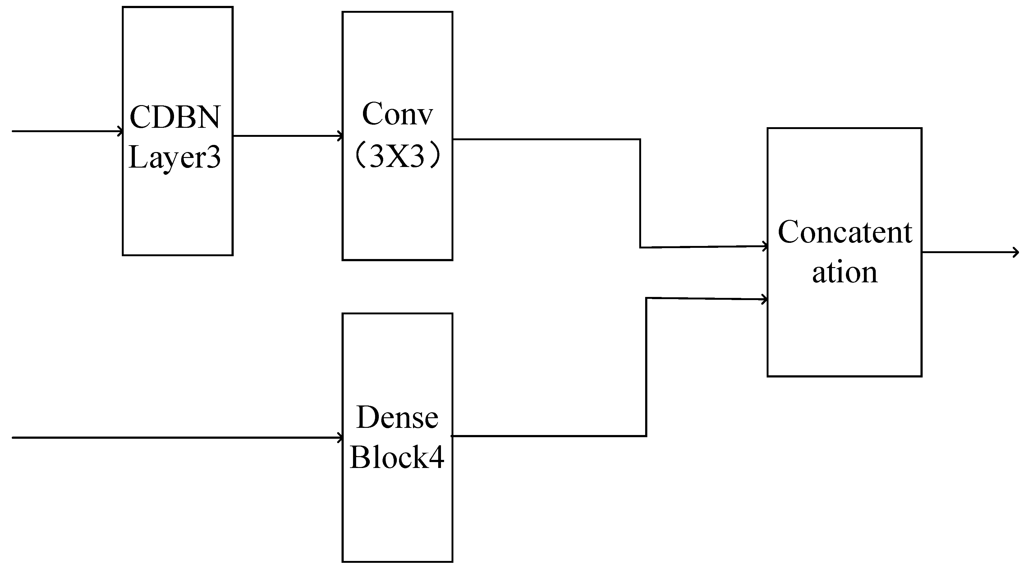
The D-DenseNet model that combines two powerful deep neural networks, CDBN and DenseNet, is proposed. It employs the output of the third layer from CDBN as the input for DenseNet. Following the fourth Dense Block of DenseNet, a concatenation layer is introduced to merge the low-level features extracted by CDBN with the high-level features extracted by DenseNet. This further enhances the model’s performance.
(3)
A multi-scale feature extraction module is used to extract feature maps at different levels of the network. Filters of sizes 3 × 3, 5 × 5, and 7 × 7 are added on three paths in the CDBN network, multi-scale feature extraction network, and DenseNet network, respectively, to effectively capture information at different scales. Subsequently, 1 × 1 convolutional kernels are employed to merge these features for feature extraction and classification purposes.
By integrating CDBN with DenseNet networks, adding multi-scale feature extraction module, and introducing Adafactor optimization function and L2 regularization, the aim is to monitor and evaluate the security status of the network in real time through deep learning methods, and to improve the security and reliability of the network.
Deep Learning (DL) has been proven effective in processing and analyzing visual media [42]. Deep learning has garnered significant research interest in many applications of Artificial Intelligence (AI), such as image understanding, object detection, feature extraction, audio/video processing, image denoising and deblurring, and defect detection in industrial applications [43]. Deep learning has become a key technology in the field of multimedia computing. It provides a powerful tool for generating high-level abstractions of complex multimedia data, applicable in various applications including object detection and recognition, speech-to-text, media retrieval, multimodal data analysis, and more [44]. Convolutional Neural Networks demonstrate high capabilities in image recognition and classification, and deep learning tailored for intelligent multimedia analysis is emerging as a burgeoning research area in multimedia and computer vision [45]. This study’s primary contributions to multimedia-related research are as follows:
(1)
By introducing a combination of deep learning network structures (CDBN and DenseNet), this method achieves high accuracy and comprehensive feature extraction in PCB defect detection. This technical contribution indicates the application of deep learning in the field of multimedia, especially in image processing and analysis, playing a crucial role in industrial production. This provides strong support for the practical application of multimedia technology in manufacturing, expanding its scope in industrial production.
(2)
The introduction of a multi-scale module extracts image features through filters of different scales. This innovative application is particularly important in the multimedia field, emphasizing the importance of considering multiple levels and scales in image analysis. This not only achieves good results in PCB defect detection but also provides insights for image analysis in other multimedia fields, potentially advancing the development of multimedia technology in various application areas.
(3)
Through experimentation on publicly available PCB datasets, the method demonstrates significant achievements in PCB defect detection, with a mean Average Precision (mAP) reaching 93.24%, and accuracy surpassing other classical networks. This indicates the high efficiency of the method in practical applications. From a practical application perspective, this technical contribution provides an efficient and accurate method for PCB defect detection in manufacturing. It is expected to be widely applied in the field of electronic product manufacturing, contributing to improved quality control and reduced defect rates, thereby enhancing the competitiveness of the entire manufacturing industry.
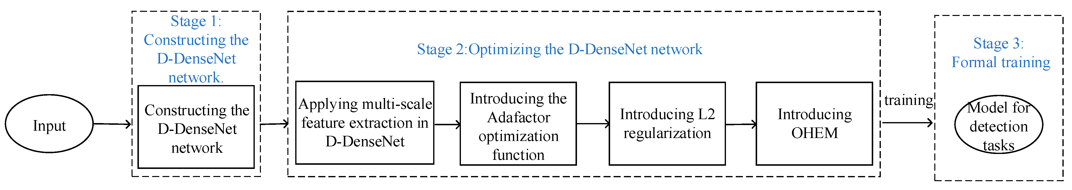
2. Methods

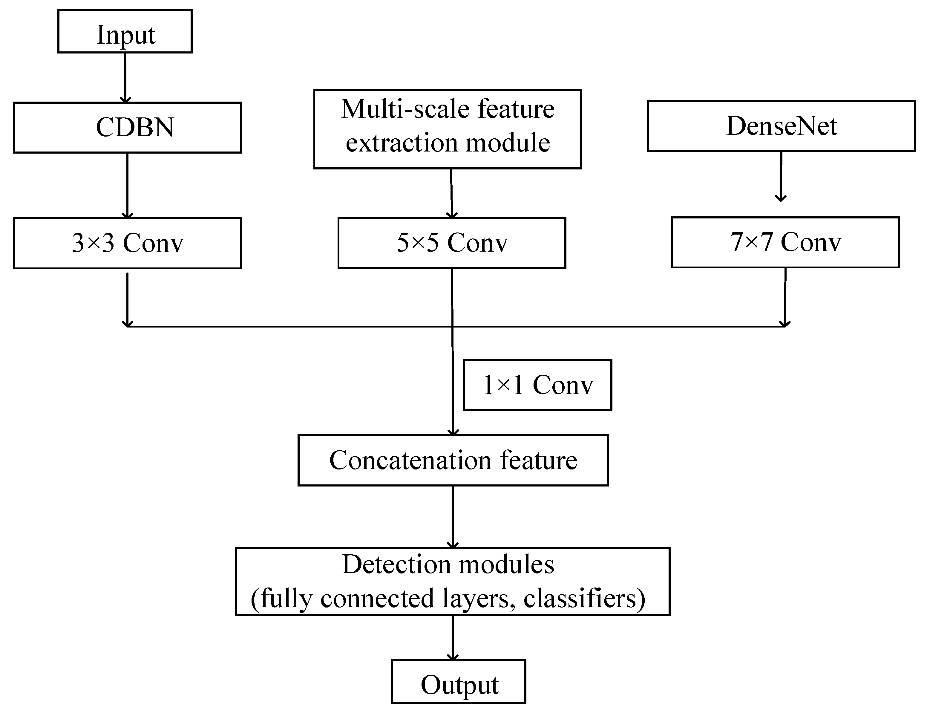
2.1. Design of PCBDD-DDNet

To address the challenges of low detection accuracy and limited usability in existing PCB inspection methods, we propose a PCB defect detection method based on the D-DenseNet network (referred to as PCBDD-DDNet). This method leverages the strengths of two deep learning networks, CDBN and DenseNet, to construct the D-DenseNet network. In this network, CDBN is responsible for extracting low-level features, while DenseNet focuses on high-level feature extraction, and their outputs are integrated through weighted averaging. Furthermore, the D-DenseNet incorporates a multi-scale module to extract features from different levels, effectively capturing information at various scales. The introduction of the Adafactor optimization function and L2 regularization helps prevent overfitting and improves network performance. Lastly, the Online Hard Example Mining (OHEM) mechanism is introduced to enhance the network’s ability to handle difficult samples, thereby improving the accuracy of PCB defect detection.
The core idea of the PCBDD-DDNet method is to leverage the strengths of the deep learning networks, CDBN and DenseNet. It constructs the D-DenseNet network, where CDBN is utilized for extracting low-level features, and DenseNet is responsible for high-level feature extraction. The network outputs are integrated through weighted averaging, and a multi-scale module is introduced, incorporating 3 × 3, 5 × 5, and 7 × 7 filters to effectively capture information at different scales. Key components of the learning framework include CDBN, DenseNet, multi-scale module, Adafactor optimization function, L2 regularization, and Online Hard Example Mining (OHEM) mechanism. These components collectively form the learning framework of PCBDD-DDNet.
The overall process of PCBDD-DDNet is illustrated in Figure 1. It consists of three main phases: stage 1, construction of the D-DenseNet network; stage 2, optimization of the D-DenseNet network, involving the application of a multi-scale module, introduction of the Adafactor optimization function and L2 regularization, and integration of the OHEM mechanism; and stage 3, training of the preprocessed data based on the constructed D-DenseNet network, resulting in a model that can be employed for detection tasks.
In the stage 1 of constructing the D-DenseNet network, on the one hand, this network employs the first three layers of the CDBN network to compute the size of its output feature map and flattens it into a one-dimensional vector. Then, convolutional layers are used to transform the output of CDBN into a three-dimensional feature map, which is served as the input to DenseNet. The output dimensions are set to match the input channels of the first Dense Block of DenseNet. Finally, the output of the convolutional layers is concatenated with the input to the first Dense Block of DenseNet to fuse deep features. On the other hand, to further enhance network performance, this network adds a concatenation layer after the fourth Dense Block of DenseNet, fusing high-level features from CDBN with low-level features from DenseNet. This approach leads to a more comprehensive feature representation and improves the network’s expressive power and classification performance.
In stage 2, for better guiding the network to learn useful features, a multi-scale feature extraction module is introduced. Features are extracted from the input using filters of different sizes, with filter sizes of 3 × 3, 5 × 5, and 7 × 7 for the CDBN network, multi-scale feature extraction network, and DenseNet network paths, respectively. Subsequently, features are fused using 1 × 1 convolutional kernels and introduced with nonlinearity. Utilizing filters of different sizes enables the extraction of information from the input image at various scales. Moreover, the network employs the Adafactor optimization function and L2 regularization. Adafactor is an adaptive optimization algorithm that automatically adjusts the learning rate, considering historical gradients for each parameter. This approach helps the network converge more stably and achieve better classification performance, further enhancing the network’s performance and robustness. L2 regularization mitigates the risk of overfitting. Additionally, the PCBDD-DDNet method introduces the Online Hard Example Mining (OHEM) mechanism to improve the handling of difficult samples and enhance the accuracy of PCB defect detection.
In stage 3, preprocessed PCB image data are fed into the D-DenseNet network for training, resulting in a model suitable for PCB defect detection tasks.

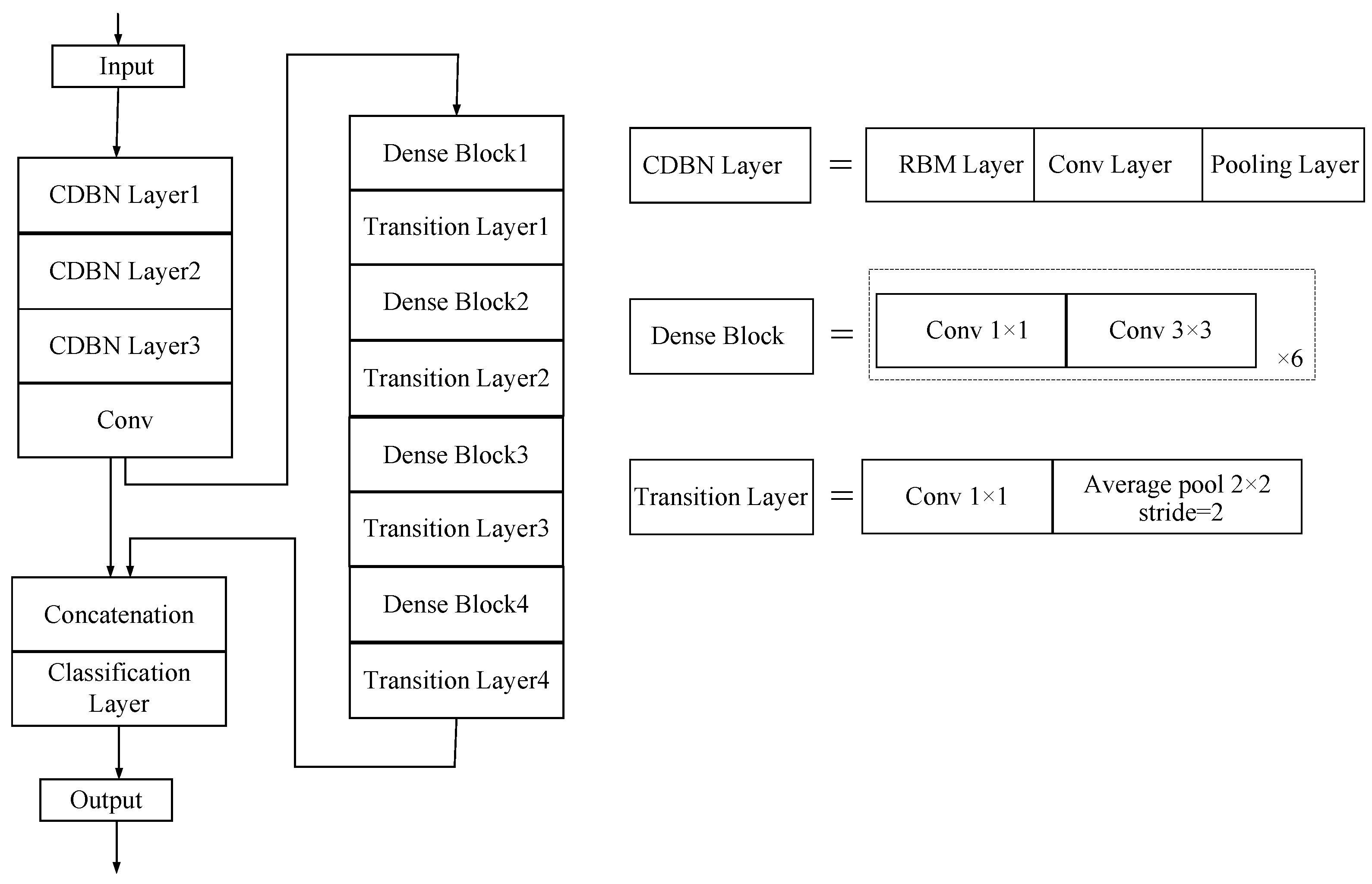
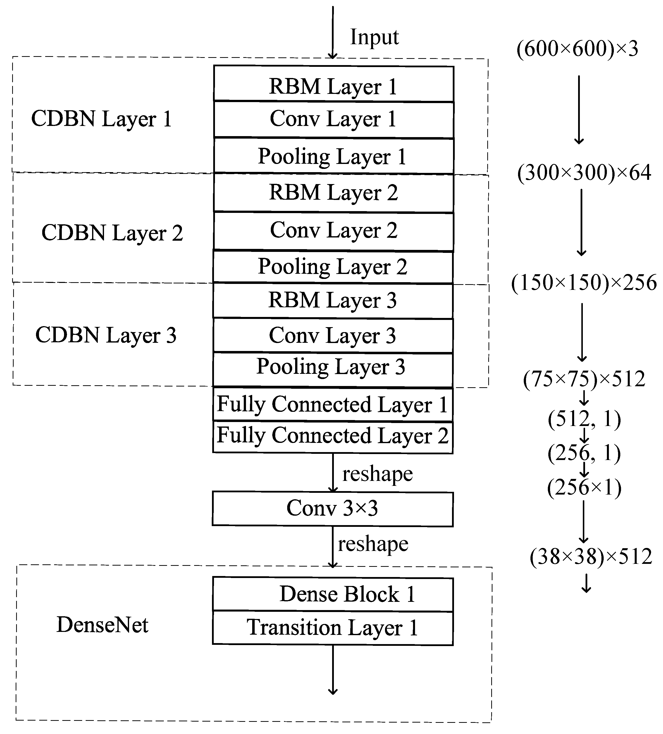
2.2. Constructing the D-DenseNet Network

DBN (Deep Belief Networks) [46] is a deep learning model composed of multiple layers of RBM (Restricted Boltzmann Machines [47]), commonly used for unsupervised learning and feature extraction. The CDBN (Convolutional Deep Belief Network) combines the strengths of RBM and CNN (Convolutional Neural Networks) and aims to handle data with grid-like structures, such as image data. It employs a hierarchical structure, with each layer consisting of both RBM and CNN components.
DenseNet is a Deep Convolutional Neural Network that can better reuse features and parameters. It was proposed by Huang et al. in 2017 [48]. The main feature of DenseNet is dense connections, where all feature maps of the previous layer are connected to the current layer’s input. This connection significantly alleviates the problem of gradient vanishing, improves the efficiency of information propagation, and helps to learn features better, reducing the occurrence of gradient vanishing problem and improving the network’s training and generalization capabilities.
The construction of the D-DenseNet network involves the integration of two powerful deep neural networks, namely, the Convolutional Deep Belief Network (CDBN) and DenseNet, with the aim of extracting more image features and enhancing the network’s detection performance. The network architecture of D-DenseNet is illustrated in Figure 2.

2.2.1. Data Dimension Transformation

Because the CDBN and DenseNet networks accept input data of different dimensions, it is necessary to perform dimensionality transformation of the data entering the D-DenseNet network to ensure that both the CDBN and DenseNet networks can process the input. Firstly, the preprocessed dataset is used as the input for the entire D-DenseNet network. The data are represented in the form of a two-dimensional matrix, where each element corresponds to the pixel value of the image. For the output data of CDBN, an additional channel is introduced while simultaneously applying zero-padding. Then, a 3 × 3 convolutional layer is introduced, with the convolution kernel sliding over the CDBN output data. For each position, it extracts information from the original channels and computes values for the new channel, thus transforming the output of the CDBN layer into a three-dimensional feature map. Subsequently, this transformed three-dimensional feature map is inputted into the DenseNet network to ensure that both the CDBN and DenseNet layers share the same dimensions and semantics.

2.2.2. Network Integration

CDBN extracts multi-level abstract features from the original input, where the features in the earlier layers are more fundamental and general. Using these features as input for DenseNet enhances its perception and expressive capabilities towards lower-level features, thus improving the network’s performance. Therefore, in this paper, the first three layers of CDBN are employed as input for DenseNet. Specifically, the output feature map size of the third layer in CDBN is computed and flattened into a one-dimensional vector. A 3 × 3 convolutional layer is then utilized to transform the output of CDBN into a three-dimensional feature map, serving as input for the first Dense Block of DenseNet. The output dimensions are set to match the input channel count of the first Dense Block. Finally, the output of the convolutional layer is concatenated with the input of the first Dense Block using the concatenate method, resulting in the network fusion termed D-DenseNet. The network fusion is illustrated in Figure 3.
When concatenating the output of the CDBN with the input of the DenseNet, it is essential to ensure that the output dimensions of the CDBN network align with the input dimensions of the DenseNet network. As a result, the D-DenseNet network adds a convolutional layer after the output layer of the CDBN network to adjust the output dimensions accordingly. Generally, smaller convolutional kernels like 3 × 3 are better suited for capturing local features, while larger kernels like 5 × 5 or 7 × 7 are more effective for capturing global features [49]. Concerning PCB defects, it is important to consider various types of defects that could exist in the dataset. In such scenarios, smaller convolutional kernels might be more suitable, as defects often manifest in localized regions. Therefore, a convolutional kernel size of 3 × 3 is chosen.

2.2.3. Concatenation of Feature Vectors

DenseNet receives the output of all previous layers in each layer and combines them in a concatenation manner. If the DenseNet network has L layers, the input of the l -th layer includes the output of the previous l − 1 layers. This connection method can be represented as follows:
X l = H l [ X 0 , X 1 , , X l 1 ]
In the equation, X l is the output of layer l , H l is the nonlinear transformation function of layer l , and [ X 0 , X 1 , , X l 1 ] is the concatenation of the outputs of all the previous layers. Therefore, each layer in DenseNet can be seen as a function of all the previous layers, with the concatenated outputs of all the previous layers as its input.
The number of parameters in the first layer of DenseNet is calculated as follows:
K l = K 0 + k × ( l 1 )
where K 0 is the initial number of channels, k is the growth rate per layer, and l is the layer.
When concatenating CDBN and DenseNet, it is important to ensure that they share the same feature space. To achieve consistency between the feature spaces of these two networks, fine-tuning is applied to the CDBN. This ensures that the output features of the CDBN align with the input features of the DenseNet. This alignment is achieved by adding an additional convolutional layer to the last layer of the CDBN and fine-tuning it. This convolutional layer transforms the output vector of the CDBN into a feature vector with the same dimensions as the input tensor of the DenseNet. The concatenation of feature vectors is illustrated in Figure 4.
To enable the network to learn richer feature representations and enhance its expressive capacity and classification performance, the D-DenseNet network introduces a concatenation layer after the fourth Dense Block of DenseNet. This layer combines the low-level features extracted by CDBN with the high-level features extracted by DenseNet, thereby further improving the network’s performance.

2.2.4. Construction of the New Network

The concatenated feature vector is used as a new feature vector, which is then inputted into a global average pooling layer to reduce the feature dimensions to one dimension. Subsequently, the feature vector is passed through a fully connected layer for classification. This network combines the strengths of both CDBN and DenseNet to enhance the network’s expressive capability and classification performance, thereby excellently achieving PCB defect detection.
Upon completing the construction of the new network, training and parameter tuning are required. During the training process, data preprocessing is essential to enhance the network’s generalization ability and robustness.

2.3. Multi-Scale Feature Extraction

Multi-scale feature extraction refers to considering feature information of different scales simultaneously in the network [50]. Low-level features are mainly concentrated in the first two layers of convolution. Therefore, a multi-scale module structure is adopted to obtain low-level features from the first two layers and aggregate contextual information at multiple scales to improve learning efficiency. There are two methods for obtaining contextual information in the multi-scale module, i.e., one is by connecting low-level features and high-level features, and the other is by using recursive layers with different dilation rates to extract features at different scales, thus expanding the receptive field. Information in images typically exists across various scales, ranging from low-level features to high-level features.
The effectiveness of the multi-level multi-scale feature extraction network was demonstrated through ablative experiments in reference [51]. In comparison to the simple direct concatenation of low-level features and high-level features, the model based on the multi-level multi-scale feature extraction network proposed in this paper exhibited the best performance. This indicates that the proposed multi-level multi-scale feature extraction network is effective, allowing it to fully leverage the advantages of the multi-level multi-scale feature extraction network in the context of feature extraction. It excels in extracting features at the word level, phrase level, and sentence level to ensure comprehensive feature extraction. Furthermore, it is evident from the literature that retaining only the word-level feature representation module from the multi-level multi-scale feature extraction network results in the poorest model performance. The model’s performance is better when retaining the sentence-level feature extraction module from the multi-level multi-scale feature extraction network as opposed to retaining the word-level feature representation module. The best model performance was achieved by using the complete multi-level multi-scale feature extraction network. This underscores the importance of integrating local feature extraction with global feature extraction when conducting feature extraction, with a particular emphasis on global feature extraction.
The use of recursive layers and filters of different sizes is an effective approach to capture features at different scales, aiding the model in gaining a more comprehensive understanding of the image content. Additionally, it contributes to the model’s improved comprehension of relationships between different regions within the image, thereby enhancing its ability to recognize and locate objects. Hence, this article opts for the second approach to expand the receptive field.
Specifically, the multi-scale module first extracts features from the input using filters of different sizes. The filter sizes for the three paths in the CDBN model, multi-scale feature extraction model, and DenseNet model are 3 × 3, 5 × 5, and 7 × 7, respectively. Then, feature fusion and nonlinearity are introduced using 1 × 1 convolutional kernels. The filters of different sizes instead of different dilation rates are used to extract information from the input data, as filters with larger dilation rates may cause loss of details and decrease the ability to learn better feature representations. The number of filters in the three paths are 12, 20, and 32, totaling 64 feature maps. This combination strikes a balance between feature extraction and parameters, while reducing parameter count by directly connecting feature maps. The network architecture of the multi-scale model is shown in Figure 5.
The input data are first passed through three convolutional layers of the CDBN model to extract low-level features. These low-level features are then passed through the low-level feature path and connected with the features extracted using a 5 × 5 filter in the middle path. The presence of the middle path allows the network to extract features within a moderate receptive field. These features, along with the features extracted using a 7 × 7 filter in the high-level feature path, are fused through concatenation. Finally, all the concatenated features are passed to a detection module, such as a fully connected layer or classifier, for the detection and classification of network attack behaviors.
Multi-scale extraction utilizes feature maps at different levels, where 3 × 3 and 7 × 7 kernels can extract features at different scales in Deep Convolutional Neural Networks. Introducing a filter with a moderate receptive field in the network captures features at an appropriate scale. The presence of the middle path increases the diversity of the network and provides more choices for feature extraction. The inclusion of a multi-scale structure increases the width of the network, on the one hand, and improves the network’s generalization ability, on the other hand.

2.4. Adafactor Optimization Function

Adafactor is an adaptive learning rate optimization algorithm based on the estimation of second-order moments, proposed by SHAZEER et al. in 2018 [52]. The core idea of Adafactor is to use a low-rank approximation of the Fisher information matrix to estimate the second-order moments and regularize the gradient to control the change in learning rate. Unlike other adaptive algorithms, Adafactor uses a grouping approach to update the learning rates of different parameters, which saves storage and computational resources.
The update formula of Adafactor algorithm is as follows:
(1)
Calculate the moving average of the gradient square:
V t + 1 = β 2 v t + ( 1 β 2 ) g t 2
where v t is the moving average of the gradient square at the previous step, β 2 is the decay rate of the moving average, and g t is the gradient at the current time step.
(2)
Calculate the first-order moment estimate of the gradient:
m t + 1 = β 1 m t + ( 1 β 1 ) g t
(3)
Calculate the adaptive learning rate and regularization:
t = α v t + 1 +
ρ t = α v t + 1 + + γ
where α is the learning rate, ∈ is a small constant, and γ is the regularization parameter.
(4)
Calculate the parameter update:
w t + 1 = w t t m t + 1 i m t + 1 ( i ) 2 / ρ t +
where w t + 1 is the updated parameter vector.
The advantages of the Adafactor algorithm are that it can adaptively estimate the second-order moments and learning rates of different parameters without additional learning rate adjustments, improving the efficiency and accuracy of training. In addition, the Adafactor algorithm is suitable for efficient processing of large-scale models and datasets and has a good scalability.

2.5. L2 Regularization

L 2 regularization is a commonly used regularization technique to penalize the weight parameters of a model and prevent overfitting [53]. L 2 regularization adds a penalty term to the model’s parameters, which imposes a higher cost on large parameter values. The size of this penalty term depends on the L 2 norm, also known as the Euclidean norm, of the parameters. Specifically, L 2 regularization restricts the weight parameters of the model by adding the penalty term to the model’s loss function. By limiting the size of the model parameters, L 2 regularization controls the complexity of the model and prevents overfitting on the training data.
Models that use L 2 regularization typically add a regularization term to the loss function, which can be expressed as follows:
L 2 = λ × | w | 2
where λ is the regularization coefficient, and | w | 2 represents the L 2 norm (i.e., the square root of the sum of squares) of the weight vector.
For a linear regression model, the loss function can be expressed as follows:
J w = 1 2 m ( h x i ) y ( i ) 2 + λ 2 m w 2
where w represents the model’s weight parameters, m represents the number of samples, h ( x i ) represents the model’s predicted value, and y ( i ) represents the actual value. The first term is the model’s mean squared error loss, and the second term is the penalty term imposed by L 2 regularization. By adjusting the value of λ, the strength of regularization can be controlled to balance the trade-off between model fitting ability and generalization ability.
In neural networks, L 2 regularization can also be applied to the weight parameters. The loss function can be expressed as follows:
J w = 1 m L y i , y ( i ) + λ 2 m | w | 2
where L y i , y ( i ) is the loss function used to measure the difference between the predicted and actual values, and | w | represents the L 2 norm of the weight parameters, i.e., the square root of the sum of squares of each weight parameter.
L 2 regularization can reduce the complexity of the model and prevent overfitting without compromising its performance. It is particularly useful for handling high-dimensional data, as it effectively controls the model’s complexity and improves its generalization ability.

2.6. Online Hard Example Mining (OHEM)

In PCB defect detection tasks, there is often a large amount of background, and the number of defects is relatively small. This leads to a large number of false positive results during model training, which means that the normal background is incorrectly classified as a defect. To solve this problem, the difficult sample mining mechanism, OHEM, can be introduced to reduce the dominance of false positives on the loss function by setting key parameters of the network [54]. A commonly used method is to set the ratio of positive and negative sample pixels to 1:3.
The specific approach is as follows: first, the training samples are inputted into the network model to obtain the confidence level of each pixel belonging to each category. The pixels belonging to the defect category are selected as positive samples. Then, all remaining negative sample pixels are arranged according to their confidence level, and negative sample pixels are selected in a 1:3 ratio. If the number of positive sample pixels is small, it can be taken from the sorted negative sample pixels as positive samples to meet the requirements of positive samples for pixels.
During the training process, the selection of samples is random and does not consider the impact of simple or difficult samples on model training. However, in PCB defect detection, due to complex textures, the background often produces pixels that are similar to or difficult to distinguish from defects. In order to improve the segmentation effect of PCB defects, it is necessary to address the impact of difficult samples and a large number of simple samples on the model during the training process.
To address this issue, a difficult sample excavator system can be used to optimize the training process of the network. Specifically, the OHEM mechanism can be used. Firstly, the image is inputted into the network to obtain the predicted values for each pixel. Then, positive samples are selected with a confidence level of 1.0 for category prediction. Next, samples with a confidence level greater than the threshold are selected based on the set threshold, and the confidence level of these samples is set to 1.0. Finally, the loss function of samples is calculated with confidence levels lower than the threshold. In this process, the number of positive sample pixels can be set to 10,000, the ratio of positive and negative samples is 1:3, and the threshold for dividing into positive samples is set to 0.7.
By using the aforementioned difficult sample mining mechanism, the model’s processing ability for difficult samples can be improved, and the accuracy of PCB defect detection models can be improved. The specific implementation process of OHEM is shown in Algorithm 1.
Algorithm 1: The specific implementation process of OHEM
Input: Training dataset (including images and labels), network model, loss function, upper limit for positive samples, positive-to-negative sample ratio, threshold.
#Training Process
For each training epoch:
Randomly select a mini-batch of training samples.
#Positive Sample Mining
For each sample:
Input the image into the network and obtain predicted values for each pixel.
Filter out positive sample pixel points with a class prediction confidence of 1.0.
    For the remaining samples:
Select samples with predicted values confidence greater than the threshold.
Set the confidence of these samples’ predicted values to 1.0.
Calculate the loss function for samples with predicted values confidence less than the threshold.
   #Positive-to-Negative Sample Ratio Control
For samples with a number of positive sample pixels exceeding the upper limit, randomly select the upper limit number of positive samples.
    For negative sample pixels, randomly select a number of negative samples equal to the product of the number of positive samples and the positive-to-negative sample ratio.
   Calculate the loss function.
   Update network parameters.
End training

3. Results

3.1. Experimental Environment
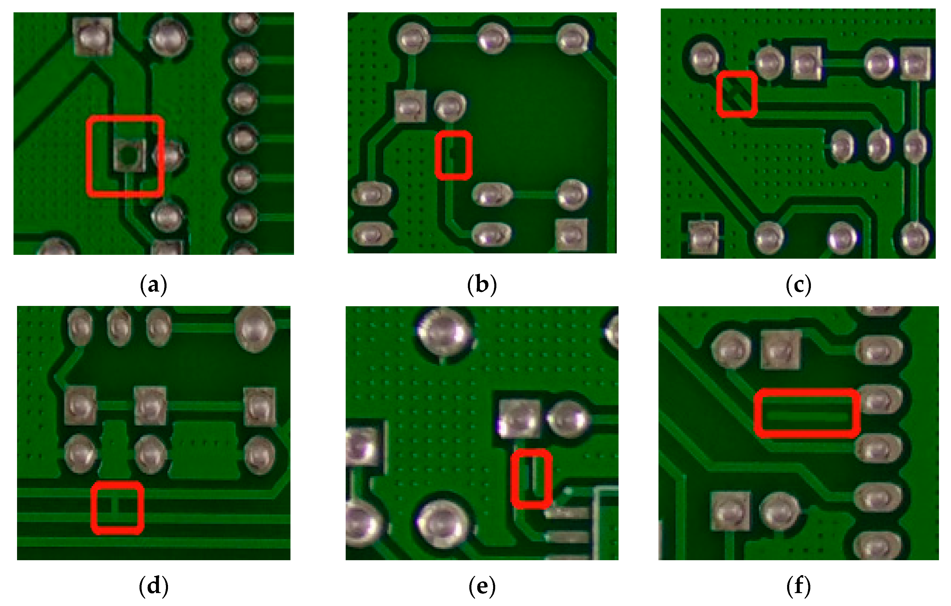
The experimental environment of this article is Ubuntu 20.04 LTS operating system, with an AMD Ryzen 7 5800H CPU and an NVIDIA GeForce RTX 3060 GPU. The acceleration library used is CUDA 11.7, and the PyTorch 1.13 framework is used.

3.2. Dataset

The open-source dataset from Peking University’s Intelligent Robot Open Laboratory was used for this study [55]. The entire dataset consists of 693 images, each with a size of 600 × 600 pixels, and contains 3–5 defects per image. The dataset encompasses six common defect types: missing hole, mouse bite, open circuit, short circuit, spur, and spurious copper, as illustrated in Figure 6.
The number of images for each type of defect in the PCB bare board image dataset and the corresponding counts of each defect type are shown in Table 1.
Due to the limited size of the dataset, which impacts the detection of PCB defects, data augmentation techniques were employed to enhance the generalization capability of the network prior to training. Data augmentation is a technique used to expand the training set by applying transformations such as rotation, cropping, and scaling to the original images, generating additional training data. This approach enhances the network’s ability to generalize. During network training, data augmentation is employed to augment the training dataset, thereby improving the network’s generalization capability. However, during network testing, the un-augmented test dataset is used to evaluate the network’s performance and generalization ability.
Using the aforementioned principles, this study initially divided the 693 original dataset images into training and testing sets in an 8:2 ratio. Data augmentation was exclusively applied to the training set, using common methods such as cropping, brightness adjustment, rotation, flipping, and scaling. Subsequently, all images were resized to a uniform dimension of 640 × 640. The augmented training set contains a total of 9920 images. The test set consists of 139 images, which are original images without undergoing any data augmentation operations.

3.3. Evaluation Indicators

Accuracy, Precision, Recall, and mean Average Precision (mAP) are evaluation metrics. Accuracy represents the proportion of correctly classified samples. Precision is the ratio of correctly classified attack samples to the total number of samples classified as attack samples. It is a measure of the classifier’s performance, generally higher values are better. Recall is the ratio of correctly classified attack samples to the actual number of attack samples and is used to evaluate the network’s detection capability for actual attacks. F 1 score is the harmonic mean of Precision and Recall, providing a balanced assessment of the network’s Precision and Recall performance. A higher F 1 score indicates a better balance between Precision and Recall. The specific formulas for calculation are as follows.
The ratio of correctly classified samples to the total number of samples is denoted as accuracy, A , calculated by the formula:
A = T P + T N T P + F N + F P + T N
The ratio of the number of true positive samples to the total number of samples is denoted as Precision, P, calculated by the formula:
P = T P T P + F P
The ratio between the number of detected true positive samples and the total number of true positive samples is denoted as Recall, R :
R = T P T P + F N
The harmonic mean of Precision and Recall is denoted as F 1 , and its calculation formula is as follows:
F 1 = 2 P r e c i s s i o n R e c a l l P r e c i s i o n + R e c a l l
where TP represents the number of samples correctly classified as attacks, FP represents the number of samples incorrectly classified as attacks, TN represents the number of samples correctly classified as normal, and FN represents the number of samples incorrectly classified as normal.
Using Precision or Recall alone cannot objectively reflect the quality of detection results. It is necessary to comprehensively evaluate algorithm performance by combining these two evaluation metrics. By using different combinations of Precision and Recall points, a Precision–Recall curve, or P-R curve, can be plotted. Based on the P-R curve, by calculating the Average Precision (AP) corresponding to each Recall value, the Average Precision can be obtained. The calculation formula is as follows:
A P = 0 1 P R d R
The sum of all AP values divided by the number of classes yields the mean Average Precision (mAP):
m A P = i = 0 n A P i n
[email protected]:.95 represents the mean Average Precision (mAP) calculated for IOU values ranging from 0.5 to 0.95 in increments of 0.05. It is the average of all mAP values calculated at different IOU thresholds.
To evaluate the accuracy of the proposed technique, three steps are undertaken:
(1)
Dataset Testing: experimental validation is conducted on publicly available PCB datasets to demonstrate the effectiveness of the PCBDD-DDNet method.
(2)
Performance Metrics: The primary performance metric used is mAP (mean Average Precision), with additional consideration of other metrics such as accuracy, Precision, and Recall. This comprehensive evaluation helps assess the overall performance of the method.
(3)
Comparison with Other Methods: comparative analysis is performed with existing classical deep learning methods to validate the accuracy of the proposed approach.

3.4. Experiment Results Analysis

3.4.1. Network Concatenation Performance Analysis

This experiment investigated the impact of network concatenation on network performance. The comparative experiment includes the CDBN network, the DenseNet network, and the D-DenseNet network where only these two networks are concatenated without any further modifications. The experiment evaluated the performance using Precision, Recall, and Average Precision Metrics. The experimental results are shown in Table 2.
The data from Table 2 indicates the following:
(1)
The D-DenseNet network obtained by concatenating the DBN network and the DenseNet network exhibited an improved detection performance.
(2)
The detection accuracy reached 91.43%, which is an increase of 4.86% compared to the CDBN network and a 0.61% improvement compared to the DenseNet network.
(3)
Moreover, the concatenated D-DenseNet network showed improvements of 1.51% in Recall rate and 3.98% in Average Precision compared to the CDBN network, and improvements of 0.73% in Recall rate and 0.75% in Average Precision compared to the DenseNet network.
(4)
The experiment demonstrated the enhanced performance of the D-DenseNet network achieved by concatenating the CDBN and DenseNet networks.

3.4.2. Performance Analysis of Multi-Scale Feature Extraction Network

This experiment investigated the impact of the multi-scale feature extraction network on network performance. The comparative experiment involved the original unmodified D-DenseNet network and the D-DenseNet network with an added multi-scale feature extraction module. The evaluation of this experiment was based on Precision, Recall, and Average Precision Metrics. The experimental results were presented in Table 3.
The data from Table 3 indicates the following:
(1)
Compared to the original, unimproved D-DenseNet network, the D-DenseNet network with the added multi-scale feature extraction module exhibited a better detection performance, achieving a detection accuracy of 91.90%, which was a 0.47% improvement over the original D-DenseNet network.
(2)
Furthermore, in terms of Recall and Average Precision, the D-DenseNet network with the multi-scale feature extraction module showed improvements of 1.19% and 1.04%, respectively, confirming the effectiveness of the multi-scale feature extraction module.

3.4.3. Performance Analysis of Adafactor Optimization Function and L2 Regularization

This experiment investigated the impact of the Adafactor optimization function and L2 regularization on network performance. Comparative experiments were conducted involving the original, unimproved D-DenseNet network, the D-DenseNet network with the added Adafactor optimization function, the D-DenseNet network with added L2 regularization, and the D-DenseNet network with both the Adafactor optimization function and L2 regularization. The evaluation was based on Precision, Recall, and Average Precision Metrics. The results of the experiment were presented in Table 4.
The data from Table 4 shows that:
(1)
Compared to the original unimproved D-DenseNet network, the D-DenseNet network with only the addition of the Adafactor optimization function had improved Precision by 0.24%, and the D-DenseNet network with only the addition of L2 regularization has improved the Precision by 0.29%.
(2)
The D-DenseNet network with both the Adafactor optimization function and L2 regularization showed better detection performance, achieving a Precision rate of 91.88%, which was a 0.45% improvement compared to the original unimproved D-DenseNet network.
(3)
Additionally, in terms of Recall and Average Precision, the D-DenseNet network with both the Adafactor optimization function and L2 regularization also outperformed the original unimproved network.
(4)
The experimental results demonstrated the effectiveness of the Adafactor optimization function and L2 regularization, as well as the continued improvement in network performance when both the Adafactor optimization function and L2 regularization are added simultaneously.

3.4.4. Performance Analysis of Hard Sample Mining Mechanism OHEM

This experiment investigated the impact of the hard sample mining mechanism OHEM on network performance. The comparative experiment involves the original unimproved D-DenseNet network and the D-DenseNet network with the introduction of the hard sample mining mechanism OHEM. The experiment evaluated the performance based on Precision, Recall, and Average Precision Metrics. The results of the experiment are shown in Table 5.
From the data in Table 5, the observations made are as follows:
(1)
Compared to the original unimproved D-DenseNet network, the D-DenseNet network with the introduction of the hard example mining mechanism (OHEM) exhibited a better detection performance.
(2)
The detection Precision rate reached 92.01%, which was an improvement of 0.58%. Additionally, there was an enhancement of 1.12% in Recall rate and 0.79% in Average Precision.
(3)
The experiment demonstrated that the OHEM mechanism for mining hard examples can enhance the network’s detection performance.

3.4.5. Comprehensive Analysis of Network Performance

This experiment conducted a comprehensive analysis of the impact of network concatenation, multi-scale feature extraction network, Adafactor optimization function, L2 regularization, and the OHEM mechanism on network performance. The evaluation was carried out using Precision, Recall, and Average Precision Metrics. The experimental results are presented in Table 6.
The data from Table 6 demonstrates the following:
(1)
Compared to the original D-DenseNet network without any improvements, the D-DenseNet networks enhanced with all the modifications in the text exhibited a better detection performance.
(2)
The detection accuracy reached 92.34%, showing an improvement of 0.91%. Additionally, the Recall rate and Average Precision reached 94.09% and 93.24%, respectively, showcasing improvements of 1.63% and 1.50% compared to the original D-DenseNet network.
(3)
These results validated the detection performance of the PCBDD-DDNet method.

3.4.6. Comparison of D-DenseNet Network with Other Classic Algorithms

To verify the performance of the network constructed in this chapter, we selected other deep learning detection methods at the same time: CDBN (Convolutional Deep Belief Network) [56], DenseNet (Dense Convolutional Network) [48], SSD512 (Single Shot MultiBox Detector512) [57], YOLOv3 (You Only Look Once version 3) [58], RetinaNet [59], Faster R-CNN (Faster Region Convolutional Neural Network), and FPN [60] for comparative experiments, with evaluations conducted for each respective set of evaluation metrics. The comparative experimental results for various networks were presented in Table 7.
The experimental results from Table 7 show the following:
(1)
The proposed D-DenseNet network in this paper outperformed other networks in terms of overall defect recognition performance, achieving higher evaluation metrics for Precision, Recall, and Average Precision.
(2)
Compared to using the CDBN network alone, the proposed network in this chapter achieved a 2.14% increase in Precision, a 5.77% increase in Recall, and a 4.78% increase in Average Precision.
(3)
Compared to using the DenseNet network alone, the proposed network in this chapter achieved a 1.36% increase in Precision, a 1.46% increase in Recall, and a 1.55% increase in Average Precision.
(4)
It can be seen that the proposed D-DenseNet achieved the highest detection accuracy, with a 93.24% mAP value, which is 4.79%, 3.96%, 2.60%, 1.58%, and 1.21% superior compared to RetinaNet, SSD, YOLOv3, RetinaNet, Faster-RCNN, and FPN, respectively. Meanwhile, D-DenseNet outperformed the other four compared models in P, R, and mAP.5:.95. Based on the comparison, the D-DenseNet model exhibited a significant advantage in terms of detection accuracy. Overall, the proposed network in this chapter demonstrates superior defect recognition capabilities.

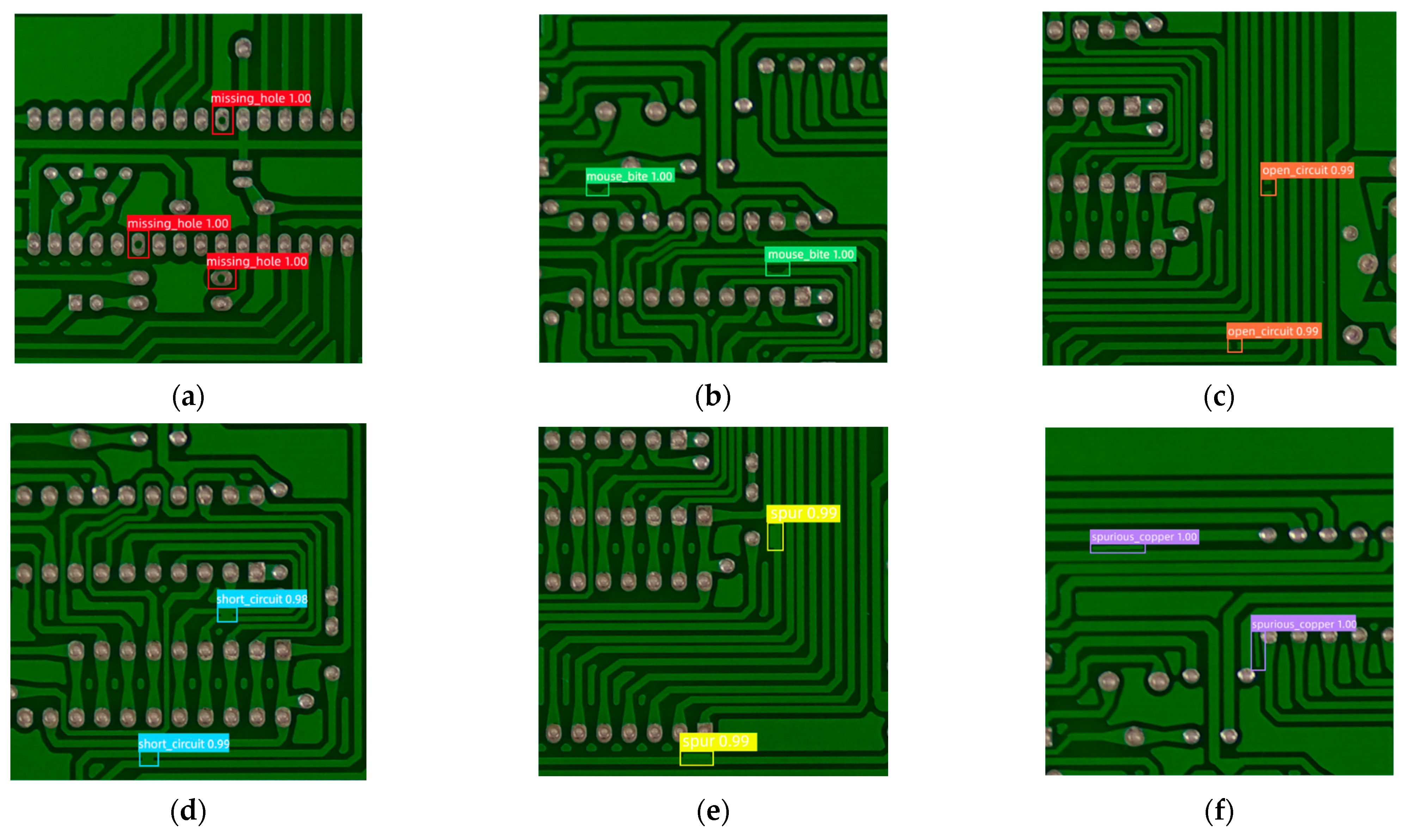
3.4.7. Display of Detection Effect

The proposed D-DenseNet network in this chapter is capable of accurately identifying the six types of defect categories on the PCB board. The specific detection results are shown in Figure 7. In the figure, the detection accuracy for missing hole, mouse bite, and spurious copper is 100%, while the accuracy for open circuit and spur is 99%, and the accuracy for short circuit is 99% for one class and 98% for another.

4. Conclusions

The proposed PCBDD-DDNet method exhibits significant advantages in PCB defect detection. Firstly, by constructing the D-DenseNet network, the strengths of two deep learning networks (CDBN and DenseNet) are fully leveraged. Specifically, CDBN is responsible for extracting low-level features, and DenseNet for high-level features, and their successful fusion through the concatenation layer further enhances network performance. Additionally, the introduced multi-scale feature extraction mechanism effectively captures information from different scales, enhancing feature representation. The integration of the Adafactor optimization function accelerates the convergence process, while L2 regularization effectively prevents overfitting. Finally, the use of the OHEM mechanism further improves the network’s ability to handle complex samples, thereby enhancing the accuracy of PCB defect detection.
The main novelties of this paper are reflected In three aspects. (1) Firstly, the construction of the D-DenseNet network is an innovative work that fully exploits the advantages of CDBN and DenseNet. Through reasonable connection and fusion, network performance is improved. (2) Secondly, the introduced multi-scale feature extraction mechanism enables the network to comprehensively capture image information, which is inspiring in the study of deep learning in the field of image processing. (3) Lastly, the integration of the Adafactor optimization function, L2 regularization, and the application of the OHEM mechanism provide effective means for the stability and generalization ability of the network, representing a beneficial attempt in the application of deep learning to PCB defect detection.
Through these advantages and novelties, the proposed method in this paper offers an advanced deep learning solution for PCB defect detection. Future research will aim to further refine this method to adapt to a wider range of scenarios and applications.

Author Contributions

Conceptualization, H.K. and Y.Y.; methodology, H.K.; software, Y.Y.; validation, H.K. and Y.Y.; formal analysis, H.K.; investigation, Y.Y.; resources, H.K.; data curation, Y.Y.; writing—original draft preparation, Y.Y.; writing—review and editing, H.K.; visualization, Y.Y.; supervision, H.K. All authors have read and agreed to the published version of the manuscript.

Funding

This research was funded by Humanities and Social Sciences research project of the Ministry of Education (grant number: 20YJAZH046) and the Scientific Research Project of the Beijing Educational Committee (grant number: KM202011232022).

Data Availability Statement

The data that support the findings of this study are available from the corresponding author upon reasonable request.

Acknowledgments

This study was supported by the Department of Information Security of Beijing Information Science and Technology University.

Conflicts of Interest

The authors declare no conflict of interest.

Abbreviations

AbbreviationsExplanations
X l output of layer l
H l nonlinear transformation function of layer l
K 0 initial number of channels
k growth rate per layer
lthe layer
v t moving average of the gradient square at the previous step
β 2 decay rate of the moving average
g t gradient at the current time step
αlearning rate
a small constant
γregularization parameter
w t parameter vector
w t + 1 updated parameter vector
λregularization coefficient
| w | 2 L2 norm
h ( x i ) model’s predicted value
y ( i ) actual value
L y i , y ( i ) the loss function used to measure the difference between the predicted and actual values
TPnumber of samples correctly classified as attacks
FPnumber of samples incorrectly classified as attacks
TNnumber of samples correctly classified as normal
FNnumber of samples incorrectly classified as normal
Aaccuracy
PPrecision
RRecall
F1the harmonic mean of Precision and Recall
APAverage Precision
mAPmean Average Precision

References

  1. Ling, Q.; Isa, N.A.M. Printed Circuit Board Defect Detection Methods Based on Image Processing, Machine Learning and Deep Learning: A Survey. IEEE Access 2023, 11, 15921–15944. [Google Scholar] [CrossRef]
  2. Chen, I.C.; Hwang, R.C.; Huang, H.C. PCB Defect Detection Based on Deep Learning Algorithm. Processes 2023, 11, 775. [Google Scholar] [CrossRef]
  3. Park, J.H.; Kim, Y.S.; Seo, H.; Cho, Y.J. Analysis of Training Deep Learning Models for PCB Defect Detection. Sensors 2023, 23, 2766. [Google Scholar] [CrossRef]
  4. Ren, Z.; Fang, F.; Yan, N.; Wu, Y. State of the art in defect detection based on machine vision. Int. J. Precis. Eng. Manuf.-Green Technol. 2022, 9, 661–691. [Google Scholar] [CrossRef]
  5. Aggarwal, N.; Deshwal, M.; Samant, P. A survey on automatic printed circuit board defect detection techniques. In Proceedings of the 2022 2nd International Conference on Advance Computing and Innovative Technologies in Engineering (ICACITE), Greater Noida, India, 28–29 April 2022; pp. 853–856. [Google Scholar]
  6. Griffin, P.M.; Villalobos, J.R.; Foster, J.W., III; Messimer, S.L. Automated visual inspection of bare printed circuit boards. Comput. Ind. Eng. 1990, 18, 505–509. [Google Scholar] [CrossRef]
  7. Putera, S.H.I.; Dzafaruddin, S.F.; Mohamad, M. MATLAB based defect detection and classification of printed circuit board. In Proceedings of the 2012 Second International Conference on Digital Information and Communication Technology and It’s Applications (DICTAP), Bangkok, Thailand, 16–18 May 2012; pp. 115–119. [Google Scholar]
  8. Li, Y.; Li, S. Defect detection of bare printed circuit boards based on gradient direction information entropy and uniform local binary patterns. Circuit World 2017, 43, 145–151. [Google Scholar] [CrossRef]
  9. Anoop, K.P.; Sarath, N.S.; Kumar, V.V. A review of PCB defect detection using image processing. Intern. J. Eng. Innov. Technol. 2015, 4, 188–192. [Google Scholar]
  10. Ren, J.; Gabbar, H.A.; Huang, X.; Saberironaghi, A. Defect Detection for Printed Circuit Board Assembly Using Deep Learning. In Proceedings of the 2022 8th International Conference on Control Science and Systems Engineering (ICCSSE), Guangzhou, China, 14–16 July 2022; pp. 85–89. [Google Scholar]
  11. Kuang, Y.; Ouyang, G.; Xie, H.; Hong, S.; Yang, J. Features learning method for PCB assembling defects inspection based on statistical analysis. Appl. Res. Comput. 2010, 27, 775–777+783. [Google Scholar]
  12. Gaidhane, V.H.; Hote, Y.V.; Singh, V. An efficient similarity measure approach for PCB surface defect detection. Pattern Anal. Appl. 2018, 21, 277–289. [Google Scholar] [CrossRef]
  13. Annaby, M.H.; Fouda, Y.M.; Rushdi, M.A. Improved normalized cross-correlation for defect detection in printed-circuit boards. IEEE Trans. Semicond. Manuf. 2019, 32, 199–211. [Google Scholar] [CrossRef]
  14. Tsai, D.M.; Huang, C.K. Defect detection in electronic surfaces using template-based Fourier image reconstruction. IEEE Trans. Compon. Packag. Manuf. Technol. 2018, 9, 163–172. [Google Scholar] [CrossRef]
  15. Cho, J.W.; Seo, Y.C.; Jung, S.H.; Jung, H.K.; Kim, S.H. A study on real-time defect detection using ultrasound excited thermography. J. Korean Soc. Nondestruct. Test. 2006, 26, 211–219. [Google Scholar]
  16. Wu, X.; Ge, Y.; Zhang, Q.; Zhang, D. PCB defect detection using deep learning methods. In Proceedings of the 2021 IEEE 24th International Conference on Computer Supported Cooperative Work in Design (CSCWD), Dalian, China, 5–7 May 2021; pp. 873–876. [Google Scholar]
  17. Raffik, R.; Sabitha, B.; Arunprasanth, D.; Karthikeyan, E.; Padmanaaban, A.G.; Prasanth, V.S. Automated PCB Defect Identification System using Machine Learning Techniques. In Proceedings of the 2023 2nd International Conference on Advancements in Electrical, Electronics, Communication, Computing and Automation (ICAECA), Tianjin, China, 4–7 August 2023; pp. 1–5. [Google Scholar]
  18. Hu, Y.; Tan, Y. State and Development of Automatic Optical Inspection Applications in China. Microcomput. Inf. 2006, 22, 143–146. [Google Scholar]
  19. Zakaria, S.S.; Amir, A.; Yaakob, N.; Nazemi, S. Automated detection of printed circuit boards (PCB) defects by using machine learning in electronic manufacturing: Current approaches. In Iop Conference Series: Materials Science and Engineering; IOP Publishing: Bristol, UK, 2020; Volume 767, p. 012064. [Google Scholar]
  20. Pal, A.; Chauhan, S.; Bhardwaj, S.C. Detection of bare PCB defects by image subtraction method using machine vision. Lect. Notes Eng. Comput. Sci. 2011, 2191, 1597–1601. [Google Scholar]
  21. Malge, P.S.; Nadaf, R.S. PCB defect detection, classification and localization using mathematical morphology and image processing tools. Int. J. Comput. Appl. 2014, 87, 40–45. [Google Scholar]
  22. Ray, S.; Mukherjee, J. A hybrid approach for detection and classification of the defects on printed circuit board. Int. J. Comput. Appl. 2015, 121, 42–48. [Google Scholar] [CrossRef]
  23. Dave, N.; Tambade, V.; Pandhare, B.; Saurav, S. PCB defect detection using image processing and embedded system. Int. Res. J. Eng. Technol. 2016, 3, 1897–1901. [Google Scholar]
  24. Huang, Z.; Pan, Z.; Lei, B. Transfer learning with deep convolutional neural network for SAR target classification with limited labeled data. Remote Sens. 2017, 9, 907. [Google Scholar] [CrossRef]
  25. Zhuang, N.; Yan, Y.; Chen, S.; Wang, H.; Shen, C. Multi-label learning based deep transfer neural network for facial attribute classification. Pattern Recognit. 2018, 8, 225–240. [Google Scholar] [CrossRef]
  26. Chen, X.; Yu, J.D.; Chen, X.A. Classification of Electronic Components Based on Convolution Neural Network. Wirel. Commun. Technol. 2018, 2, 7–12. [Google Scholar]
  27. Wang, Y.L.; Cao, J.T.; Ji, X.F. PCB defect detection and recognition algorithm based on convolutional neural network. J. Electron. Meas. Instrum. 2019, 33, 78–84. [Google Scholar]
  28. Hu, B.; Wang, J. Detection of PCB Surface Defects with Improved Faster-RCNN and Feature Pyramid Network. IEEE Access 2020, 8, 108335–108345. [Google Scholar] [CrossRef]
  29. Chen, W.S.; Ren, Z.G.; Wu, Z.Z. Detecting Object and Direction for Polar Electronic Components via Deep Learning. Acta Autom. Sin. 2021, 47, 1701–1709. [Google Scholar]
  30. Wu, J.G.; Cheng, Y.; Shao, J.; Yang, D. A defect detection method for PCB based on the improved YOLOv4. Chin. J. Sci. Instrum. 2021, 38, 912–917. [Google Scholar]
  31. Hu, S.S.; Xiao, Y.; Wang, B.S.; Yin, J.Y. Research on PCB defect detection based on deep learning. Electr. Meas. Instrum. 2021, 58, 139–145. [Google Scholar]
  32. Zhang, L.; Shen, J.; Zhang, J.; Xu, J.; Li, Z.; Yao, Y.; Yu, L. Multimodal marketing intent analysis for effective targeted advertising. IEEE Trans. Multimed. 2021, 24, 1830–1843. [Google Scholar] [CrossRef]
  33. Liu, Z.; Wang, Q.; Nestler, R.; Notni, G. Investigation on automated visual SMD-PCB inspection based on multimodal one-class novelty detection. In Multimodal Sensing and Artificial Intelligence: Technologies and Applications III; SPIE: Philadelphia, PA, USA, 2023; Volume 12621, pp. 246–256. [Google Scholar]
  34. Lu, Z.; He, Q.; Xiang, X.; Liu, H. Defect detection of PCB based on Bayes feature fusion. J. Eng. 2018, 2018, 1741–1745. [Google Scholar] [CrossRef]
  35. Shen, J.; Robertson, N. BBAS: Towards large scale effective ensemble adversarial attacks against deep neural network learning. Inf. Sci. 2021, 569, 469–478. [Google Scholar] [CrossRef]
  36. Shi, W.; Zhang, L.; Li, Y.; Liu, H. Adversarial semi-supervised learning method for printed circuit board unknown defect detection. J. Eng. 2020, 2020, 505–510. [Google Scholar] [CrossRef]
  37. You, S. PCB defect detection based on generative adversarial network. In Proceedings of the 2022 2nd International Conference on Consumer Electronics and Computer Engineering (ICCECE), Guangzhou, China, 14–16 January 2022; pp. 557–560. [Google Scholar]
  38. Yang, B.; Nie, Y.; Cui, W.; Sun, J.; Lu, H.; Su, W. Generative adversarial network for PCB defect detection with extreme low compress rate. In Proceedings of the International Conference on Artificial Intelligence and Intelligent Information Processing (AIIIP 2022), Hangzhou, China, 24–25 November 2022; Volume 12456, pp. 331–337. [Google Scholar]
  39. Yan, C.; Gong, B.; Wei, Y.; Gao, Y. Deep multi-view enhancement hashing for image retrieval. IEEE Trans. Pattern Anal. Mach. Intell. 2020, 43, 1445–1451. [Google Scholar] [CrossRef]
  40. Longjiang, Y.; Ying, Y.; Shenghe, S. A PCB Component Location Method Based on Image Hashing. In Proceedings of the 2007 8th International Conference on Electronic Measurement and Instruments, Xi’an, China, 16–18 August 2007; pp. 2-697–2-700. [Google Scholar]
  41. Moganti, M.; Ercal, F.; Dagli, C.H.; Tsunekawa, S. Automatic PCB inspection algorithms: A survey. Comput. Vis. Image Underst. 1996, 63, 287–313. [Google Scholar] [CrossRef]
  42. Chen, S.C. Multimedia deep learning. IEEE MultiMedia 2019, 26, 5–7. [Google Scholar] [CrossRef]
  43. Jeon, G.; Anisetti, M.; Damiani, E.; Kantarci, B. Artificial intelligence in deep learning algorithms for multimedia analysis. Multimed. Tools Appl. 2020, 79, 34129–34139. [Google Scholar] [CrossRef]
  44. Ota, K.; Dao, M.S.; Mezaris, V.; Natale, F.G.D. Deep learning for mobile multimedia: A survey. ACM Trans. Multimed. Comput. Commun. Appl. (TOMM) 2017, 13, 1–22. [Google Scholar] [CrossRef]
  45. Zhang, W.; Yao, T.; Zhu, S.; Saddik, A.E. Deep learning–based multimedia analytics: A review. ACM Trans. Multimed. Comput. Commun. Appl. (TOMM) 2019, 15, 1–26. [Google Scholar] [CrossRef]
  46. Yuan, X.; Rao, J.; Gu, Y.; Ye, L.; Wang, K.; Wang, Y. Online adaptive networking framework for deep belief network-based quality prediction in industrial processes. Ind. Eng. Chem. Res. 2021, 60, 15208–15218. [Google Scholar] [CrossRef]
  47. Zhang, N.; Ding, S.; Zhang, J.; Xue, Y. An overview on restricted Boltzmann machines. Neurocomputing 2018, 275, 1186–1199. [Google Scholar] [CrossRef]
  48. Huang, G.; Liu, Z.; Van Der Maaten, L.; Weinberger, K.Q. Densely connected convolutional networks. In Proceedings of the IEEE Conference on Computer Vision and Pattern Recognition, Honolulu, HI, USA, 21–26 July 2017; pp. 4700–4708. [Google Scholar]
  49. Hu, W.; Wang, T.; Wang, Y.; Chen, Z.; Huang, G. LE–MSFE–DDNet: A defect detection network based on low-light enhancement and multi-scale feature extraction. Vis. Comput. 2022, 38, 3731–3745. [Google Scholar] [CrossRef]
  50. Kang, H.; Ji, Y.; Zhang, S. Enhanced Privacy Preserving for Social Networks Relational Data Based on Personalized Differential Privacy. Chin. J. Electron. 2022, 31, 741–751. [Google Scholar] [CrossRef]
  51. Wang, L.; Meng, Z.Q.; Yang, L.N. Chinese Sentiment Analysis Based on CNN-BiLSTM Model of Multi-level and Multi-scale Feature Extraction. Comput. Sci. 2023, 50, 248–254. [Google Scholar]
  52. Shazeer, N.; Stern, M. Adafactor: Adaptive learning rates with sublinear memory cost. In Proceedings of the International Conference on Machine Learning, Stockholm, Sweden, 10–15 July 2018; pp. 4596–4604. [Google Scholar]
  53. Shi, G.; Zhang, J.; Li, H.; Wang, C. Enhance the performance of deep neural networks via L2 regularization on the input of activations. Neural Process. Lett. 2019, 50, 57–75. [Google Scholar] [CrossRef]
  54. Shi, F.; Qian, H.; Chen, W.; Huang, M.; Wan, Z. A fire monitoring and alarm system based on YOLOv3 with OHEM. In Proceedings of the 2020 39th Chinese Control Conference (CCC), Shenyang, China, 27–29 July 2020; pp. 7322–7327. [Google Scholar]
  55. Ding, R.; Dai, L.; Li, G.; Liu, H. TDD-net: A tiny defect detection network for printed circuit boards. CAAI Trans. Intell. Technol. 2019, 4, 110–116. [Google Scholar] [CrossRef]
  56. Shao, H.; Jiang, H.; Zhang, H.; Liang, T. Electric locomotive bearing fault diagnosis using a novel convolutional deep belief network. IEEE Trans. Ind. Electron. 2017, 65, 2727–2736. [Google Scholar] [CrossRef]
  57. Kang, L.; Ge, Y.; Huang, H.; Zhao, M. Research on PCB defect detection based on SSD. In Proceedings of the 2022 IEEE 4th International Conference on Civil Aviation Safety and Information Technology (ICCASIT), Dali, China, 12–14 October 2022; pp. 1315–1319. [Google Scholar]
  58. Lan, Z.; Hong, Y.; Li, Y. An improved YOLOv3 method for PCB surface defect detection. In Proceedings of the 2021 IEEE International Conference on Power Electronics, Computer Applications (ICPECA), Shenyang, China, 22–24 January 2021; pp. 1009–1015. [Google Scholar]
  59. Cheng, X.; Yu, J. RetinaNet with difference channel attention and adaptively spatial feature fusion for steel surface defect detection. IEEE Trans. Instrum. Meas. 2020, 70, 1–11. [Google Scholar] [CrossRef]
  60. Lin, T.Y.; Dollar, P.; Girshick, R.; He, K.; Hariharan, B.; Belongie, S. Feature pyramid networks for object detection. In Proceedings of the Computer Vision and Pattern Recognition (CVPR), Honolulu, HI, USA, 21–26 July 2017; pp. 936–944. [Google Scholar]
Figure 1. Overall flowchart of PCBDD-DDNet.
Electronics 12 04737 g001
Figure 2. Diagram of the D-DenseNet network architecture.
Electronics 12 04737 g002
Figure 3. Network integration.
Electronics 12 04737 g003
Figure 4. Feature vector concatenation.
Electronics 12 04737 g004
Figure 5. Multi-scale model network structure diagram.
Electronics 12 04737 g005
Figure 6. Diagram of 6 defect types: (a) missing hole; (b) mouse bite; (c) open circuit; (d) short circuit; (e) spur; and (f) spurious copper.
Electronics 12 04737 g006
Figure 7. Sample test results: (a) missing hole; (b) mouse bite; (c) open circuit; (d) short circuit; (e) spur; and (f) spurious copper.
Electronics 12 04737 g007
Table 1. The quantity of images in the PCB dataset and the count of each defect type.
Defect TypeMissing HoleMouse BiteOpen CircuitShort
Circuit
SpurSpurious Copper
Number of pictures116115116116115115
Number of defects503497482491488492
Table 2. Network concatenation performance comparison.
ExperimentP/%R/%mAP/%mAP.5:.95/%
DBN86.5790.9587.7649.56
DenseNet90.8291.7390.9950.13
D-DenseNet network with concatenation only and no further improvements91.4392.4691.7450.29
Table 3. Performance comparison with and without multi-scale feature extraction module.
ExperimentP/%R/%mAP/%mAP.5:.95/%
Original, unimproved D-DenseNet network91.4392.4691.7450.29
D-DenseNet network with added multi-scale feature extraction module91.9093.6592.7850.35
Table 4. Comparison of Adafactor Optimization Function and L2 Regularization Performance.
ExperimentP/%R/%mAP/%mAP.5:.95/%
D-DenseNet network with concatenation only and no further improvements91.4392.4691.7450.29
Only adding the Adafactor optimization function91.6792.7392.1850.31
Only adding L2 regularization91.7292.8792.2450.32
Simultaneously adding the Adafactor optimization function and L2 regularization91.8893.1592.3350.33
Table 5. Performance analysis of Hard Sample Mining Mechanism, OHEM.
ExperimentP/%R/%mAP/%mAP.5:.95/%
D-DenseNet network with concatenation only and no further improvements91.4392.4691.7450.29
D-DenseNet network with the introduction of OHEM92.0193.5892.5350.34
Table 6. Comprehensive analysis of network performance.
ExperimentP/%R/%mAP/%mAP.5:.95/%
D-DenseNet network with concatenation only and no further improvements91.4392.4691.7450.29
Adding Multi-Scale Feature Extraction Module91.9093.6592.7850.35
Adding Only Adafactor Optimization Function91.6792.7392.1850.31
Adding Only L2 Regularization91.7292.8792.2450.32
Introducing Hard Example Mining Mechanism (OHEM)92.0193.5892.5350.34
PCBDD-DDNet92.3494.0993.2450.48
Table 7. Comparison of results from various networks.
ExperimentP/%R/%mAP/%mAP.5:.95/%
CDBN86.5790.9587.7649.56
DenseNet90.8291.7390.9950.13
SSD51285.3688.7988.4548.07
YOLOv387.2089.1689.2849.58
RetinaNet89.9191.8790.6449.77
Faster R-CNN91.6792.4891.6650.21
FPN91.8192.9792.0350.27
D-DenseNet92.3494.0993.2450.48
Disclaimer/Publisher’s Note: The statements, opinions and data contained in all publications are solely those of the individual author(s) and contributor(s) and not of MDPI and/or the editor(s). MDPI and/or the editor(s) disclaim responsibility for any injury to people or property resulting from any ideas, methods, instructions or products referred to in the content.

