1. Introduction
Renewable energy has gained recent attention due to concerns regarding climate change and the unavoidable reduction of non-renewable energy resources. The need for efficient and sustainable energy conversion systems has become paramount. Renewable energy sources such as solar, wind, and hydroelectric power have emerged as viable alternatives to traditional fossil fuels [
1,
2,
3,
4].
A crucial component in integrating and optimizing these energy conversion systems is the efficient conversion and management of the generated electrical power. In this context, DC–DC converters have emerged as essential power electronics devices, providing the means to adapt and condition the generated power to suit the specific requirements of various applications [
5,
6,
7].
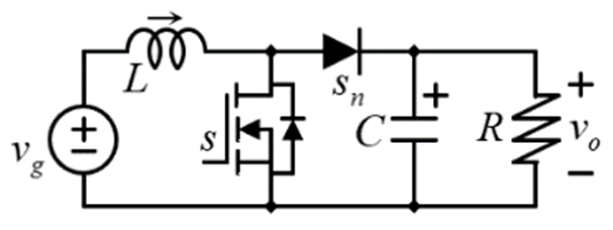
Figure 1 shows the traditional boost converter, a widely used topology [
5,
6], characterized by producing an output voltage larger than its input voltage, whose output can be regulated with the transistor’s duty cycle. Moreover, its input current is continuous (non-pulsating), which represents an advantage. Its main disadvantage is that with duty cycles close to one, both the efficiency and real voltage gain decrease [
5,
6]. This limitation is caused by parasitic components, particularly the DC resistance of the inductor and the on-resistance of the transistor.
To avoid the described effect, it is common in practice to impose limitations in commercial converters, typically around 0.75 to 0.8 for the duty cycle [
6] or around 4 to 5 in the voltage gain. If the voltage gain has to be larger than five, then the boost converter by itself may not be an adequate solution. Still, large-voltage-gain conversions are performed, and the research on high-voltage-gain converters is an active field of research.
A feasible DC–DC topology solution to generate a large voltage gain consists of the cascade connection of two boost converters (the second converter’s input is the first converter’s output). In recent works, some DC–DC converters producing large voltage gains have been proposed, for instance, converters with input-parallel output-series connections, cascaded converters, and converters that are based on voltage lift techniques, among others [
7,
8,
9,
10].
A desirable feature of a DC–DC converter is to have a compact inductor. The size of the inductance is related to two main factors: its inductance and its maximum current. This considers inductors made in cores with the same material and maximum flux density.
Figure 2 shows an inductor made with a toroidal core. We must define a maximum flux density we can allow, knowing that the inductance would decrease as the flux density increases. This would result in a maximum current through the core of the window or a maximum current through the winding (related to the total current and the number of turns). The maximum flux density is defined considering the core saturation.
The maximum stored energy in an inductor can be expressed as (1):
with
L being the inductance, and
iL, the current. The inductance can be expressed as (2):
where
N is the number of turns in the winding, and
is the reluctance, in this case, the reluctance must be calculated at the maximum allowed value of flux density. We can increase the number of turns to increase the inductance, but this would reduce the maximum current through the wire, which can be defined as (3):
If we increase the number of turns, we get an inductor with more inductance but less maximum current, and vice versa. It seems the core does not provide a particular parameter to the inductor, but it does. We can calculate the maximum stored energy in the inductor by considering the maximum current and by substituting (2) and (3) in (1), which results in (4):
The maximum stored energy is directly related to the core. If we achieve a design of a converter whose inductor requires a smaller amount of stored energy, this would result in a smaller core. We can bring some directions by knowing the relationship between the stored energy, the current, and the inductance of an inductor. Most boost-type converters have an inductor in series with the input source, and the input current is the largest current in most boost-type converters. Furthermore, the inductance of the inductor defines the maximum Input current ripple, which is an important design constraint.
This article introduces a step-up DC–DC converter topology with a larger relation of duty cycle vs. voltage gain compared to the traditional boost converter topology. The proposed topology benefits from a low inductor current (lower than the current at the input port) while maintaining the non-pulsating characteristic of the input current. This topology is referred to in what follows as the Reduced Inductor Current Multilevel Boost Converter (RIC-MBC) and was initially introduced in [
11] with preliminary results. The proposed RIC-MBC topology is similar (but not equal) to the Multilevel Boost Converter (MBC), which has been the subject of several studies leading to new families of topologies that can be sorted into converters with only one inductor [
12,
13,
14,
15,
16] and interleaved or converters with more than one inductor [
17,
18,
19,
20]. Some converter families have been proposed based on the MBC principle [
21]; their mathematical modeling has also been investigated [
22,
23].
The RIC-MBC also requires a smaller inductance (compared to the classical boost converter) to achieve the same input current ripple. The reduction in the inductance and the current with the proposed RIC-MBC topology results in a reduction in the stored energy in the inductor (lower inductance and lower current), compared to the classical boost converters. The proposed topology can be scaled up to obtain a full family of large-voltage-gain converters. A family of converters with the additional benefit of requiring fewer components than the Multilevel Boost Converter for the same number of output levels. In this paper, we present the mathematical model, simulation, and experiments to assess the benefits of the proposition.
After the introduction provided in
Section 1,
Section 2 introduces the proposed topology;
Section 3 discusses the selection of components;
Section 4 introduces a comparison with other topologies, in this case, the traditional boost converter and the multilevel boost converter;
Section 5 discusses how the proposed converter can be extended to a family of converters;
Section 6 presents experimental results; Finally,
Section 7 presents the conclusions and future works.
2. Proposed Topology
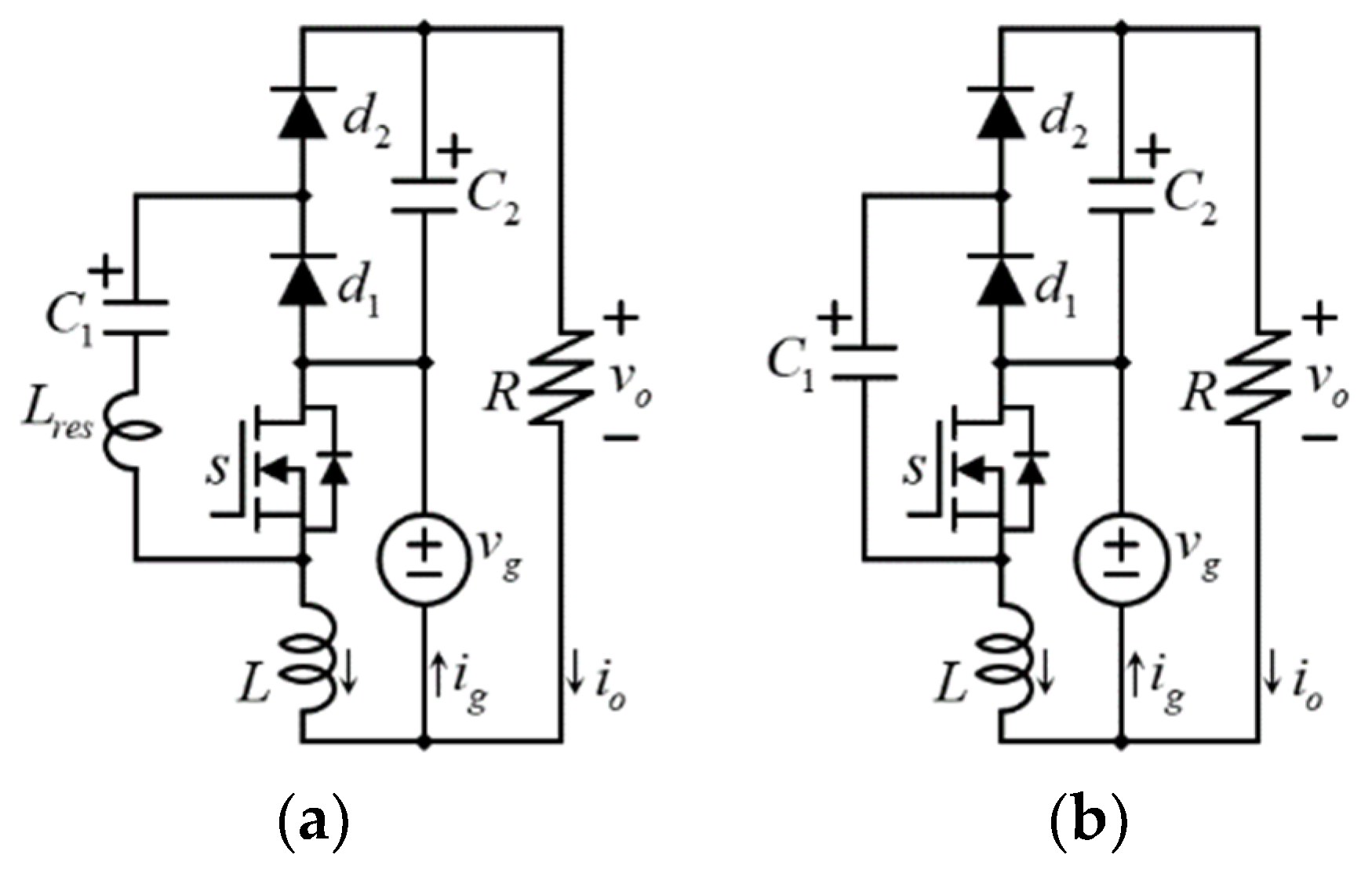
Figure 3 shows a basic case of the proposed RIC-MBC topology corresponding to the 3-level case that will be used as a starting point for analysis to easily understand the idea behind it. In
Section 5, this basic topology is later extended to consider more levels. The level count indicates the number of voltage levels observed at the output port, including the ground reference; hence, the classical boost converter (
Figure 1) would be a topology of two levels. Notice that, in contrast to many boost-type converters, the inductor shares the ground node with the load and the input voltage source, and it is not series connected with the input. If the inductor is in series with the input voltage source, the inductor current would be the same as the input current; in a boost converter, the input current is usually the largest current, and the output current is usually the smallest one. The impact of the ground connection can be seen by applying the KCL to the ground node (see
Figure 3). Since the inductor and the load current are in the same direction, they both together make the input current, and then, the inductor current is always smaller than the input current.
Figure 3a shows the complete proposed topology, including a small resonant inductor in series with
C1. This inductor may be omitted, depending on the application. To facilitate the analysis, the presentation focuses on the topology of
Figure 3b, where the resonant inductor has been omitted.
Figure 4 shows the equivalent circuits of the proposed 3-level topology for the corresponding switching state and considering continuous conduction mode (CCM) operation.
Figure 4a shows the circuit when the transistor is closed (diode open), while
Figure 4b shows the circuit when the transistor is open.
Basically, when the switch is closed, the inductor current rises (getting charged). Now, when the switch is open, the inductor charges (transfers current to) the capacitor C1. If the transistor is closed, then diode d1 remains open since the voltage across C1 inversely polarizes it. If the transistor opens, then the current through L forces the closing of diode d1. The capacitor C2 gets charged as it gets in parallel connection to C1 once the switch closes. Notice that d2 remains open when d1 is closed since d2 is reverse-biased by the capacitor C2.
The equivalent circuits depicted in
Figure 4 and the conventional averaging technique [
5] allow us to represent the dynamics of the inductor current through Equation (5):
where “
L” is the inductance of the inductor,
iL is the inductor current,
d is the transistor’s duty cycle,
vg is the voltage at the input port, and
vC1 is the voltage across the terminals of capacitor
C1. The first expression at the right side
d(vg) is the duty cycle
d = ton/TS multiplied by the voltage across the inductor when the switch is closed. The second expression of the right side (1 −
d)(
vg −
vC1) is the complement of the duty cycle multiplied by the voltage across the inductor when the switch is off.
In Equation (5), see
Figure 4a, if the switch is closed, the voltage of the inductor equals
vg, which brings the first term on the right-hand side (RHS) of (5). On the other hand, if the switch is open, the voltage across the inductor is
vg −
vC1 (see
Figure 4b), which brings the second term to the RHS of (5).
From (5), the equilibrium of the voltage in
C1 can be obtained by zeroing the derivative, and considering the small ripple approximation [
5],
VC1 can be written as (6):
where uppercase letters denote steady-state or direct current (DC) values.
If the transistor closes (see
Figure 4a), then capacitor
C1 gets in parallel with
C2; consequently, both capacitors get the same voltage, i.e., the capacitor’s voltages get balanced as in a switched capacitors converter.
Both diodes, as indicated by Equation (7), are rated for the same voltage and, on average, conduct the output current. This can be inferred by examining
Figure 3 and considering that the direct current output cannot pass through the capacitors.
The output voltage of the proposed converter is obtained by adding the input voltage
vg to the voltage
vC2. Hence, Equation (8) gives the output voltage of the suggested converter:
It is important to note that while the voltage of the capacitor, as represented by Equations (6) and (7), has the same mathematical expression as in the classical boost topology, the gain is larger in the RIC-MBC. In consequence, the duty cycle is smaller for the same operating conditions, and capacitors sustain a relatively smaller voltage compared to the one in the classical boost topology.
The current at the output port can be represented as indicated in Equation (9):
where
R is the output (or load) resistance (see
Figure 3).
3. Selection of Components
This section discusses the selection of the converter components. It covers the inductance calculation to match a desired input current, the capacitance calculation to match a desired output voltage ripple, and the calculation of the losses in components.
Application of the KCL to the bottom node in
Figure 3 yields:
i.e., the current flowing through the inductor is equivalent to the difference between the input and output currents. This represents an advantage with respect to the traditional boost where the inductor current equals the input current; that is, a reduction in the current for the same operating condition is an advantage.
From
Figure 4a, the inductance can be determined as follows:
where Δ
iL is the current ripple through the inductor,
D is the duty cycle, and
TS is the switching period (inverse of the switching frequency). The number two comes from the standard definition indicating that when the switch is closed, the total change in the inductor current is equivalent to twice the current ripple since the current ripple is defined as the maximum deviation from the average current
IL.
From
Figure 3, we can also say that if the capacitors are chosen in a way to have a small ripple (small ripple approximation), then the output current would have a small ripple, and the input current ripple will be equal to the inductor current ripple. The inductor can be selected to attain a desired input current ripple with (11). Notice that (11) also has the same mathematical expression as in the classical boost topology; however, notice that the inductor is proportional to the duty cycle, and then, the large voltage gain obtained with a relatively small duty cycle results in a small inductance. This explains why, for the same operating condition, the proposed converter requires a smaller inductance value to provide the same input current ripple.
Section 4 presents a comparative evaluation between the proposed converter and the traditional boost converter, where this fact is noted.
Two important parameters to consider while selecting the inductor are the RMS current and the peak current. The RMS current can be calculated as follows (from [
5] Appendix 1, page 806):
where
IL-RMS is the RMS value of the current through the inductor, and
IL is the average current. The peak current through the inductor is given by:
Both capacitors achieve the DC voltage expressed in (6). As mentioned above, due to the larger voltage gain achieved with the proposed converter as compared to the traditional boost converter, the required duty cycle for a particular gain is smaller, and thus, the capacitors in the proposed converter are rated to a smaller voltage as compared to the traditional boost.
From
Figure 4b, the voltage ripple of capacitor
C2 is given by (14):
where Δ
vC2 is the voltage ripple in the capacitor
C2,
Io is the output current as defined in (9),
D is the duty cycle, and
TS is the switching period (inverse of the switching frequency). Similar to (11), the number two comes from the standard definition, indicating that when the switch is open, the total change in the capacitor voltage is equivalent to twice the voltage ripple since the voltage ripple is defined as the maximum deviation from the average voltage
VC2.
Note from (14) and
Figure 4 that capacitor
C2 discharges during the full switching cycle and gets charged only for a short time when the switch closes. During the steady state operation, the charge the capacitor obtains must be equal to the total charge it provides to the load, and thus, the voltage ripple can be calculated as in (14).
Figure 3 reveals that the output voltage ripple, produced by the converter switching action, is equal to the voltage ripple on capacitor
C2. Let us consider in this article, for the sake of simplicity, that both capacitors have the same capacitance, i.e.,
C1 =
C2 =
C; therefore, capacitor
C2 can be selected to attain the desired output voltage ripple as follows:
Before dealing with the capacitor
C1, let us define the total charge provided by
C2 to the load (only) when the switch is off as follows:
This term explicitly appears in (15); that is, C2 is calculated to have a particular voltage ripple while providing this charge.
Now, when the switch is closed (see
Figure 4a), the capacitor
C1 transfers this charge to
C2, and both (
C1 and
C2) provide the load current during the on-time
DTS.
The total charge provided by
C1 during the time in which the switch is closed is given by:
If the capacitors are equal (
C1 =
C2 =
C), then (17) can be rewritten as:
Therefore, if a particular voltage ripple is desired in
C1, then, from (16)–(18), it can be chosen as:
The switching transistor (see
Figure 3) must be rated to the voltage in
C1 (described in (6) and (7)) since this is the voltage to be blocked when the transistor is open (see
Figure 4b). Its current can be approximated as a pulsating waveform with a linear ripple plus the charge interchanged by the capacitors. The following expression provides an approximation to this current (based on [
5] Appendix 1, page 807):
Factor
β is around 1 if resonant charge interchange is used. Otherwise, it can be approximated if one knows the percentage of
TS, which can be called
DQ, in which the charge is interchanged.
All diodes are rated to the same voltage described in (6). The most relevant current for the diodes is their average current, in this case, the load current Io, since their conduction losses can be calculated with acceptable precision as the product of their on-voltage multiplied by their average current.
4. Comparison with Other Topologies
As mentioned above, the reduction of the current in the proposed topology leads to a lower stored energy in the inductor while maintaining continuity in the input current and the same input current ripple. To understand the advantages of the proposed topology, this section provides a comparison evaluation, firstly against the well-known and widely used traditional boost converter and then against the conventional MBC.
The comparison study consists of designing converters for the same output voltage specification and then comparing the converters in terms of the stored energy in inductors. For this, consider that the converters must boost an input voltage fluctuating between 36 V and 50 V to an output regulated to 200 V.
The 200 V output is suitable to potentially power a 120 V H-bridge inverter, among other things. Let us consider that the output power is 200 W and the switching frequency is fS = 100 kHz. Furthermore, as a design specification, the converter is required to function with a normalized input current ripple of 15%. The normalized input current ripple will be calculated by dividing the input current ripple over the input DC current.
The purpose of the comparison is that it can be easily reproduced in a circuit simulator. In this case, the simulator may reproduce the following operation point, i.e., an input voltage of vg = 50 V, an output voltage of vo = 200 V, and a load resistance of R = 200 Ω.
4.1. Comparison vs. the Traditional Boost Converter
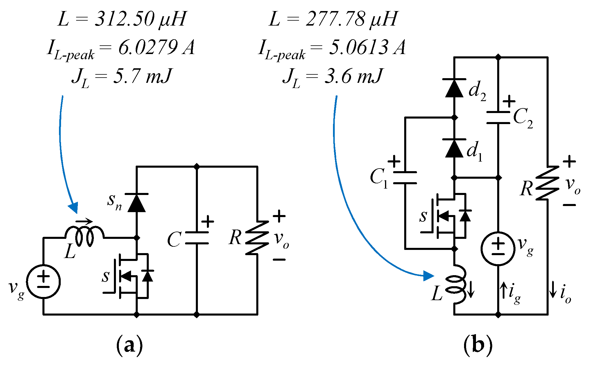
As mentioned before, each converter would require different parameters (inductance and duty cycle) to comply with the same specifications gain and input current ripple. The traditional boost converter requires an inductance of 312.50 μH. Furthermore, the boost converter drains a maximum peak current of 6.0279 A. This solution is shown in
Figure 5. The proposed RIC-MBC requires an inductor of 277.78 μH and drains a peak current of 5.06 A. These inductances are the minimum required on each topology to achieve the specified input current ripple. As observed, the proposed converter requires less inductance, and its inductor drains a smaller current. Moreover, the stored energy in the proposed converter is about 63% of that of the traditional boost converter (see
Figure 5).
Furthermore, the semiconductors and capacitors of the proposed RIC-MBC are rated to 164 V, in contrast with the traditional boost converter, where devices are rated to the output voltage of 200 V.
The comparison verifies the advantage of the proposed RIC-MBC compared to the classic boost topology. The inductor of the RIC-MBC has smaller inductance, current, and stored energy, which is about 63% of the stored energy of the traditional boost converter, which is an important feature as it is related to the size of the core.
Similar to the traditional boost converter, the RIC-MBC can be configured in an interleaving configuration while maintaining its superior characteristics.
The traditional boost converter requires a capacitor of 41 μF to achieve a 0.2 V peak-to-peak output voltage ripple, while the proposed RIC-MBC converter requires capacitors of 30 μF. In the case of capacitors having different capacitance and voltage, it results that the same stored energy in capacitors is required in both converters, 820 mJ. This means that there is no difference on the capacitor’s side. However, the proposed RIC-MBC converter requires an extra diode, which represents a disadvantage. Furthermore, the topology in
Figure 3b has a non-resonant charge interchange among capacitors [
10]. Therefore, the peak current among them is limited only by the parasitic resistance on the charging path. This can be solved by adding a relatively small resonant inductor. For medium or high-power converters, the inductance associated with the wire path is enough, as previously reported for other switched capacitor circuits [
10,
15].
4.2. Comparison vs. the MBC
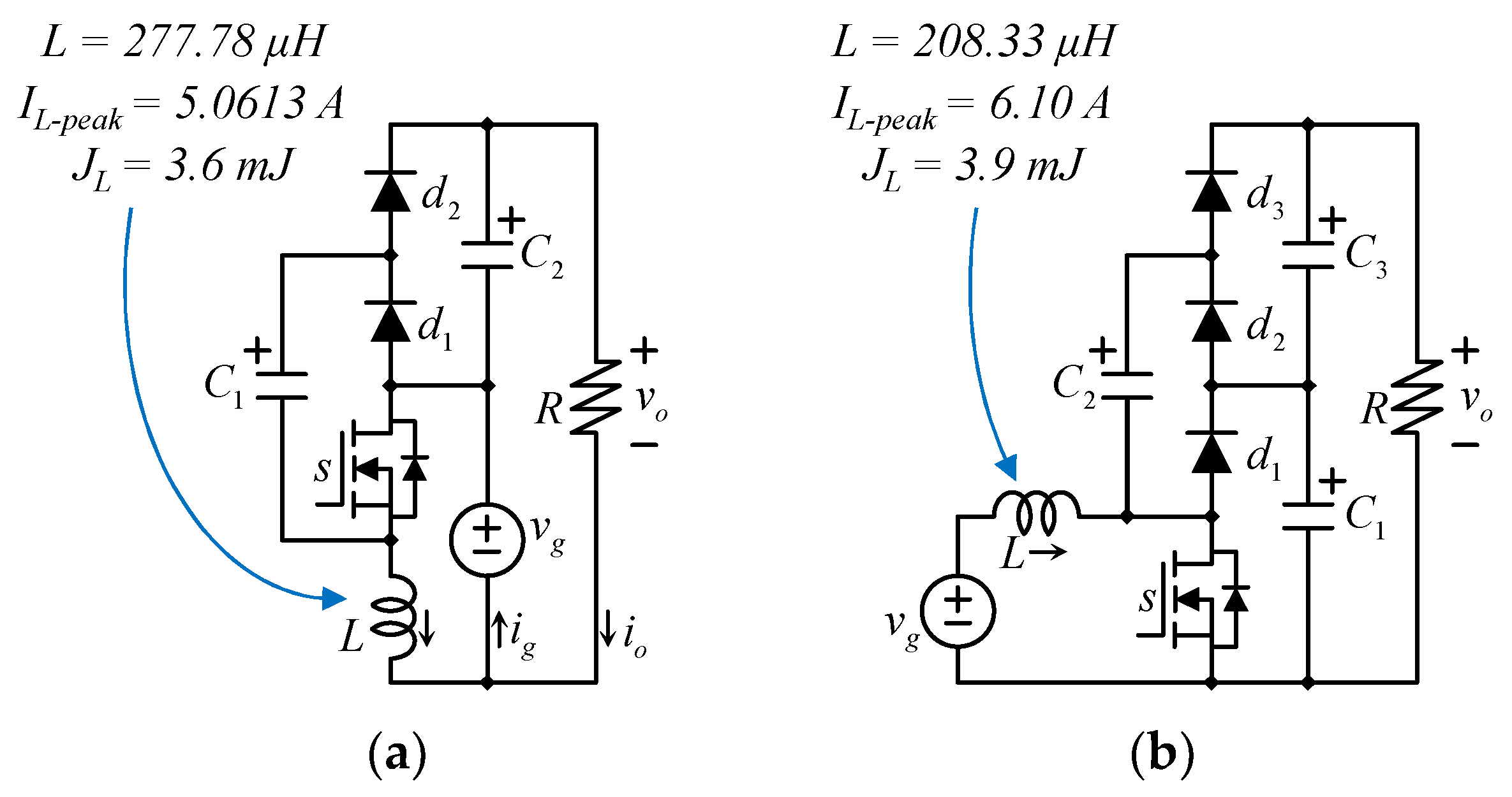
Next, the proposed RIC-MBC converter is compared with the state-of-the-art MBC converter. The MBC shown in
Figure 6b has been considered for the comparison as it is a very competitive topology and has become very popular among practitioners recently [
12,
13,
14,
15,
16,
17,
18,
19,
20,
21,
22,
23]. In particular, the single-inductor single-transistor topology with a continuous input current is considered, where the converter must be able to get in an interleaved connection (if required). The same conditions as before are considered, i.e., the converters must boost an input voltage fluctuating between 36 V and 50 V to an output regulated to 200 V. In this case, the 3-level MBC requires an inductor of 208 μH and drains a peak current of 6.10 A. The input voltage source is series connected with the inductor, and therefore, the peak current is identical to that of the classical boost, but its inductance is smaller (considering identical input current ripple and operating conditions). In fact, the inductance is lower than both the traditional boost and the proposed RIC-MBC converter (but the proposed one still drains a lower current, resulting in a lower stored energy). Additionally, the semiconductors and capacitors of the 3-level MBC are rated to 100 V, which is smaller than in the proposed RIC-MBC converter (164 V).
In retribution, the proposed RIC-MBC has fewer components. Notice that the MBC requires one additional diode and one additional capacitor. Certainly, the inductor of the 3-level MBC has less inductance; however, it drains a larger current. Out of this, the inductor in the 3-level MBC stores 3.9 mJ, while that of the proposed RIC-MBC converter yields 3.6 mJ, and thus a core with a larger volume is required in the 3-level MBC.
In the case of capacitors, the proposed RIC-MBC has an additional advantage. It requires only 50% of the stored energy to achieve the 0.2 V of the peak-to-peak output voltage ripple. The MBC requires 1.64 J, for having the same voltage ripple at the output port. In consequence, the proposed RIC-MBC requires two capacitors of 30 μF each, while the MBC requires all three capacitors of 106 μF. This can be easily verified with a computer simulation of the converters with the described operating conditions.
5. Extending the Topology to a Family
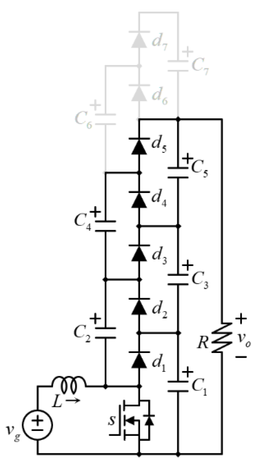
The traditional Multilevel Boost Converter (MBC) seems like an expanded traditional boost converter. The expansion looks like a voltage multiplier based on a diode–capacitor array. The diode–capacitor array can be extended to obtain more levels and, thus, a larger voltage.
Figure 7 shows an MBC with four levels, sometimes referred to as a 3×. It can be seen in gray how it can be extended to generate additional levels.
Following a similar approach, the proposed RIC-MBC can also be extended to generate more levels, leading to a full family of multilevel DC–DC converters.
Figure 7 shows the extended RIC-MBC.
In fact, as shown in
Figure 8, the proposed RIC-MBC could be considered as a new MBC family member since its characteristics and similarities with advantages can be summarized as follows: the inductor drains a smaller amount of current (still has a non-pulsating input current); an inductor with a lower current has a smaller size because the size is directly related to the capacity to store energy [
5,
24]; and its stored energy is proportional to the square of its current. Furthermore, the transistor drains the inductor current when it is closed. The reduction in the inductor current also reduces the transistor current stress. The RIC-MBC also requires less component count than the MBC for the same number of levels, and the comparative evaluation showed that the 3-level RIC-MBC requires capacitors with a smaller stored energy as compared to the 3-level MBC.
These similarities inspired the name of Reduced Inductor Current (RIC) Multilevel Boost Converter (MBC).
Comparison for a Particular Design
Table 1 shows the gains, duty cycles, and rated voltages required in all semiconductors and capacitors of the converters under consideration, namely the traditional (two levels) boost ones and the topologies of three and four levels for the MBC and RIC-MBC above discussed. All these converters must boost the voltage from 50 V to 200 V.
Evidently, the traditional boost requires a high-duty cycle at the rated power, which would be a design reason to discard it. The other converters require a smaller duty cycle.
Since all duty cycles at a rated power are different, the inductors of each converter would be different as well.
Table 2 shows each case’s inductance
L, peak current
iLmax, and stored energy
EL in the inductor.
All converters are designed to have the same current ripple at the input port. This can be simulated with any power electronics software for verification purposes; the inductance is the minimum to comply with the design specification, and the operating condition gives the peak current.
In summary, it can be seen from
Table 1 that the proposed converter has a larger voltage gain compared to the traditional boost converter. Furthermore, from
Table 2, it can be observed that the proposed converter has a smaller inductor current compared to the traditional boost and also compared to the multilevel boost converter. Those advantages are key contributions to the RIC-MBC.
The MBC and the boost converter have their inductors in series with the input supply. This explains why the maximum current at a rated power is the rated current (8.5 A) plus the current ripple (0.85 A or 10%). However, the proposed RIC-MBC requires a smaller current through the inductors. Recall that the stored energy is proportional to the square of the current; hence, a small reduction in the current results in a considerable reduction in the stored energy.
Figure 9 shows a comparison of the voltage gain of the traditional boost, the proposed RIC-MBC, and the MBC topology for the different levels considered. Notice that the proposed 3-level RIC-MBC (
Figure 6a) requires a reduced number of components compared to the 3-level MBC (
Figure 6b). The 3-level RIC-MBC requires a capacitor and two diodes less for the same number of levels at the output voltage compared with the 3-level MBC. The voltage gains (see
Figure 9) seem to have consistency with the number of devices on each topology, which explains why they are all considered members of the same family.
In all cases, the current ripple at the input port has the same mathematical expression (22):
By clearing the value of the inductor, it yields to:
Hence, topologies that require a smaller duty cycle for the same voltage gain require a smaller inductance in the input inductor. In all cases, the current ripple at the input port is equal to the one in the inductor (23).
Figure 10 shows the normalized input current ripple of the converters with the inductors shown in
Table 2 and an output power of 200 W. In all cases, the maximum normalized input current ripple is 15%, which is the design specification.
Notice that converters do not require an inductor with the same inductance for the same voltage gain since a topology with a larger gain requires a smaller duty cycle for the same voltage gain. In this sense, a larger voltage gain converter will always require a lower inductance, but this does not mean that the inductor would be smaller. In what follows, the stored energy is analyzed in more detail for a better understanding.
Another advantage of the proposed converter can be observed in
Figure 6,
Figure 7 and
Figure 8. Due to that, the inductor in the MBC is connected in series with the input voltage, the inductor current is the same as the input current, and the input current is the largest current in a step-up converter. On the other hand, the RIC-MBC has the inductor ground connected, and its current is equal to the current at the input minus the current at the output. This can be observed from the reference node in
Figure 6a or
Figure 8 and by invoking KCL. This results in a smaller current through the inductor, compared to the one at the input port and then also compared to the MBC and the classical boost (for equal operating conditions). A reduction in the current in an inductor leads to a reduction in the required core size (lower inductance and lower current). See
Table 2.
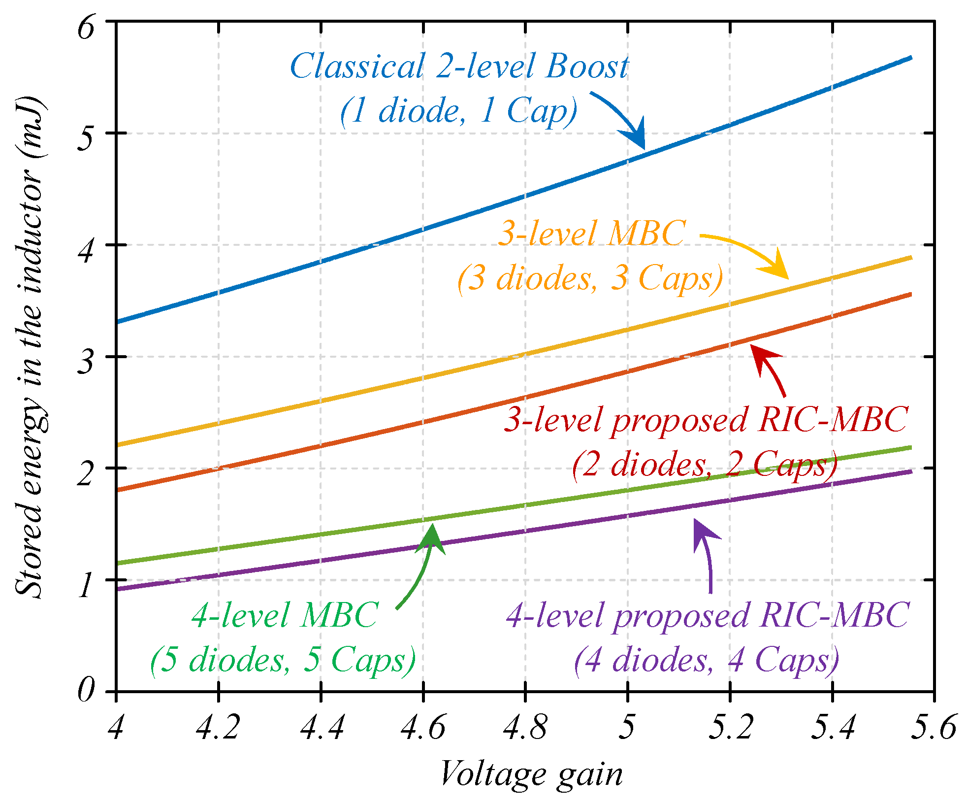
Figure 11 shows a graph of stored energy in the inductor vs. the voltage gain for the full range of operation, not only on the 36 V to 200 V operating point.
The conditions in this study considered a range of the input voltage to be between 36 V and 50 V and an output of 200 V, which represents a voltage gain in the range of 4 to 5.6.
Table 2 reveals that the proposed RIC-MBC requires an inductor that stores less energy. Additionally, as discussed above, it requires fewer components (a diode and a capacitor). The input voltage is given in a range, as a normal design criterion, since the converter must be prepared to work under conditions that can be caused by external conditions, such as changes in sun radiation due to climate conditions. This kind of change is handled with the converter controller, which adjusts the duty cycle to maintain a constant output voltage.
We have mentioned that if the current drain in an inductor is reduced, we can reduce the core size. Another option is to keep the core size but increase the number of turns (for example, in a toroidal core), which would increase the inductance and a further reduction in the current ripple.
6. Experimental Results
An experimental test bench was built to test the 3-level RIC-MBC (see
Figure 3) and to corroborate its operations and advantages.
Table 3 shows the devices and parameters used in the experiment; the test bench was built based on the TDHB-65H070L-DC Gallium Nitride transistors evaluation board by Transphorm.
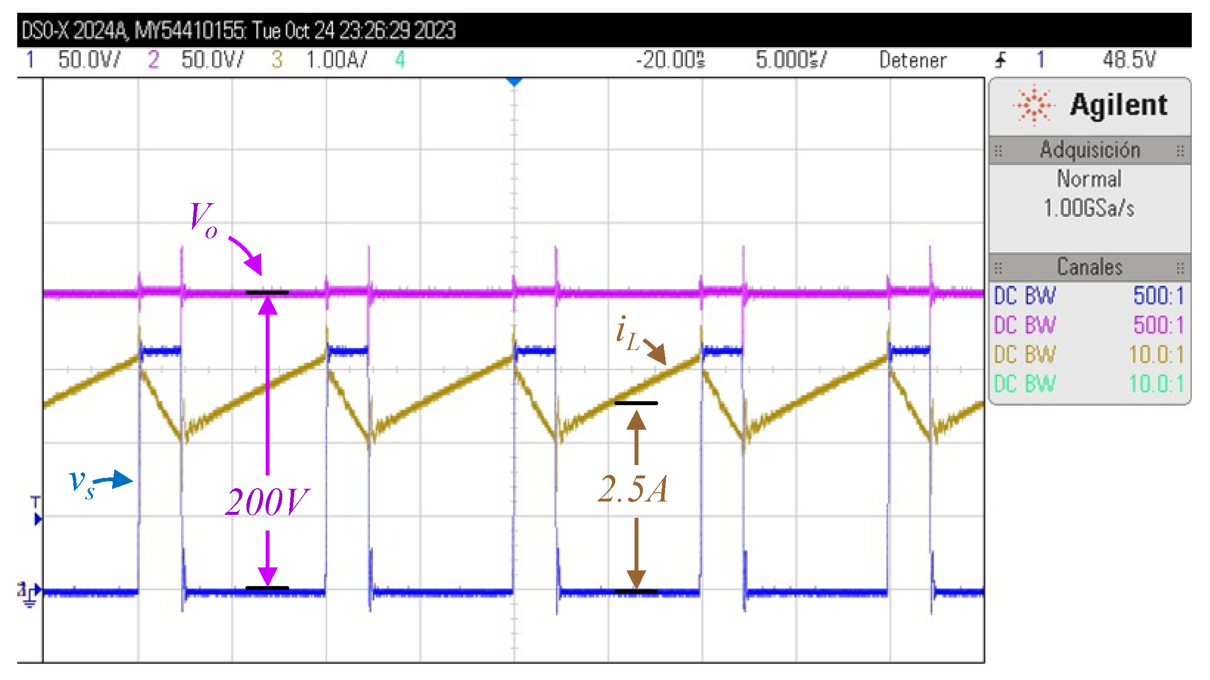
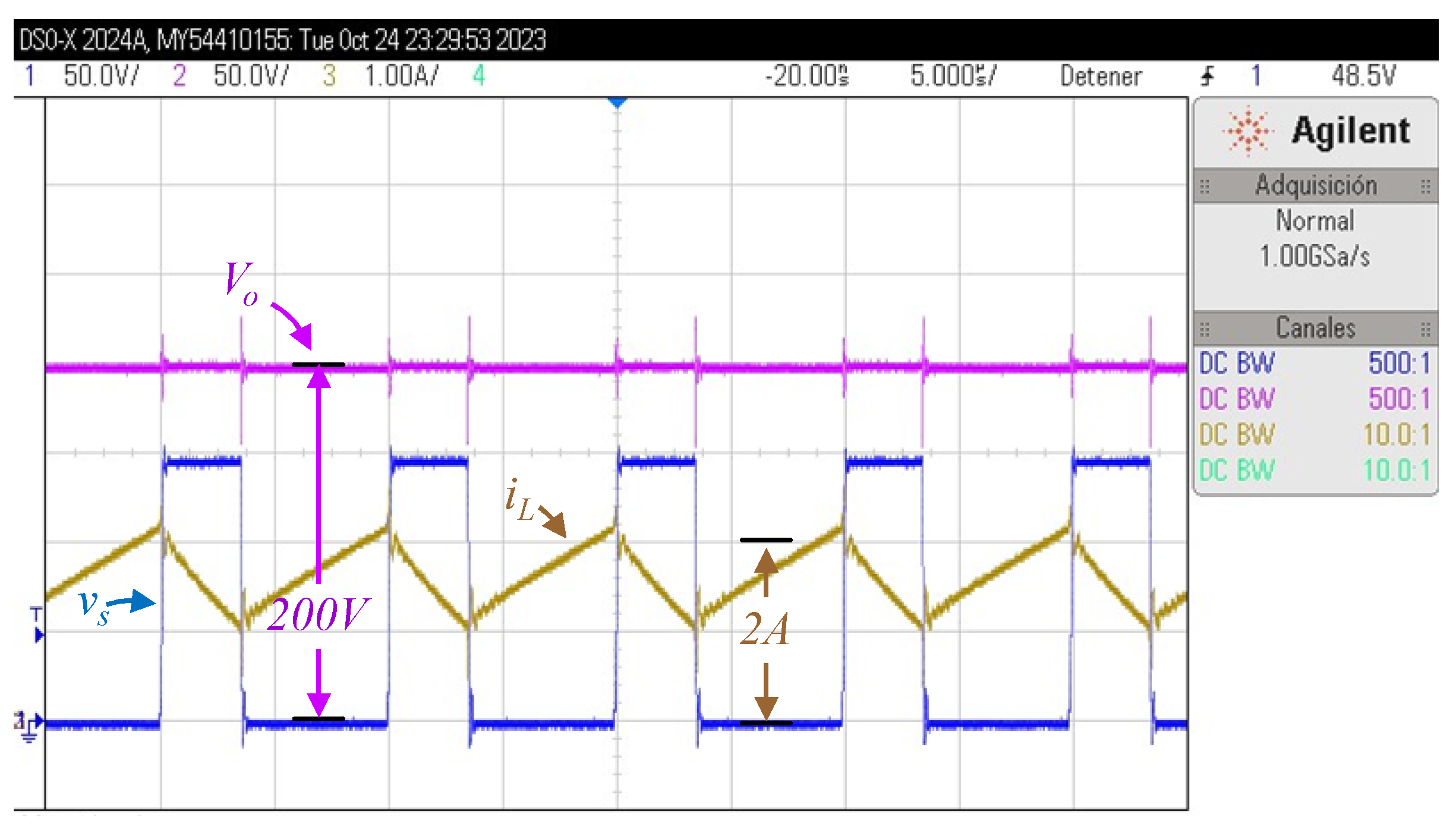
Figure 12,
Figure 13 and
Figure 14 show in dark yellow the current through the inductor (
iL) at 1A per division, the voltage at the output port (
vo) in a purple color at 50 V per division, and the switch voltage (
vs) in a blue color also at 50 V per division. The prototype has both equal capacitors of 10 µF and a 250 µH inductor.
The switching frequency was chosen at 100 kHz. The experiments consider 200 V as the output voltage with different input voltages (
Vg values), particularly 35 V (
Figure 12), 45 V (
Figure 13), and 50 V (
Figure 14). The obtained results are as expected and coincide with the theory and equations. In these figures, the time axis has 5 µS per division.
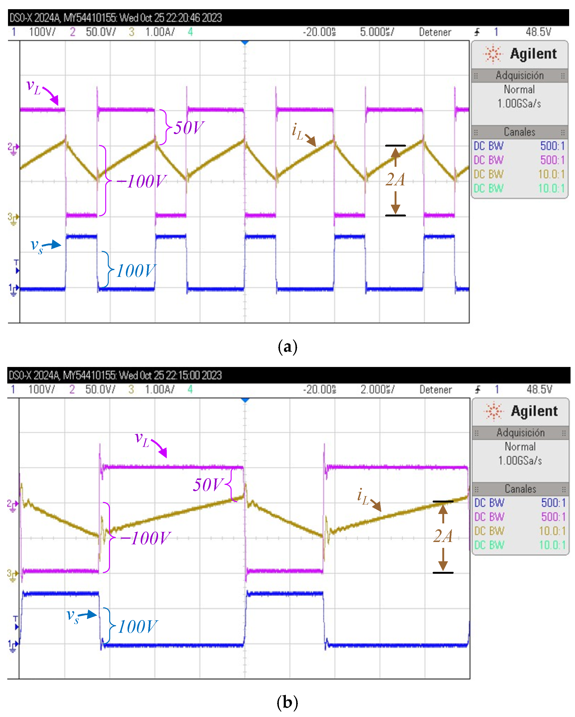
Figure 15a shows in dark yellow the current through the inductor (
iL) at 1 A per division, the voltage at the inductor (
vL) in a purple color at 50 V per division, and the switch voltage (
vs) in a blue color also at 100 V per division.
In
Figure 15, the switch signal was used to provide the trigger for the oscilloscope. The inductor voltage seems to be 50 V when the switch is on, and its current is rising. On the other side, when the switch is off, the inductor voltage seems to be −100 V, which is according to the equivalent circuits in
Figure 4.
The output voltage is 200 V as expected, while the input current seems to have a triangular waveform in which the ripple depends mainly on the inductance. The switch voltage seems like a pulse train that is opposite to the switching signal, since the transistor has nearly zero voltage when the switching signal is high, and the transistor is closed. The duty cycle can be estimated from this signal, and it was estimated around 0.78 for
Figure 12, 0.70 for
Figure 13, and 0.66 for
Figure 14, which is expected from the converters’ voltage gain.
Losses and Efficiency Computation
The power losses in each element and the total efficiency were calculated, considering the input as
Vg =
50 V, the output as
Vo =
200 V, and the output power varied from 20 to 200 W. The switching frequency considered was 100 kHz. The resulting efficiency is shown in
Figure 16.
Figure 17 shows a power loss breakdown for
Vg = 50 V,
Vo = 200 V, a switching frequency of 100 kHz, and
Po = 200 W. The capacitors used were film capacitors with an ESR = 5 mΩ. The losses in the capacitors were very small and appear as a negligibly small portion between the power losses at the inductor
L and the power losses of the switch
s.
The prototype used film capacitors with a very small ESR (5 mΩ). It is recommended not to use electrolytic capacitors since the RMS current in capacitors was calculated as 1.63 A, which may cause a large amount of power loss in electrolytic capacitors.
7. Conclusions and Future Work
This article introduced a DC–DC converter, which is called a Reduced Inductor Current Multilevel Boost Converter (RIC-MBC). It can be considered a new multilevel boost converter (MBC) family member, as it shares several properties with other ones. However, the proposed RIC-MBC exhibits the following advantages as compared to the MBC topology: it requires fewer components for the same voltage levels, the inductor drains less current, and thus it stores less energy. The size of the inductor is related to its stored energy, which is proportional to its peak current. A description of the converter was provided along with a comparative evaluation; the comparison includes the classical boost topology and the multilevel boost converter. A comparative evaluation with a converter design was performed to demonstrate the advantages of the proposed converter. For a particular design, the proposed converter required an inductor of 277.78 μH for a peak current of 5 A. The traditional boost converter required an inductor of 312.50 μH for a peak current of 6 A. The proposed converter required 63% of the stored energy in the inductor. An experimental test bench was built, and experimental results are presented in this article to prove the proposition’s concept.
In future work, several aspects of the converter will be investigated, such as the controller design, the operation with different capacitances in the capacitors, their design from the optimization point of view, and the discontinuous conduction mode.


 ,
, 


