1. Introduction
Wide-bandgap semiconductors, notably Gallium Nitride (GaN), have revolutionized the field of power electronics. GaN power devices represent a transformative leap from traditional silicon-based counterparts due to their exceptional electrical properties, making them a promising solution for the ever-growing demand for more efficient, compact, and high-performance electronic systems [
1]. The primary advantage of GaN lies in its exceptional material properties, which encompass a wide bandgap (3.4 eV), high electron mobility, and a substantial breakdown field. These attributes lead to reduced conduction losses and enhanced switching capabilities, enabling GaN devices to function efficiently at elevated frequencies and temperatures and rendering them well-suited for a wide range of power applications.
AlGaN/GaN heterojunctions exhibit two-dimensional electron gas (2DEG) channels at the interface between AlGaN and GaN, featuring high electron densities typically in the range of 10
13 cm
−2, a result of spontaneous and piezoelectric polarization effects [
2]. Nevertheless, it is imperative to acknowledge that these pronounced polarization effects present a challenge for enhancement-mode (E-mode) operation. E-mode operation in GaN power devices is of paramount importance in power electronics applications. It allows for easy control of the device. In E-mode, the transistor is normally off at zero gate voltage, which simplifies the device’s behavior and ensures a default state of non-conduction. This is particularly advantageous in power management applications where precise control of power flow and on/off switching is crucial. E-mode operation also minimizes power consumption when the device is in standby or off states, reducing wasted energy and increasing overall efficiency. This is especially critical in modern power electronics, where energy efficiency is a primary concern. In the pursuit of E-mode operation in GaN power devices, various techniques have been developed with the common objective of depleting the 2DEG channel beneath the gate region at zero gate voltage [
3,
4,
5,
6,
7,
8]. An example of this progress is the availability of commercially accessible p-GaN gated AlGaN/GaN heterojunction field-effect transistors (HFETs). In this structure, the p-GaN layer, denoting p-type GaN, serves as the gate region that can be turned on or off by applying a voltage to control the flow of electrons in the channel. Positioned beneath the p-GaN layer is an AlGaN barrier layer, which is engineered to have a wide bandgap and acts as a barrier between the p-GaN and the 2DEG channel. Subsequently, located beneath the AlGaN layer, there exists a GaN channel layer, forming the 2DEG channel between the AlGaN and GaN layers.
The fabrication of a p-GaN gated AlGaN/GaN HFET can be accomplished typically through either a p-GaN etching process or a p-GaN epitaxial regrowth process [
9,
10,
11,
12]. The p-GaN etching process is more commonly employed, as the regrowth process entails a more intricate procedure. The regrowth process involves etching the AlGaN layer under the gate region, followed by the regrowth of the p-GaN or p-GaN/AlGaN layer. Therefore, the interface quality between the upper regrown layer and the etched surface is critical. After regrowth, the region outside the gate area must undergo etching to remove the p-GaN layer, as the p-GaN layer is necessary only for the gate area. This etching process is less sensitive than in cases that do not employ the regrowth process, because the AlGaN layer thickness can be independently designed, unlike in conventional E-mode p-GaN/AlGaN/GaN epitaxial structures. Thus, slight over-etching does not significantly affect the device characteristics. Therefore, the advantage of the regrowth process is the high 2DEG channel density in the etched AlGaN/GaN region, which can reduce the on-resistance. However, the disadvantage is the complex wafer process and higher cost; the wafer must undergo the epitaxial growth process again during fabrication. From a fabrication standpoint, the etching process is simpler than the regrowth process if the etch depth is precisely controlled. The typical epitaxial structure utilized for the p-GaN gated E-mode HFET comprises p-GaN/AlGaN/GaN where the thickness of the p-GaN layer is at least several tens of nm and the AlGaN barrier beneath the p-GaN layer ranges between 10 nm and 15 nm. When subjecting the p-GaN layer to a plasma-based etching process, it is crucial to precisely control the depth of p-GaN etching while minimizing plasma-induced damage. Given the thinness of the AlGaN barrier layer, even slight over-etching of the AlGaN layer or plasma-induced damage at the etched surface can substantially reduce the 2DEG channel density, increasing the on-resistance. Thus, research efforts have been dedicated to selectively etching the p-GaN layer, utilizing either oxygen-based processes [
13,
14,
15,
16,
17] or fluorine-based plasma etching [
18,
19,
20,
21,
22]. In the context of the selective etching process, the inclusion of an over-etching step is essential to guarantee the complete removal of the p-GaN layer. This over-etching step exposes the AlGaN surface to plasma bombardment. Consequently, the optimization of the selective etching process necessitates a meticulous examination of both selectivity and plasma-induced damage.
In this study, we have developed a low-damage, fluorine-based selective etching process for the fabrication of E-mode p-GaN gated AlGaN/GaN HFETs. We conducted a comprehensive investigation into the effects of various etching process parameters, including SF6 gas concentration, chamber pressure, bias power, and ICP power. The optimized process recipe was effectively utilized to demonstrate an E-mode device with promising characteristics.
2. Selective Etching Process Optimization
We designed a fluorine-based selective etching process using a gas mixture comprising BCl3 and SF6. Our optimization efforts focused on investigating several process parameters, including gas concentration, chamber pressure, bias power, and ICP power. The process optimization sequence unfolded as follows: The most pivotal parameter in selective etching is the fluorine concentration, which plays a crucial role in halting the etching process at the AlGaN surface. Our initial step involved determining the highest selectivity condition for the fluorine concentration within a total gas flow rate of 40 sccm. The initial conditions for the other process parameters were a chamber pressure of 20 mTorr, a bias power of 20 W, and an ICP power of 600 W, all conducted at a fixed chamber temperature of 60 °C. After identifying the optimal fluorine concentration, we then varied the chamber pressure to enhance selectivity. Our target selectivity was set at a minimum of 10:1 (p-GaN:AlGaN) and ideally exceeding 20:1. During the etching phase, we monitored the DC-bias voltage as an indicator of plasma-induced damage. The DC-bias voltage reflects the acceleration of positive ions towards the surface, a major contributor to surface damage. Consequently, the DC-bias voltage measured during the etching process plays an important role in determining the process conditions. Both the etch rate and the DC-bias voltage exhibit strong dependencies on chamber pressure and bias power. To maintain high selectivity while reducing the DC-bias voltage, we systematically varied chamber pressure, bias power, and ICP power within wide ranges. The experiments are elaborated upon in detail in the following sections.
2.1. Effects of SF6 Gas Concentration
During the etching process, when the AlGaN surface is exposed to a fluorine-based plasma environment, the interaction between aluminum (Al) and fluorine (F) leads to the formation of an etch-resistant aluminum fluoride (AlF
x) layer, acting as an etching barrier [
21]. However, fluorine can also react with gallium (Ga) in the p-GaN, resulting in the formation of involatile gallium fluoride (GaF
x) [
22]. An excess of fluorine, leading to the dominance of GaF
x, can reduce the etch rate for the p-GaN layer and compromise selectivity. Therefore, the fluorine concentration in the gas mixture is a critical parameter in the selective etching process.
Selective etching experiments were conducted using p-GaN and Al
0.2G
0.8N layers under the following conditions: chamber pressure of 20 mTorr, bias power of 20 W, ICP power of 600 W, chamber temperature of 60 °C, and a total gas flow of 40 sccm. The gas mixture comprised BCl
3 and SF
6, with varying gas ratios.
Figure 1a shows the etch rates for GaN and AlGaN as a function of the SF
6 ratio, while
Figure 1b presents the DC-bias voltage measured during the etching process and the selectivity between p-GaN and AlGaN. In
Figure 1a, the etch rate for p-GaN increases as the SF
6 ratio rises, while the etch rate for AlGaN remains relatively constant with changes in the gas ratio. The peak etch rate for GaN was achieved with a gas ratio of BCl
3:SF
6 = 65:35, resulting in a selectivity of p-GaN:AlGaN = 4.5:1. The DC-bias voltage measured during the etching process decreased with an increasing SF
6 ratio.
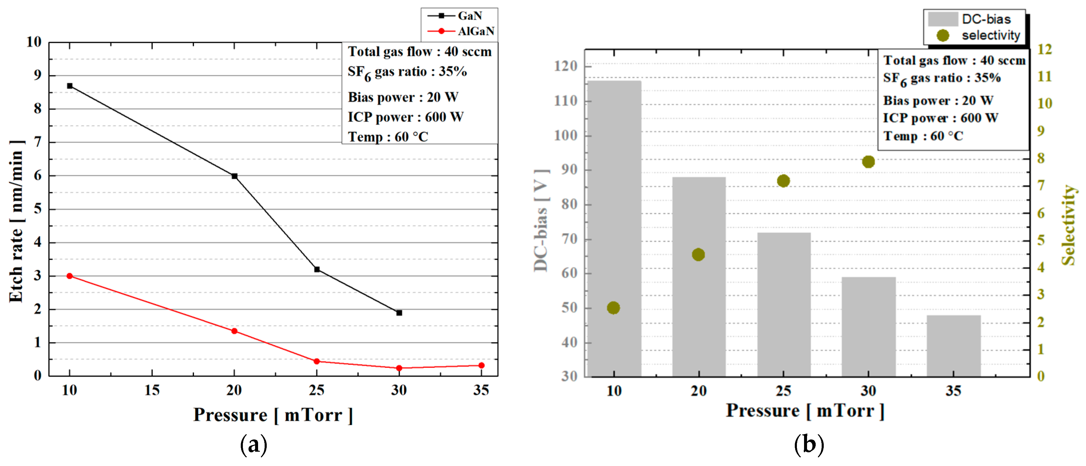
2.2. Effects of Chamber Pressure
The impact of chamber pressure was investigated using an SF
6 gas ratio of 35%, which provided the highest selectivity. Chamber pressure was varied from 10 mTorr to 35 mTorr, while other conditions remained consistent with the previous experiments. As shown in
Figure 2, both p-GaN and AlGaN etch rates decreased as chamber pressure increased.
Figure 2b demonstrates that the DC-bias voltage exhibited a similar trend. Higher chamber pressure enhances reactivity with fluorine, generating more AlF
x and GaF
x compounds, which in turn reduces the etch rate. It is noteworthy that no further reduction in the etch rate for AlGaN was observed beyond a chamber pressure of approximately 30 mTorr. The highest selectivity of p-GaN:AlGaN = 8:1 was achieved at a chamber pressure of 30 mTorr, with etch rates for p-GaN and Al
0.2Ga
0.8N of 1.9 nm/min and 0.24 nm/min, respectively.
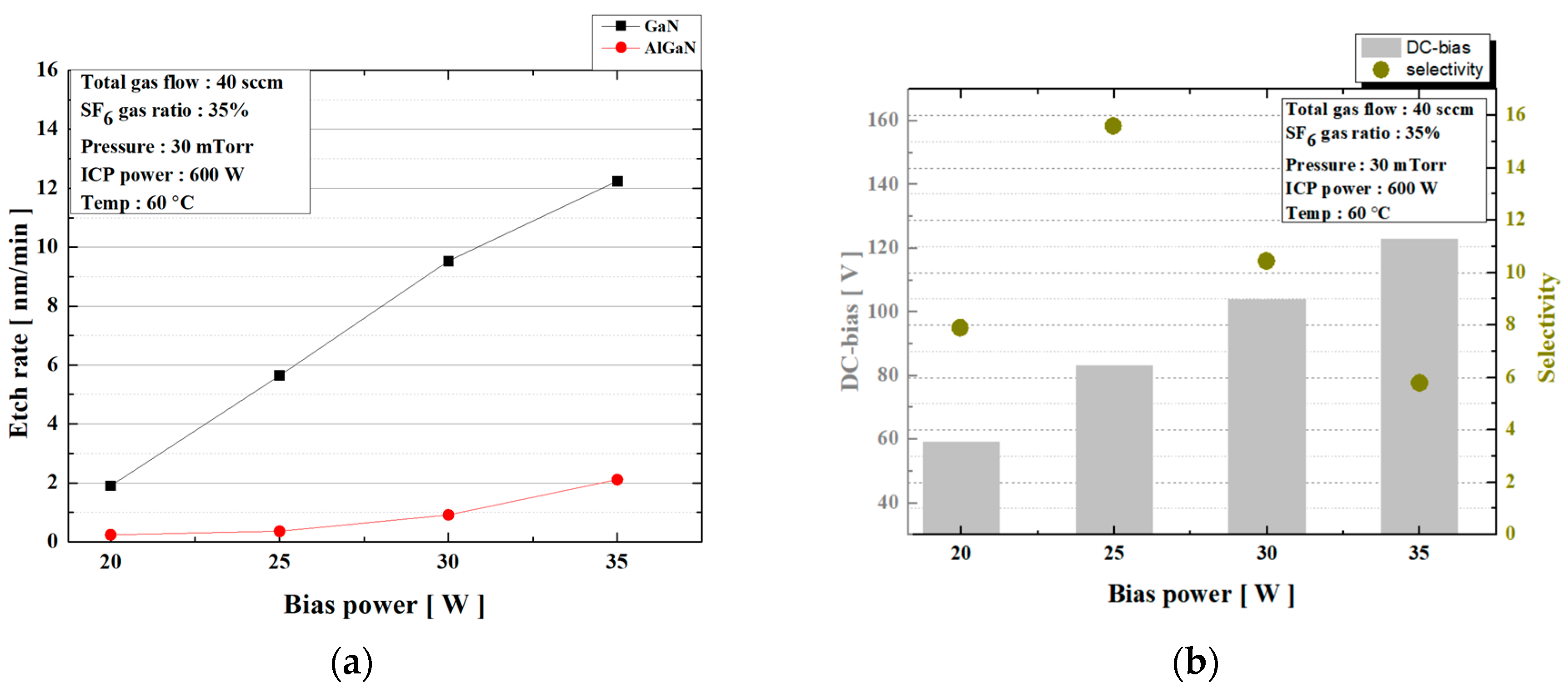
2.3. Effects of Bias Power
The effects of bias power were investigated under the following etching conditions: SF
6 ratio of 35%, chamber pressure of 30 mTorr, ICP power of 600 W, and chamber temperature of 60 °C. Bias power was varied from 20 W to 35 W.
Figure 3 illustrates that the etch rates and the DC-bias increased with increasing bias power. The highest selectivity was achieved at a bias power of 25 W, resulting in etch rates for p-GaN and Al
0.2Ga
0.8N of 5.46 nm/min and 0.36 nm/min, respectively. The DC-bias voltage measured during the etching process was 80 V.
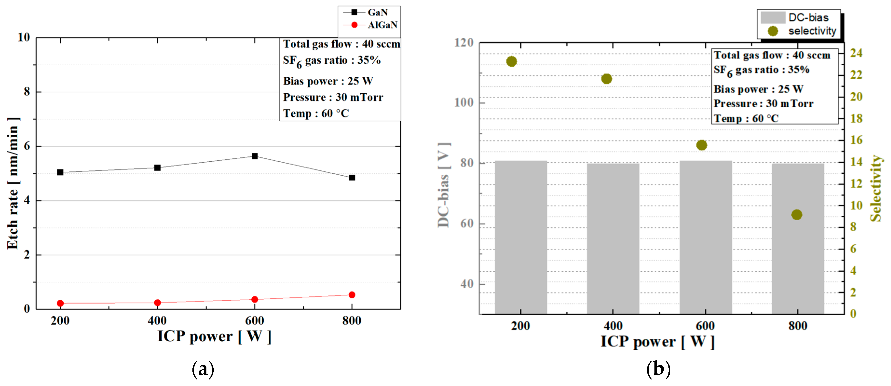
2.4. Effects of ICP Power
Finally, the impact of ICP power was investigated by varying it from 200 W to 800 W under the etching conditions of an SF
6 ratio of 35%, chamber pressure of 30 mTorr, bias power of 25 W, and chamber temperature of 60 °C. The resulting etch rates and measured DC-bias voltage are plotted in
Figure 4a,b. While no significant change was observed in the DC-bias voltage, the etch rate for AlGaN slightly increased with higher ICP power, leading to a reduction in selectivity. The highest selectivity of p-GaN:AlGaN = 23:1 was achieved with an ICP power of 200 W. Although there was a small difference in selectivity between 200 W and 400 W, the surface roughness after etching with an ICP power of 400 W was better than at 200 W, with surface roughness values of 0.806 nm and 1.148 nm, respectively. Therefore, an ICP power of 400 W is recommended.
Based on these experiments, the optimal etching process conditions were determined as follows: SF6 gas ratio of 35% (i.e., BCl3:SF6 = 26:14 sccm), chamber pressure of 30 mTorr, bias power of 25 W, ICP power of 400 W, and chamber temperature of 60 °C. These conditions resulted in an etch selectivity of p-GaN:AlGaN = 21:1 (i.e., p-GaN:Al0.2Ga0.8N = 5.2:0.25 nm/min).
3. Comparison of Selective Etching Processes
Earlier, we reported on an oxygen-based selective etching process with optimal conditions, including a gas flow rate of Cl
2/N
2/O
2 = 40/10/2 sccm, a chamber pressure of 20 mTorr, an ICP power of 2000 W, a bias power of 25 W, and a chuck temperature of 60 °C [
17]. This process resulted in significantly higher selectivity of p-GaN:AlGaN = 53:1 compared to the fluorine-based etching process developed in this study, which was p-GaN:AlGaN = 21:1. However, the oxygen-based etching process required very high ICP power, which could potentially cause more damage to the etched surface. The ICP power for the oxygen-based process was five times higher than that for the fluorine-based process. As a result, the DC-bias voltage measured during the etching process was 198 V for the oxygen-based selective etching process, which was more than two times higher than that for the optimum fluorine-based selective etching process (i.e., 80 V).
We investigated the effects of each etching process on the electrical characteristics of etched AlGaN/GaN heterostructures prepared by two different selective etching processes. The initial epitaxial structure consisted of p-GaN/Al0.2Ga0.8N/GaN, with a p-GaN thickness of 70 nm and an AlGaN thickness of 15 nm. The p-GaN layer was selectively etched by either an oxygen- or a fluorine-based selective etching process, followed by the formation of ohmic contacts and mesa isolation.
Firstly, Hall measurements were conducted to determine the sheet resistance and 2DEG concentration for both samples. The Hall measurement pattern was fabricated on the selectively etched AlGaN surface, which featured four ohmic electrodes at the corners of a square-shaped channel area of 450 × 450 μm
2. The measurement results are summarized in
Table 1. The oxygen-based selective etching process resulted in a sheet resistance of 2147 Ω/□ and a 2DEG concentration of 4.4 × 10
12/cm
2, while the fluorine-based process resulted in a sheet resistance of 978 Ω/□ and a 2DEG concentration of 5.9 × 10
12/cm
2. Due to the selective etching process, the thickness of the remaining AlGaN barrier layer was consistent in both samples. Consequently, the difference resulted from plasma-induced damage at the surface, where damage-induced trap states play a significant role. Residual species, dangling bonds, and related surface-pinning effects can modify the 2DEG density and channel mobility. It is essential to note that the AlGaN layer is only 15 nm thick, making it highly sensitive to any alterations in surface conditions.
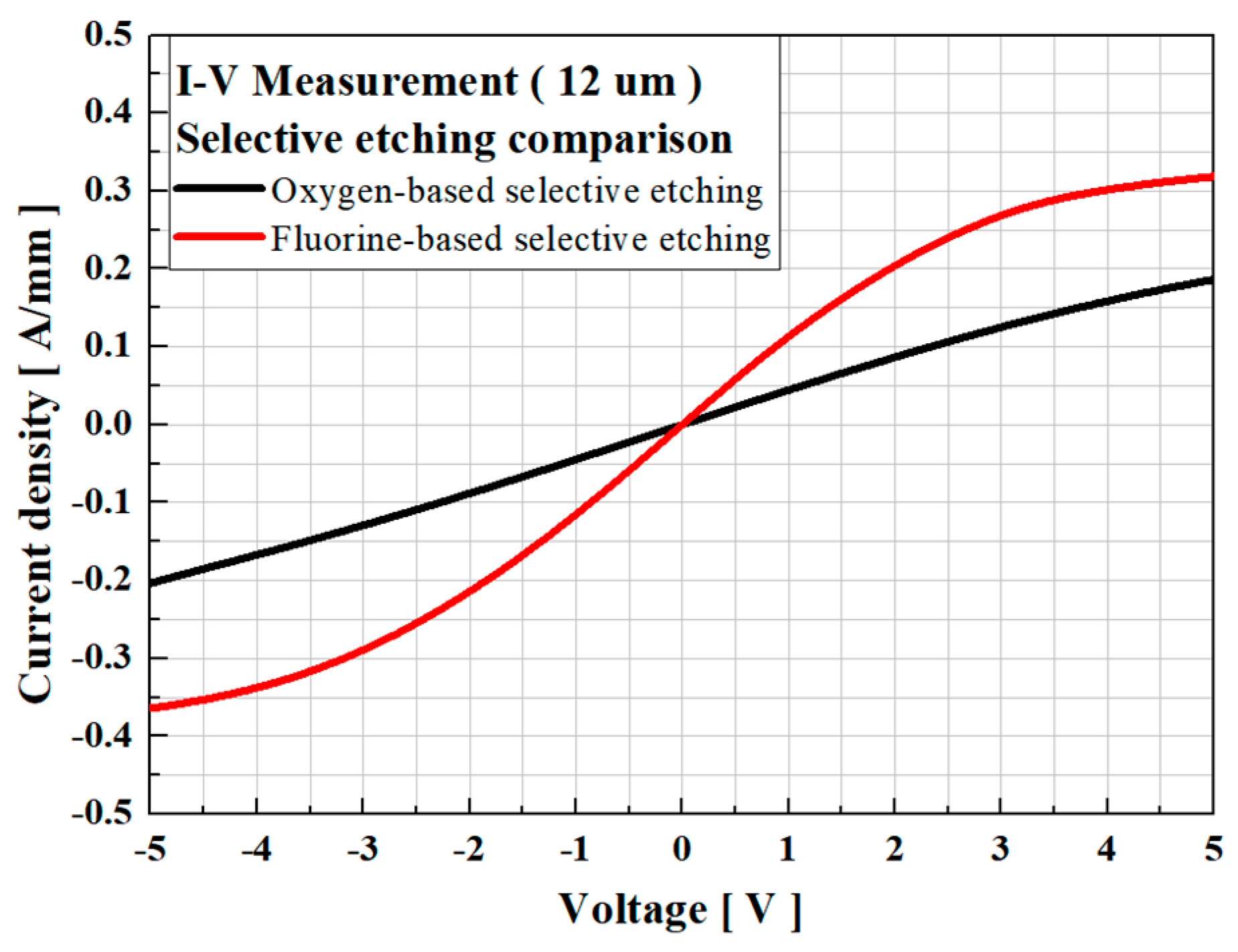
Secondly, the current–voltage (I–V) characteristics were also measured between two ohmic electrodes placed at a distance of 12 μm from each other. As illustrated in
Figure 5, the sample that was fabricated using the fluorine-based selective etching process exhibited a significantly higher current density when compared to the sample prepared using the oxygen-based process. Since the thickness of the AlGaN barrier layer remains consistent after the selective etching process in both samples, it is suggested that the superior I–V characteristics are associated with reduced surface damage.
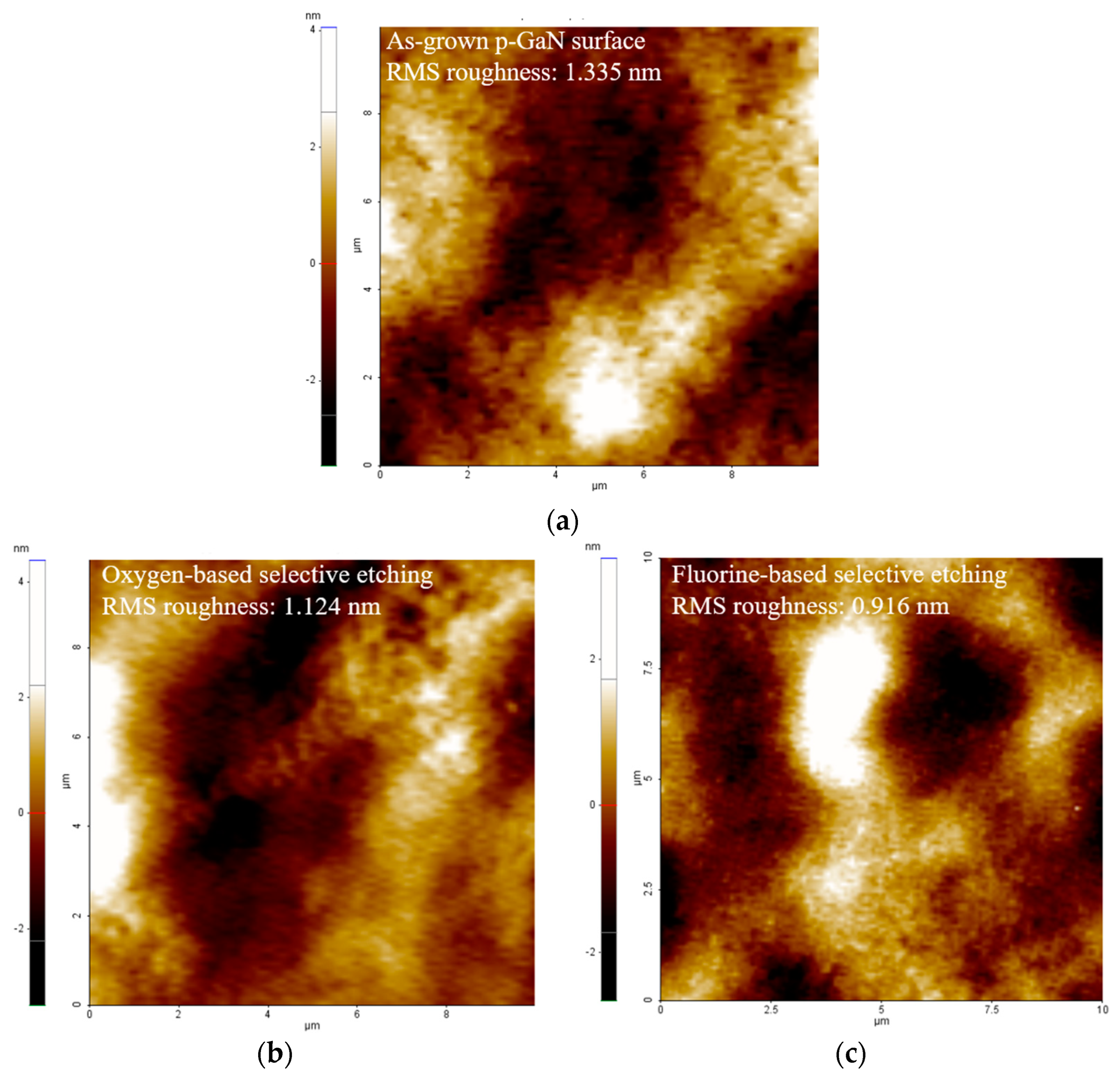
The etched surface of both samples was inspected using atomic force microscopy (AFM). The pristine surface before etching had an RMS roughness of 1.335 nm, shown in
Figure 6a. The etched surfaces of the samples fabricated using the oxygen-based and the fluorine-based selective etching processes exhibited roughness values of 1.124 nm and 0.916 nm, respectively, as shown in
Figure 6b,c. This noticeable improvement in surface roughness suggests a smoother etching process when using the fluorine-based etching process.
These findings indicate that while the oxygen-based selective etching process yields higher selectivity, it requires significantly higher ICP power, which causes significant damage to the etched surface and results in a higher sheet resistance. On the other hand, the fluorine-based selective etching process provides lower sheet resistance, higher 2DEG concentration, and improved surface morphology, making it a promising alternative with reduced plasma damage to the etched surface.
4. Device Fabrication Using Optimum Selective Etching Process
4.1. Device Fabrication
The optimized selective etching process was employed for the fabrication of E-mode p-GaN gated AlGaN/GaN HFETs. The epitaxial structure comprised a 70 nm p-GaN layer, a 15 nm Al
0.2Ga
0.8N barrier layer, a 200 nm GaN channel layer, and a 5.2 μm buffer layer grown on a 1 mm thick Si (111) substrate. The p-GaN layer was doped with Mg. After thorough solvent and acid cleaning, the p-GaN gate region was defined using photolithography, and the optimized fluorine-based selective etching process was applied to etch the p-GaN layer outside the gate area. After completing the selective etching process, the etch depth was verified using AFM. Then, the wafer was cleaned using sulfuric acid peroxide mixture (H
2SO
4/H
2O
2) followed by solvent cleaning. Buffered oxide etch (BOE) was used to remove native oxide from the surface prior to passivation. The surface was passivated using plasma-enhanced chemical vapor deposition (PECVD) to deposit a SiO
2 film at 350 °C [
23]. Au-free ohmic contacts were formed using a Ti/Al/TiN metal stack (=30/150/20 nm) followed by annealing at 550 °C in an N
2 ambient. The ohmic metal was in direct contact with the 2DEG channel, facilitated by the ohmic-recess etching process. MESA isolation was carried out using a BCl
3/Cl
2-based reactive-ion etching (RIE) process. From transmission line measurements, a transfer contact resistance of 0.94 Ω∙mm was obtained with a specific contact resistivity of 1.17 × 10
−5 Ω·cm
2. Next, the gate contact region on the p-GaN area was defined through an SF
6-based plasma etching process, and additional photolithography was employed to pattern the gate and pad electrodes. An Au-free TiN/Ti metal stack (=50/150 nm) was used for the Schottky gate and pad electrodes. The fabricated device had a source-to-p-GaN gate spacing of 3 μm, a p-GaN gate length of 4 μm, and a p-GaN gate-to-drain spacing of 12 μm, as illustrated in
Figure 7. The gate contact length on top of the p-GaN region was 2 μm. The reason for the relatively long gate length was due to limitations in the resolution and misalignment margin of the photolithography equipment used in this study.
4.2. Characterization of E-Mode p-GaN Gated AlGaN/GaN HFET
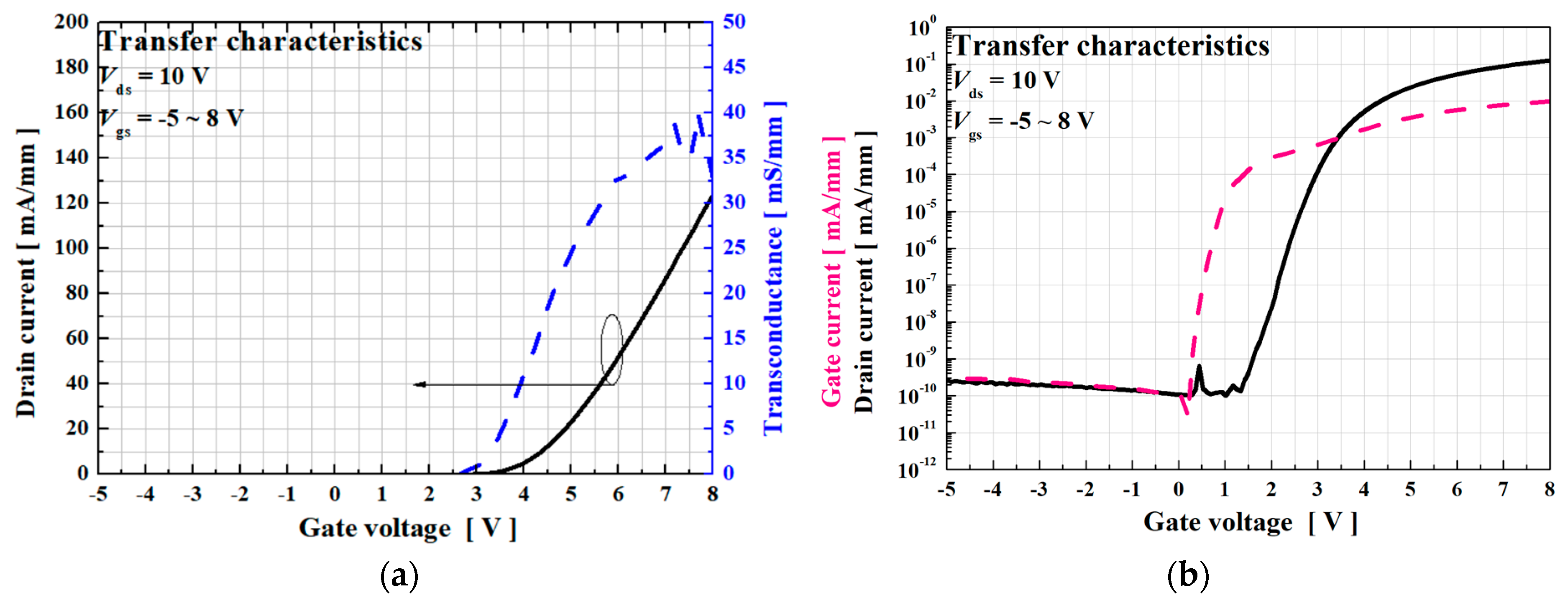
Figure 8 shows the measured transfer I–V characteristics of the E-mode p-GaN gated AlGaN/GaN HFET that was fabricated using the optimum fluorine-based selective etching process. These measurements were taken at a fixed drain voltage (V
ds) of 10 V. The device demonstrated notable performance metrics, including a threshold voltage of 3.5 V and an impressive on/off ratio of >10
9, achieved at a gate-source voltage (V
gs) of 8 V. Moreover, the off-state drain leakage current was remarkably low, measuring approximately 10
−10 A/mm.
Figure 9 shows a plot of the measured output I–V characteristics from which the specific on-resistance was extracted. The specific on-resistance extracted at V
ds = 2 V was 5.3 mΩ.cm
2. This extraction accounts for the intrinsic channel region between source and drain.
In order to investigate the trapping effects, a series of pulse measurements were carried out. These pulse measurements employed a precisely controlled pulse width of 1 μs and a repetition period of 1 ms.
Figure 10 shows the pulsed I–V characteristics measured at various quiescent drain bias voltages with a constant quiescent gate bias voltage of 0 V. It is noteworthy that, during these experiments, no significant current collapse was observed within the linear region of operation, indicating stable and reliable device performance under these conditions.
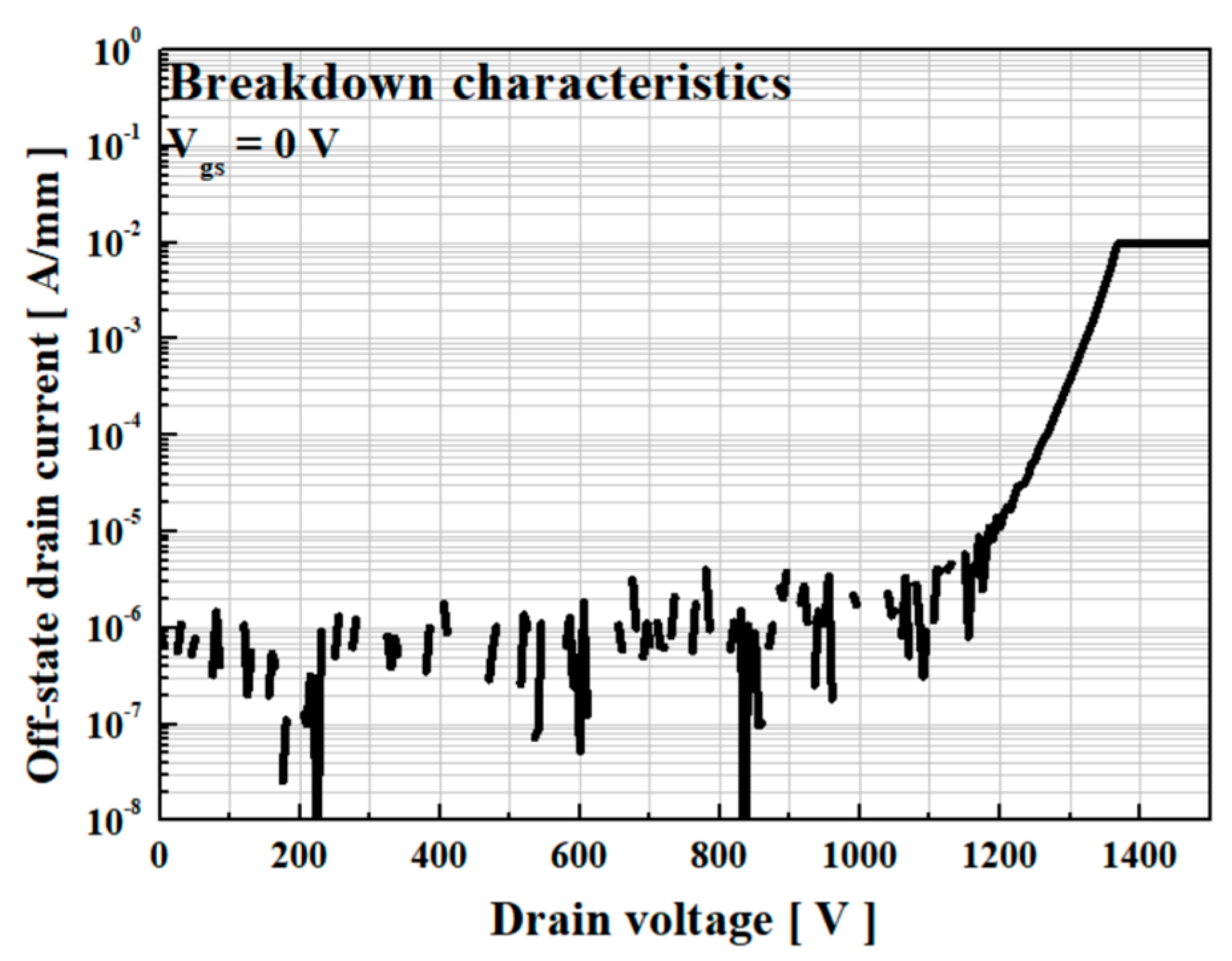
The off-state breakdown characteristics were measured at a gate voltage (V
gs) of 0 V using the Keysight B1505A system. As shown in
Figure 11, there was no breakdown phenomenon observed, even when subjecting the device to voltages as high as V
ds = 1000 V. Furthermore, the catastrophic breakdown voltage was found to exceed V
ds = 1350 V. The observed noisy leakage current level below V
ds = 1000 V is attributed to the resolution limitations of the equipment during high-voltage measurements. These extensive device characteristics underscore the promising performance exhibited by the fabricated E-mode p-GaN gated AlGaN/GaN HFET, encompassing attributes such as a high threshold voltage, exceptional on/off ratio, minimal leakage current, low on-resistance, and robust off-state breakdown characteristics. It is suggested that the fluorine-based etching process optimized in this study is a promising technique that can be utilized in the fabrication of E-mode p-GaN gated AlGaN/GaN HFETs.
5. Conclusions
This study has explored the optimization of a low-damage selective etching process for the fabrication of E-mode p-GaN gated AlGaN/GaN HFETs. A low-damage fluorine-based selective etching process was developed and optimized through a systematic investigation of various parameters. The critical parameters included SF6 gas concentration, chamber pressure, bias power, and ICP power. The optimized process conditions resulted in a remarkable etch selectivity of p-GaN:AlGaN = 21:1, with minimal damage to the etched surface. The optimal process conditions identified were as follows: an SF6 gas ratio of 35% (i.e., BCl3:SF6 = 26:14 sccm), a chamber pressure of 30 mTorr, a bias power of 25 W, an ICP power of 400 W, and a chamber temperature of 60 °C.
Comparisons were made with an oxygen-based selective etching process, which exhibited higher selectivity but required significantly higher ICP power and caused more damage to the etched surface. The fluorine-based process, on the other hand, yielded lower sheet resistance, higher 2DEG concentration, and improved surface morphology, offering promise as an alternative with reduced plasma damage.
The optimized selective etching process was applied to fabricate E-mode p-GaN gated AlGaN/GaN HFETs. These devices exhibited impressive characteristics, including a threshold voltage of 3.5 V, a specific on-resistance of 5.3 mΩ·cm2, an on/off ratio exceeding 109, and a low off-state drain leakage current of approximately 10−10 A/mm. Off-state breakdown tests demonstrated the robustness of the fabricated HFETs, with no breakdown observed up to 1000 V and a catastrophic breakdown voltage exceeding 1350 V.
In summary, this research has successfully optimized a low-damage fluorine-based selective etching process, providing a promising technique for the fabrication of E-mode p-GaN gated AlGaN/GaN HFETs with excellent device characteristics.
Author Contributions
Conceptualization, H.-J.K. and J.-H.Y.; validation, H.K., J.-H.Y. and H.-Y.C.; investigation, data curation, writing—original draft preparation, and visualization, H.-J.K.; resources, writing—review and editing, supervision, project administration, and funding acquisition, H.-Y.C. All authors have read and agreed to the published version of the manuscript.
Funding
This research was supported by the National R&D Program through the National Research Foundation of Korea (NRF), funded by the Ministry of Science and ICT (2022M3I8A1077243, 2019M3F5A1A01077147) and the Basic Science Research Program (2022R1A2C1003723).
Data Availability Statement
Not applicable.
Conflicts of Interest
The authors declare no conflict of interest.
References
- Mishra, U.K.; Parikh, P.; Wu, Y.-F. AlGaN/GaN HEMTs–An overview of device operation and applications. JPROC 2002, 90, 1022–1031. [Google Scholar] [CrossRef]
- Ambacher, O.; Foutz, B.; Smart, J.; Shealy, J.R.; Weimann, N.G.; Chu, K.; Murphy, M.; Sierakowski, A.J.; Schaff, W.J.; Eastman, L.F.; et al. Two dimensional electron gases induced by spontaneous and piezoelectric polarization in undoped and doped AlGaN/GaN heterostructures. J. Appl. Phys. 2000, 87, 334–344. [Google Scholar] [CrossRef]
- Lautner, J.; Piepenbreier, B. Performance comparison of cascode GaN HEMT and Si MOSFET based inverter for motor drive applications. In Proceedings of the 2017 IEEE 12th International Conference on Power Electronics and Drive Systems (PEDS), Honolulu, HI, USA, 12–15 December 2017; pp. 81–87. [Google Scholar] [CrossRef]
- Uemoto, Y.; Hikita, M.; Ueno, H.; Matsuo, H.; Ishida, H.; Yanagihara, M.; Ueda, T.; Tanaka, T.; Ueda, D. Gate Injection Transistor (GIT)-A Normally-Off AlGaN/GaN Power Transistor Using Conductivity Modulation. IEEE Trans. Electron Devices 2007, 54, 3393–3399. [Google Scholar] [CrossRef]
- Fernandes Paes Pinto Rocha, P.; Vauche, L.; Pimenta-Barros, P.; Ruel, S.; Escoffier, R.; Buckley, J. Recent Developments and Prospects of Fully Recessed MIS Gate Structures for GaN on Si Power Transistors. Energies 2023, 16, 2978. [Google Scholar] [CrossRef]
- Kim, H.; Kang, M.; Kim, J.J.; Seo, K.; Cha, H. Effects of Recessed-Gate Structure on AlGaN/GaN-on-SiC MIS-HEMTs with Thin AlOxNy MIS Gate. Materials 2020, 13, 1538. [Google Scholar] [CrossRef]
- Yang, L.; Hou, B.; Mi, M.; Zhang, P.; Zhu, J.; Zhang, M.; Zhu, Q.; Cao, Y.; Lv, L.; Zhou, X.; et al. Normally-Off Fluoride-Based Plasma Treatment AlGaN/GaN HEMTs with Maximum fT and fmax of 61GHz/130GHz Using TiN-Based Source Ledge. In Proceedings of the 2018 15th China International Forum on Solid State Lighting: International Forum on Wide Bandgap Semiconductors China (SSLChina: IFWS), Shenzhen, China, 23–25 October 2018; pp. 1–4. [Google Scholar] [CrossRef]
- Kondo, T.; Akazawa, Y.; Iwata, N. Effects of p-GaN gate structures and fabrication process on performances of normally-off AlGaN/GaN high electron mobility transistors. Jpn. J. Appl. Phys. 2019, 59, SAAD02. [Google Scholar] [CrossRef]
- Lee, M.; Chen, C.; Sheu, J. Al0.3Ga0.7N/GaN heterostructure transistors with a regrown p-GaN gate formed with selective-area Si implantation as the regrowth mask. Phys. E Low-Dimens. Syst. Nanostruct. 2020, 124, 114367. [Google Scholar] [CrossRef]
- Hsu, P.; Simoen, E.; Liang, H.; De Jaeger, B.; Bakeroot, B.; Wellekens, D.; Decoutere, S. Defect Characterization in High-Electron-Mobility Transistors with Regrown p-GaN Gate by Low-Frequency Noise and Deep-Level Transient Spectroscopy. Phys. Status Solidi (a) 2021, 218, 2100227. [Google Scholar] [CrossRef]
- Zhong, Y.; Sun, Q.; Yang, H.; Su, S.; Chen, X.; Zhou, Y.; He, J.; Gao, H.; Zhan, X.; Guo, X.; et al. Normally-off HEMTs With Regrown p-GaN Gate and Low-Pressure Chemical Vapor Deposition SiNx Passivation by Using an AlN Pre-Layer. IEEE Electron Device Lett. 2019, 40, 1495–1498. [Google Scholar] [CrossRef]
- Chen, X.; Zhong, Y.; Guo, X.; Yan, S.; Zhou, Y.; Su, S.; Gao, H.; Zhan, X.; Zhang, Z.; Bi, W.; et al. Influence of traps on the gate reverse characteristics of normally-off high-electron-mobility transistors with regrown p-GaN gate. Appl. Phys. Express 2021, 14, 104005. [Google Scholar] [CrossRef]
- Smith, M.D.; Li, X.; Uren, M.J.; Thayne, I.G.; Kuball, M. Polarity dependence in Cl2-based plasma etching of GaN, AlGaN and AlN. Appl. Surf. Sci. 2020, 521, 146297. [Google Scholar] [CrossRef]
- Han, Y.; Xue, S.; Guo, W.; Luo, Y.; Hao, Z.; Sun, C. Highly Selective Dry Etching of GaN over AlGaN Using Inductively Coupled Cl2/N2/O2 Plasmas. Jpn. J. Appl. Phys. 2003, 42, L1139–L1141. [Google Scholar] [CrossRef]
- Taube, A.; Kamiński, M.; Ekielski, M.; Kruszka, R.; Jankowska-Śliwińska, J.; Michałowski, P.P.; Zdunek, J.; Szerling, A. Selective etching of p-GaN over Al0.25Ga0.75N in Cl2/Ar/O2 ICP plasma for fabrication of normally-off GaN HEMTs. Mater. Sci. Semicond. Process. 2021, 122, 105450. [Google Scholar] [CrossRef]
- Zhong, Y.; Zhou, Y.; Gao, H.; Dai, S.; He, J.; Feng, M.; Sun, Q.; Zhang, J.; Zhao, Y.; DingSun, A.; et al. Self-terminated etching of GaN with a high selectivity over AlGaN under inductively coupled Cl2/N2/O2 plasma with a low-energy ion bombardment. Appl. Surf. Sci. 2017, 420, 817–824. [Google Scholar] [CrossRef]
- Jang, W.; Seo, K.; Cha, H. P-GaN Gated AlGaN/GaN E-mode HFET Fabricated with Selective GaN Etching Process. J. Semicond. Technol. Sci. 2020, 20, 485–490. [Google Scholar] [CrossRef]
- Buttari, D.; Chini, A.; Chakraborty, A.; Mccarthy, L.; Xing, H.; Palacios, T.; Shen, L.; Keller, S.; Mishra, U.K. Selective dry etching of Gan over Algan in BCL3/SF6 mixtures. Sel. Top. Electron. Syst. 2004, 14, 756. [Google Scholar] [CrossRef]
- Kolluri, S.; Brown, D.F.; Wong, M.H.; Dasgupta, S.; Keller, S.; DenBaars, S.P.; Mishra, U.K. RF Performance of Deep-Recessed N-Polar GaN MIS-HEMTs Using a Selective Etch Technology Without Ex Situ Surface Passivation. IEEE Electron Device Lett. 2011, 32, 134–136. [Google Scholar] [CrossRef]
- Zhang, P.; Wang, L.; Zhu, K.; Yang, Y.; Fan, R.; Pan, M.; Xu, S.; Xu, M.; Wang, C.; Wu, C.; et al. High Selectivity, Low Damage ICP Etching of p-GaN over AlGaN for Normally-off p-GaN HEMTs Application. Micromachines 2022, 13, 589. [Google Scholar] [CrossRef]
- Wang, L.; Zhang, P.; Zhu, K.; Wang, Q.; Pan, M.; Sun, X.; Huang, Z.; Chen, K.; Yang, Y.; Xie, X.; et al. A Novel Atomic-Level Post-Etch-Surface-Reinforcement Process for High-Performance p-GaN Gate HEMTs Fabrication. Nanomaterials 2023, 13, 2275. [Google Scholar] [CrossRef]
- Feng, M.S.; Guo, J.D.; Lua, Y.M.; Chang, E.Y. Reactive ion etching of GaN with BCl3/SF6 plasmas. Mater. Chem. Phys. 1996, 45, 80–83. [Google Scholar] [CrossRef]
- Lee, J.; Kim, H.; Seo, K.; Cho, C.; Cha, H. High quality PECVD SiO2 process for recessed MOS-gate of AlGaN/GaN-on-Si metal–oxide–semiconductor heterostructure field-effect transistors. Solid-State Electron. 2016, 122, 32–36. [Google Scholar] [CrossRef]
Figure 1.
Dependence of SF6 gas ratio on (a) the etch rates of p-GaN and Al0.2Ga0.8N, and (b) the DC-bias voltage measured during the etching process and the resulting selectivity.
Figure 1.
Dependence of SF6 gas ratio on (a) the etch rates of p-GaN and Al0.2Ga0.8N, and (b) the DC-bias voltage measured during the etching process and the resulting selectivity.
Figure 2.
Dependence of chamber pressure on (a) the etch rates of p-GaN and Al0.2Ga0.8N, and (b) the DC-bias voltage measured during the etching process and the resulting selectivity.
Figure 2.
Dependence of chamber pressure on (a) the etch rates of p-GaN and Al0.2Ga0.8N, and (b) the DC-bias voltage measured during the etching process and the resulting selectivity.
Figure 3.
Dependence of bias power on (a) the etch rates of p-GaN and Al0.2Ga0.8N, and (b) the DC-bias voltage measured during the etching process and the resulting selectivity.
Figure 3.
Dependence of bias power on (a) the etch rates of p-GaN and Al0.2Ga0.8N, and (b) the DC-bias voltage measured during the etching process and the resulting selectivity.
Figure 4.
Dependence of ICP power on (a) the etch rates of p-GaN and Al0.2Ga0.8N, and (b) the DC-bias voltage measured during the etching process and the resulting selectivity.
Figure 4.
Dependence of ICP power on (a) the etch rates of p-GaN and Al0.2Ga0.8N, and (b) the DC-bias voltage measured during the etching process and the resulting selectivity.
Figure 5.
Comparison of I–V characteristics between samples fabricated by oxygen– and fluorine–based selective etching processes. The distance between two ohmic electrodes was 12 μm.
Figure 5.
Comparison of I–V characteristics between samples fabricated by oxygen– and fluorine–based selective etching processes. The distance between two ohmic electrodes was 12 μm.
Figure 6.
Surface morphology of (a) as-grown p-GaN surface, (b) selectively etched surface using oxygen–based etching process, and (c) selectively etched surface using fluorine–based etching process.
Figure 6.
Surface morphology of (a) as-grown p-GaN surface, (b) selectively etched surface using oxygen–based etching process, and (c) selectively etched surface using fluorine–based etching process.
Figure 7.
Cross-sectional schematic of a fabricated E-mode p-GaN gated AlGaN/GaN HFET.
Figure 7.
Cross-sectional schematic of a fabricated E-mode p-GaN gated AlGaN/GaN HFET.
Figure 8.
(a) Linear– and (b) logarithmic transfer I–V characteristics of a fabricated E-mode p-GaN gated AlGaN/GaN HFET.
Figure 8.
(a) Linear– and (b) logarithmic transfer I–V characteristics of a fabricated E-mode p-GaN gated AlGaN/GaN HFET.
Figure 9.
Output I–V characteristics of a fabricated E-mode p-GaN gated AlGaN/GaN HFET. The gate voltage step was 1 V.
Figure 9.
Output I–V characteristics of a fabricated E-mode p-GaN gated AlGaN/GaN HFET. The gate voltage step was 1 V.
Figure 10.
Pulsed I–V characteristics of a fabricated E-mode p-GaN gated AlGaN/GaN HFET. The quiescent drain bias voltage was varied from 0 to 30 V while maintaining a quiescent gate bias voltage of 0 V.
Figure 10.
Pulsed I–V characteristics of a fabricated E-mode p-GaN gated AlGaN/GaN HFET. The quiescent drain bias voltage was varied from 0 to 30 V while maintaining a quiescent gate bias voltage of 0 V.
Figure 11.
Off–state breakdown characteristics of a fabricated E-mode p-GaN gated AlGaN/GaN HFET.
Figure 11.
Off–state breakdown characteristics of a fabricated E-mode p-GaN gated AlGaN/GaN HFET.
Table 1.
Sheet resistance and 2DEG concentration extracted from Hall measurements for the samples prepared using oxygen- and fluorine-based selective etching processes. The Hall measurement pattern was fabricated on top of the etched AlGaN/GaN surface with a channel area of 4.4 × 10¹²/cm2.
Table 1.
Sheet resistance and 2DEG concentration extracted from Hall measurements for the samples prepared using oxygen- and fluorine-based selective etching processes. The Hall measurement pattern was fabricated on top of the etched AlGaN/GaN surface with a channel area of 4.4 × 10¹²/cm2.
| | Cl2/N2/O2 | BCl3/SF6 |
|---|
| Sheet resistance (Ω/□) | 2147 | 978 |
| 2DEG concentration (/cm2) | 4.4 × 10¹² | 5.9 × 10¹² |
| Disclaimer/Publisher’s Note: The statements, opinions and data contained in all publications are solely those of the individual author(s) and contributor(s) and not of MDPI and/or the editor(s). MDPI and/or the editor(s) disclaim responsibility for any injury to people or property resulting from any ideas, methods, instructions or products referred to in the content. |
© 2023 by the authors. Licensee MDPI, Basel, Switzerland. This article is an open access article distributed under the terms and conditions of the Creative Commons Attribution (CC BY) license (https://creativecommons.org/licenses/by/4.0/).


