1. Introduction
IEC 61131 is an international standard for programmable logic controllers (PLCs). IEC 61131-3 defines languages and software architecture [
1]. It mainly defines text and graphics languages. Necessary elements, such as data types, variables, function blocks (FBs), and others, are defined. In this paper, the instruction list (IL) language is of particular interest. IL is an assembly-type language, originally created to be easily implemented in dedicated PLC execution units, as well as in units based on classic microprocessor structures. Graphical and textual program representations can be converted to IL in most implementations. It can be hypothesized that a microprocessor should be optimized for the efficient implementation of IL code. Unfortunately, the standard is not precise. It requires many amendments and comments [
2,
3,
4]. Nevertheless, the provisions of the standard are implemented in industrial PLCs and in experimental or academic structures.
Field programmable gate array (FPGA) technology in particular plays a big role nowadays. FPGAs are customer-configurable integrated circuits. The main structure contains programmable interconnects and logic, allowing the flexible implementation of designed functions. This makes it possible to design application-specific hardware circuits. In addition, microprocessors can be implemented in FPGAs as hard or soft cores, so a system-on-a-chip could be built [
5,
6,
7]. Recently, it has become increasingly common for soft-core microprocessors to be based on the ISA RISC-V specification [
8]. The RISC-V core makes it possible to efficiently perform operations especially on data contained in working registers. Achieving high speeds of the central unit is closely related to the expectations of Industry 4.0. To this end, dedicated microprocessors are now being developed to enable not only control program execution but high-speed IoT communication [
9].
A lot of effort and time is required to design a dedicated microprocessor. So, it is much simpler to design a PLC using a microcontroller/microprocessor off the shelf [
10]. Another tool that allows standard programming languages to be used for PLCs is a program industry safety translator into ANSI C language [
11]. The resources of a classical microprocessor are not aligned with the IEC 61131-3 standard. By developing a specialized microprocessor, these drawbacks can be eliminated [
7,
12,
13,
14].
The logic structure allows the implementation of true concurrency, which is a major advantage over microprocessors. Improved PLC design using FPGA has been proposed based on parallel execution mechanism for enhancement of performance and flexibility [
15]. Also, it is possible to implement the control program directly into the logic circuit. Such an opportunity is provided by FPGA technology. In the papers [
16,
17,
18,
19], the program is converted to a hardware description language. Next, such a description is synthesized. However, this new approach is still being developed. It does, however, take advantage of the ability of FPGA to run multiple components concurrently.
The concurrency of a programmable devices can also be used in a completely different way. The idea is to have a high level of abstraction of the circuit description (e.g., Matlab or HLS tools) and then perform automatic logic synthesis [
20,
21]. Such an approach, although still inefficient in terms of the synthesized structure, is also gaining adherence in the case of PLC design.
Finally, an inherent feature of FPGAs is reprogrammability, which was also reflected in the design of the PLC [
22].
According to IEC 61131-3, an FB is a software organizational unit that, when executed, can provide one or more values to its outputs. FBs can be used multiple times with a unique data structure that stores information about the state of the called FB (static variables). Classically, FBs are implemented as software procedures, which is their primary drawback. Their execution requires a lot of time. Therefore, blocks with special capabilities, such as high-speed counters (HSCs), are designed [
23]. Hardware implementation even makes it possible to build a classical counter in such a way that it behaves like a fast counter [
24].
The present work deals with the implementation of one of the basic blocks of standard FB (SFB; [
1])—timers. In industrial real-time systems, timing circuits play a key role alongside combinational logic and memory circuits. The most common applications of timing systems in automation systems are as follows:
Switching an actuator on for a specified period of time;
Switching an actuator on or off with a specified delay relative to a detected event;
Supervision of the correctness of the operation of automation devices (an error is generated if there is no confirmation of operation within the assumed time from the issuance of the control signal).
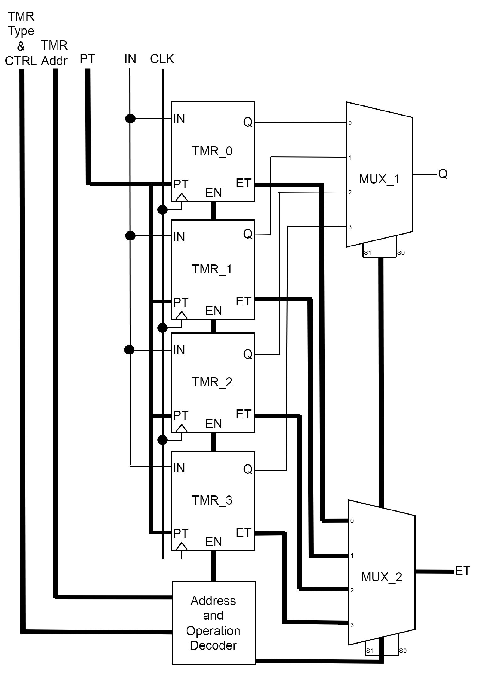
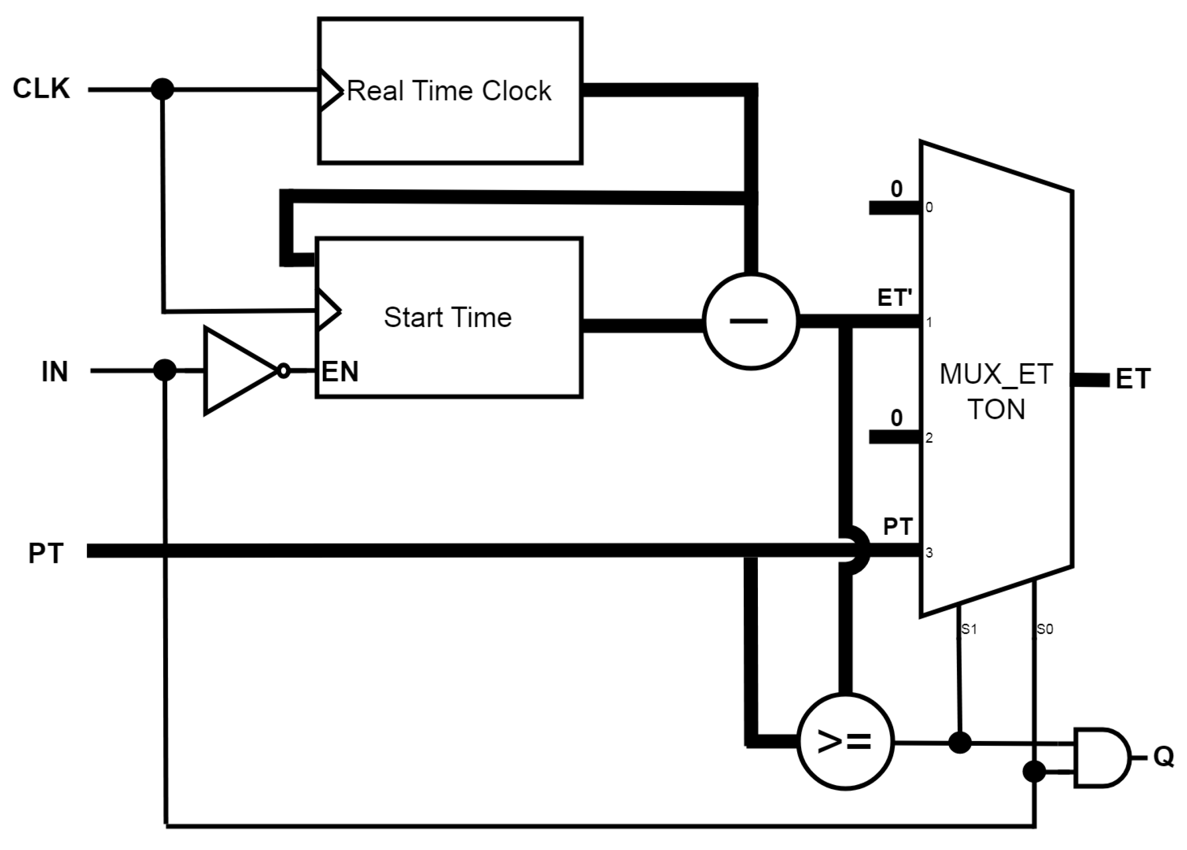
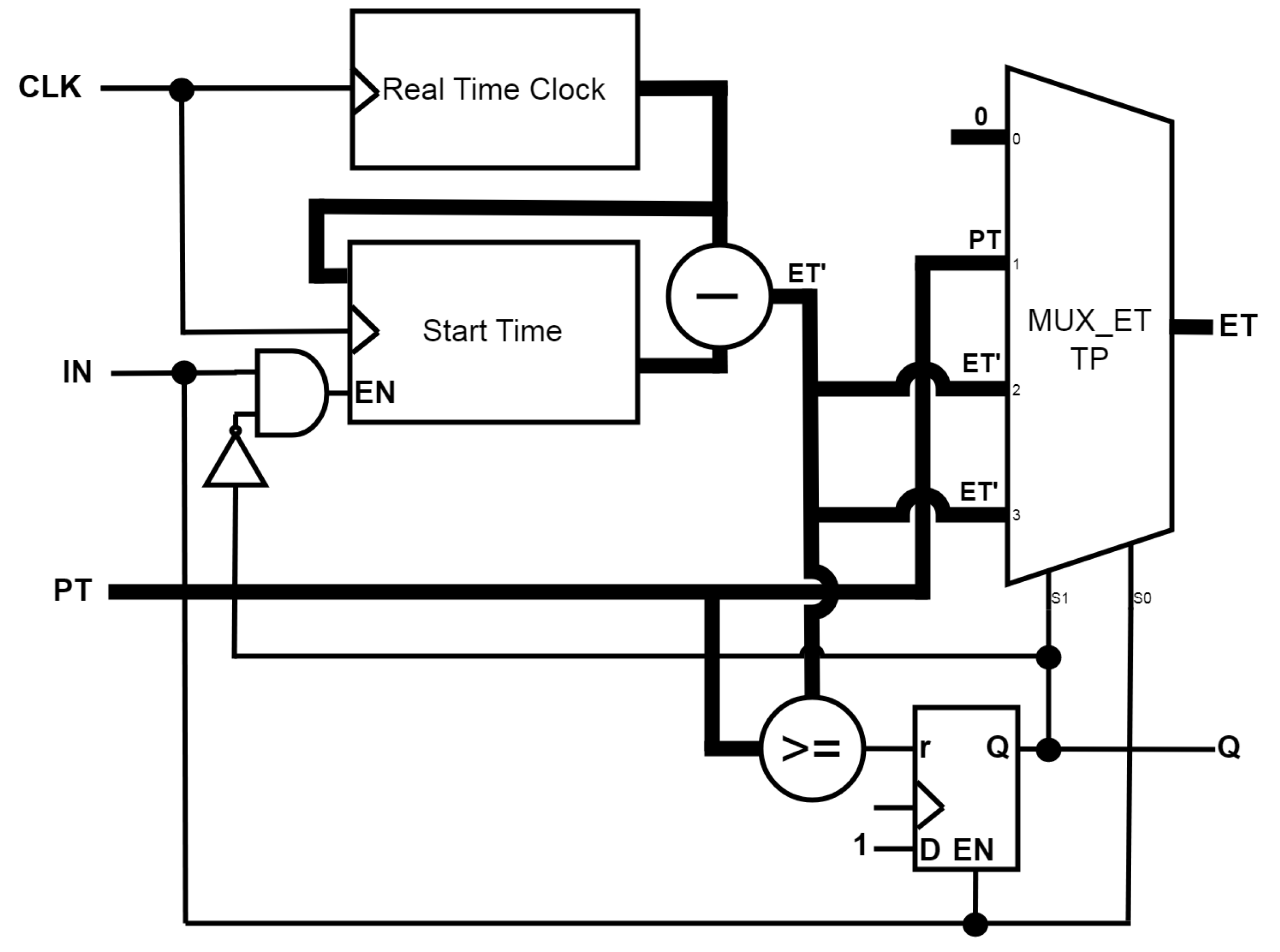
The main contribution of the paper is to propose a structure of the timer FBs for PLCs compliant with the IEC 61131-3 standard. All three designs are developed and presented, timer-on, timer-off, and timer-pulse, with each type designed to be fully hardware or software-like, and able to operate in multi-channel mode. The idea of a CPU architecture with hardware support is proposed. Finally, the paper presents the results of the implementation in an FPGA of the Kintex UltraScale+ family from AMD-Xilinx.
2. The Timer
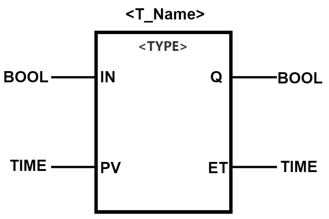
Figure 1 shows a graphical representation of the timer. The interface of such FB is defined by the following:
IN (input) [BOOL]—triggering input; the edge of this input initiates the time measurement;
PT (preset time) [TIME]—value for evaluation of the Q state;
Q [BOOL]—status of the timer;
ET (elapsed time) [TIME]—value of actual state of the timer;
<TYPE>—TON (time ON-delay time), TOF (time OFF-delay time), or TP (pulse timer) timer function;
<T_Name>—name of the timer instance.
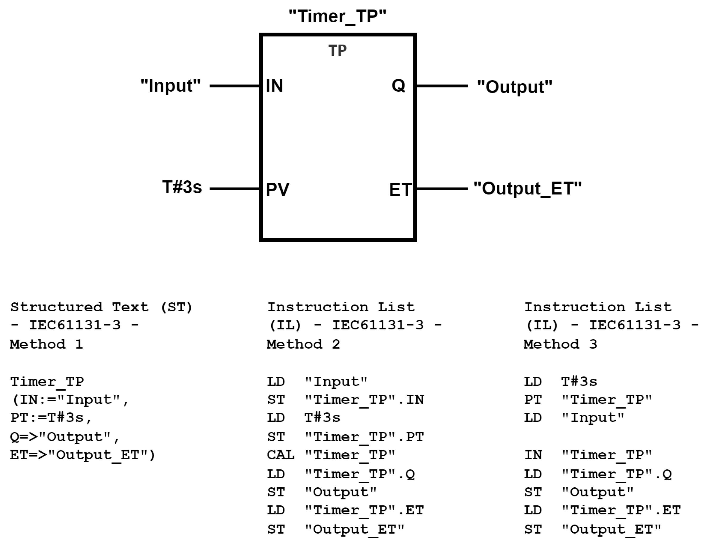
The declaration of the inputs and outputs of the timer TP function module within the Structured Text language is described in the standard [
1] and is shown in Listing 1.
| Listing 1. Declaration of the TP timer in Structured Text language. |
FUNCTION_BLOCK TP IN (BOOL) PT (TIME) Q (BOOL) ET TIME) VAR_INPUT IN : BOOL; PT : TIME; END_VAR VAR_OUTPUT Q : BOOL ; ET : TIME; END_VAR
|
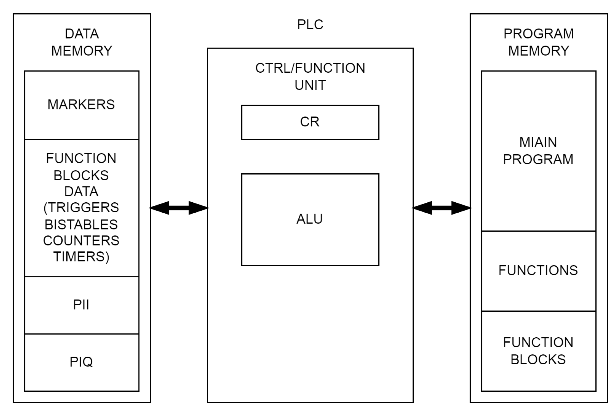
The implementation of timers needs mapping of a data structure in the PLC memory that store the current content of the timer ET, the status of the PT input and the status of Q output. However, Q and ET can be calculated at the moment of reading, so the data structure may not contain them. An additional memory cell may be necessary to store previous statuses of the IN (IN’). The actual set of memory cells associated with a timer is closely related to the implementation used in a particular PLC solution.
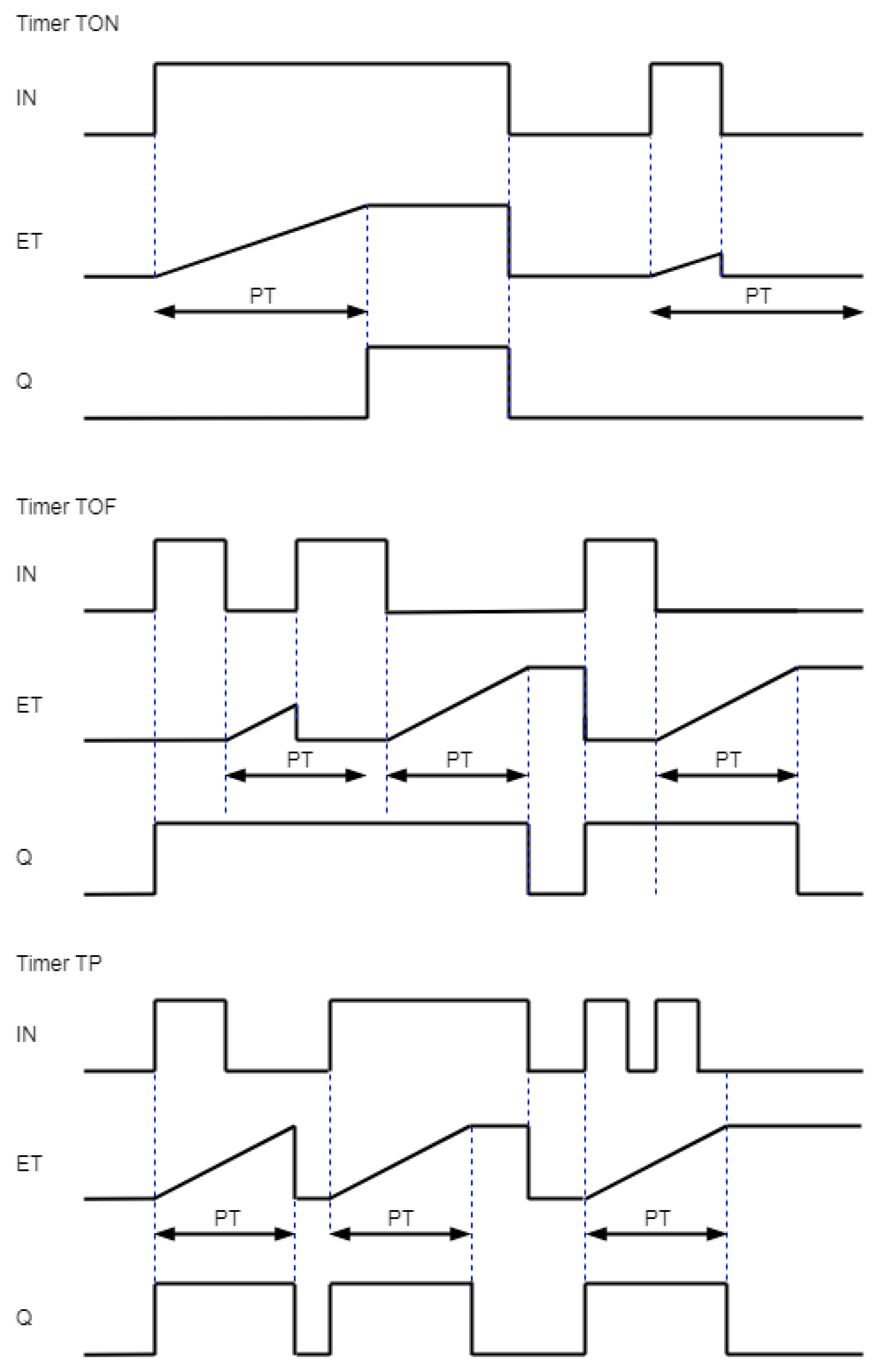
Any attempt to describe the work of the timers should, however, begin with an analysis of the time charts presented in
Figure 2.
The standard defines three types of timers:
TON—when IN is active, the timer counts time up, and after reaching PT, the binary output Q is activated. Output ET shows the actual time state of the timer.
TP—gives a pulse on the output after positive edge detection on the input.
TOF—when IN is becoming inactive, the timer counts time up, and after reaching PT, the binary output Q is deactivated.
Pseudo-code that explains the operation of the different types of timers is presented in Listing 2.
| Listing 2. Description of the timer presented in the standard. |
//Time On Delay TON IF !IN THEN ET := 0; ET_EN := IN ∗ (ET<PT); Q:=IN ∗ (ET>=PT) //Time OFF Delay TOF IF IN_FP THEN ET := 0; IF IN_FN THEN IN_INT := 1; IF IN_FP | (ET>=PT) THEN IN_INT := 0; ET_EN := IN_INT; Q := IN | INT_INT; //Pulse Time TP IF IN_FP THEN IN_INT := 1; IF !IN ∗ (ET>=PT) THEN IN_INT := 0; ET_EN := IN_INT ∗ (ET<=PT); IF !IN_INT THEN ET := 0; Q := ET_EN;
|
2.1. The Timer Operation
The description of timers in the standard is laconic. It mainly focuses on showing the time waveforms during their operation. In view of this, any designer of a PLC CPU will have to answer some basic questions:
- 1.
With what accuracy should timers measure time?
- 2.
What should be the range of measured time?
- 3.
How and where is the type of timer determined, that is, how does the timer measure time? To be more specific: when does the timekeeping process start, under what conditions does it continue, when does it end, and what is the generation of the binary output state of the timer Q?
- 4.
How and when does the controller store the state of the inputs/outputs in the context of each timer update?
- 5.
How and when does the timer inform the control program of changes in its structure, that is, when are the states of the timer memory cells modified (by which the program recognizes that something has changed in the timer)?
Regarding the first two questions, the standard suggests a solution. This is because it defines two types, TIME and LTIME:
TIME—the range of values and precision of presentation in these data types is implementer specific.
LTIME—the data time LTIME is a signed 64-bit integer with units of nanoseconds. The update accuracy of the values of this time format is implementer specific (i.e., the value is given in nanoseconds, but it may be updated every microsecond or millisecond).
The selection of values and precision can be determined using previous experience and what has been implemented in existing controllers on the market. From the analysis, it appears that most of the timers offered in commercially available controllers measure time with a resolution of 1 ms, and the range of this measurement is an integer, which is stored as 32 bits (the DINT format). This gives the possibility to measure 4.29 × 10⁹ ms, which is less than 50 days, which seems to be completely sufficient for most industrial facilities. In contrast, for the LTIME format, we obtain 18.45 × 10¹⁸ ns, which gives 213,504 days.
As for the type of a particular timer instance, it is assumed that this is defined in the declaration part of the program, but the standard is quite poor in the details. In graphical languages, there is an explicit designation of the timer type, which is not seen in textual languages.
Crucial to the implementation of the timer project is the answer to the last two questions. The answer is quite complex, and this topic is discussed in the next section.
2.2. The Call to the Function That Triggers the Timer
The standard defines three ways of calling timer operations in IL. The first is to call an FB with the parameters passed in parentheses [
1], as presented in Listing 3.
| Listing 3. The timer CAL. |
|
This type of call may not contain a complete list of assigned parameters but only the selected parameters. In such a case, the unassigned parameters take the values stored previously ([
1]: see Table 42 on page 105). This way of calling is available in Concept [
25] or CoDeSys [
26] software, as well as in the SIMATIC S7 IEC timers [
27].
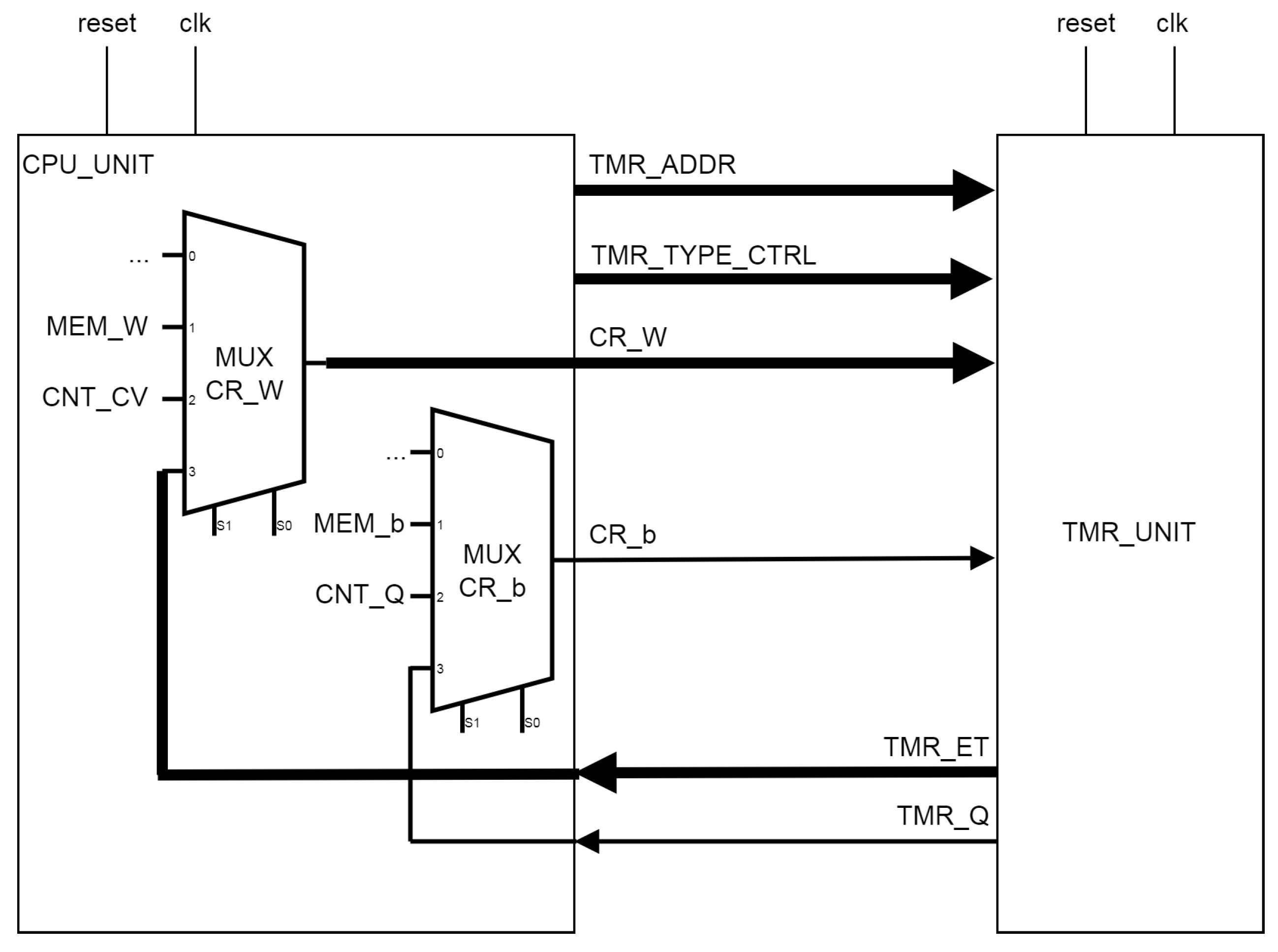
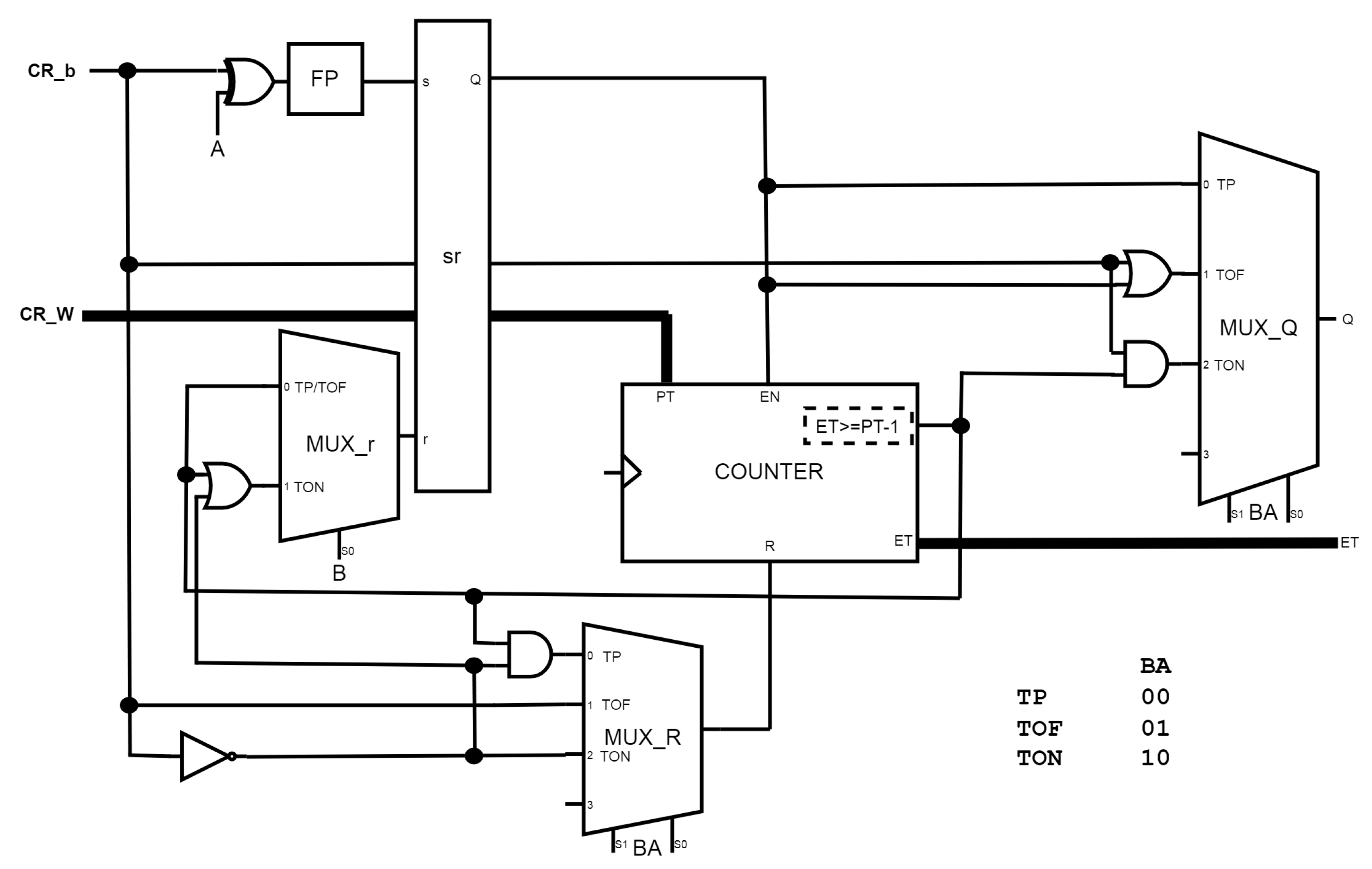
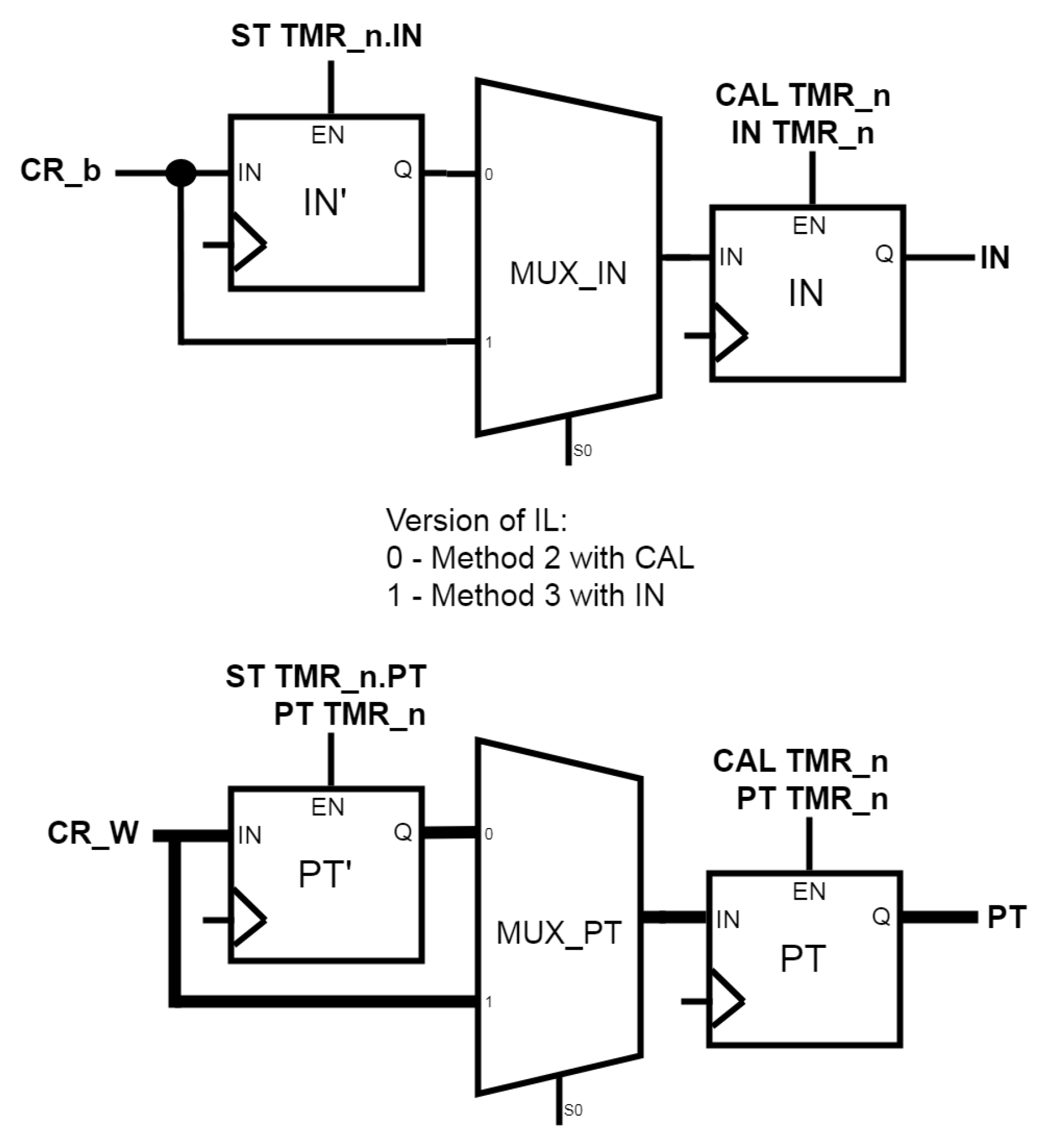
The second way consists of preparing suitable data in particular fields (using LD and ST instructions) of the timer structure and then calling the function, updating the timer without any parameters using the CAL command. If not all fields of the structure are assigned, the function uses the values of the structure fields stored earlier. As shown in Listing 4, there is a set of instructions (LD instruction) for loading data into the current result (CR) register and storing data to the individual fields that make up the timer structure (ST instruction). As opposed to counters, where functionality is realized only when the CAL instruction is executed, a timer counts the time units, so it must work all the time. Timer handling consists of two sets of actions: trigger handling (based on the IN-input state and the current timer state) and timer refreshing, which may or may not be performed as part of the CAL execution. There are four moments when the timer has to/may give new results—is refreshed:
This method is available in the Concept [
25], CoDeSys [
26], UnityPro [
28], PLCopen [
29], and ISaGRAF [
30] environments.
| Listing 4. Timer block calling using the CAL instruction. |
|
However, the provisions of the standard also allow the use of so-called short IL operators. The problem is how to refresh the timer while calling short operators IN and PT (
Figure 3). Regarding the short operators, the standard is somehow weak. Each short operand updates the timer state, so it improves the conciseness and program readability. But an analysis of the standard leads to the conclusion that each use of the short command is followed by CAL. This significantly affects the implementation of the timer block and has a big impact on the execution time of this block. In the Siemens SIMATIC S7-300/400 PLCs, the basic timers do not form an FB. Therefore, there is no problem using only timer elements that are necessary at that moment. It may seem that in this case the processing time of the timer is reduced. Among the implementations of the standard known to the authors, only Concept allows the use of operator-based programming. UnityPro, CoDeSys, and ISaGRAF do not allow this method of timer calling. An example code is presented in Listing 5. A program written using the short operators needs to be translated into short operators with an implicit CAL instruction. As a result, it takes longer to execute than a program explicitly using the CAL command.
| Listing 5. Timer block in IL using operators. |
LD IN_PT PT TMR ;Equivalent to: ST TMR.PT + CAL TMR LD INP IN TMR ;Equivalent to: ST TMR.IN + CAL TMR ;Operators take into account the current state of all bits in the TMR structure ;Explicit CAL not required
|
2.3. Ways to Measure Time
The concept of measuring time can have two meanings. The first meaning is the action of determining with satisfactory accuracy how long a certain event lasted. The result of such an action is a number expressed in units of time (usually seconds with a fractional part) giving the measured duration of the event. The second meaning of the concept of timing is to generate a binary sequence (pulse or delay) of a given duration. In this case, the control quantity is the number of time units, and the result is a waveform at a specific output in response to a so-called trigger event. Timers used in industrial automation systems realize timekeeping in the latter sense. However, it is also possible to use timers to determine the duration of an event occurring at a specific input, but this is not among their primary uses.
Ways to implement timers in PLCs include the following:
- 1.
Analog timers—these types of timers use integrated univibrators with an external resistor and capacitor circuit. The pulse duration is set in the hardware, using a potentiometer. This type of timer can be found in companies’ early industrial controller designs. The disadvantage of such a solution is the low accuracy and repeatability of the pulse length, as well as the inability to change the setting by program.
- 2.
Counter-based timers—the principle of operation is based on counting pulses of a reference frequency. The resolution of these timers is determined by the reference frequency. Virtually all timing systems encountered today belong to the group of counter timers. The systems differ significantly in the way they refresh (i.e., update the time value) in the timer register. The refreshing methods encountered can be divided as follows:
- (a)
Timers refreshed cyclically by the operating system of the controller. In this type of timer, refreshing occurs at every specified interval, such as using a cyclic interrupt. In each cycle, the state of all timers is refreshed regardless of whether they are used. This requires hardware support. The data structures for the timers usually occupy a specific place in memory, and there is a strictly defined number of them. The frequent refreshing of all timers takes a considerable amount of time, which can lead to a noticeable slowdown in the speed of the controller. To avoid slowing down the operation of the CPU, the timers refresh every 10 ms or less frequently, which leads to a lower resolution of timekeeping.
- (b)
Timers refreshed during the execution of a timer instruction. This method requires the timer instruction or timer-triggering function to be designed so that each time a program segment containing this instruction is executed, the timer state is refreshed. The advantage of such a solution is that the handling functions do not slow down the controller cycle (there are no cyclic interrupts designed to refresh all active timers). Also, the number of timers running in this way is not limited by hardware and depends only on the size of available memory. Triggering a timer operating on this principle involves rewriting the state of the system millisecond counter to the timer’s “Start” register. Refreshing involves subtracting the value stored in the “Start” register from the current value of the system millisecond counter and writing the difference to the ET register. This results in a rather significant disadvantage of this type of timer, which is the need to store as many as three numerical values: the initial value of “Start”, the preset value of PT, and the currently measured value of ET. In modern control systems, where memory capacities are much larger, this disadvantage has lost its importance.
- (c)
Timers refreshed every controller cycle. PLCs work in a serial-cyclic manner, that is, after each execution of the main block, operating system activities are carried out. These activities include rewriting the output image memory to physical outputs, rewriting the status of physical inputs to the input image memory, handling communication tasks, diagnostic functions, and so on. It is possible to include timer refresh activities in this phase of the controller cycle. This allows for a significant simplification of the activities performed by the program during the execution of the segment containing the timer instruction—it is only required to rewrite the state of the reference counter (millisecond counter) to the “Start” register of the timer. All other activities are handled systemically at the end of the cycle. The memory requirements of such a solution are similar to those of solution 2b, and the time outlay is greater and constant, because all timers are required to be refreshed after each cycle regardless of whether they are used in the program. The resolution of the timekeeping is limited by the cycle period of the controller, and this depends on the size of the program.
- (d)
Timers refreshed at the time of reading. This method of refreshing the timer is based on the observation that the state of the timer has no meaning until that state is checked. Thus, the refresh of the timer is performed immediately before reading its state in the form of a Q bit or ET value. The memory requirements for such a solution are identical to those of cases 2b and 2c. The complexity of the triggering instruction is analogous to case 2c. The advantage is the availability of the most recent Q and ET value at each reading, even if the reading is performed several times in a program cycle. The timing resolution does not depend on the program size and cycle time—it is always equal to the period of the reference counter (usually 1 ms).
Refreshing at the beginning of the cycle and during the execution of the CAL command means that the accuracy of the measured time reading is limited by the cycle time of the software loop. Asynchronous (system) refreshing and refreshing at the time of reading guarantees that the read time value is always up to date. Therefore, when designing a timer block operating in an FPGA chip, the (b) and (c) refresh methods were rejected.
5. Experimental Results
The software-like and hardware timers were implemented using Verilog HDL. Functional verification were run to search for bugs and to improve the designed constructions. The experimental results include two main comparisons:
A comparison of the logic utilization for software-like and hardware timers is presented in
Table 1 and
Table 2. The Xilinx Kintex UltraScale+ was used (xcku3p-ffva676-1-i). Synthesis was performed for different numbers of implemented timers: 16-1024 (address width: 4-bit to 10-bit).
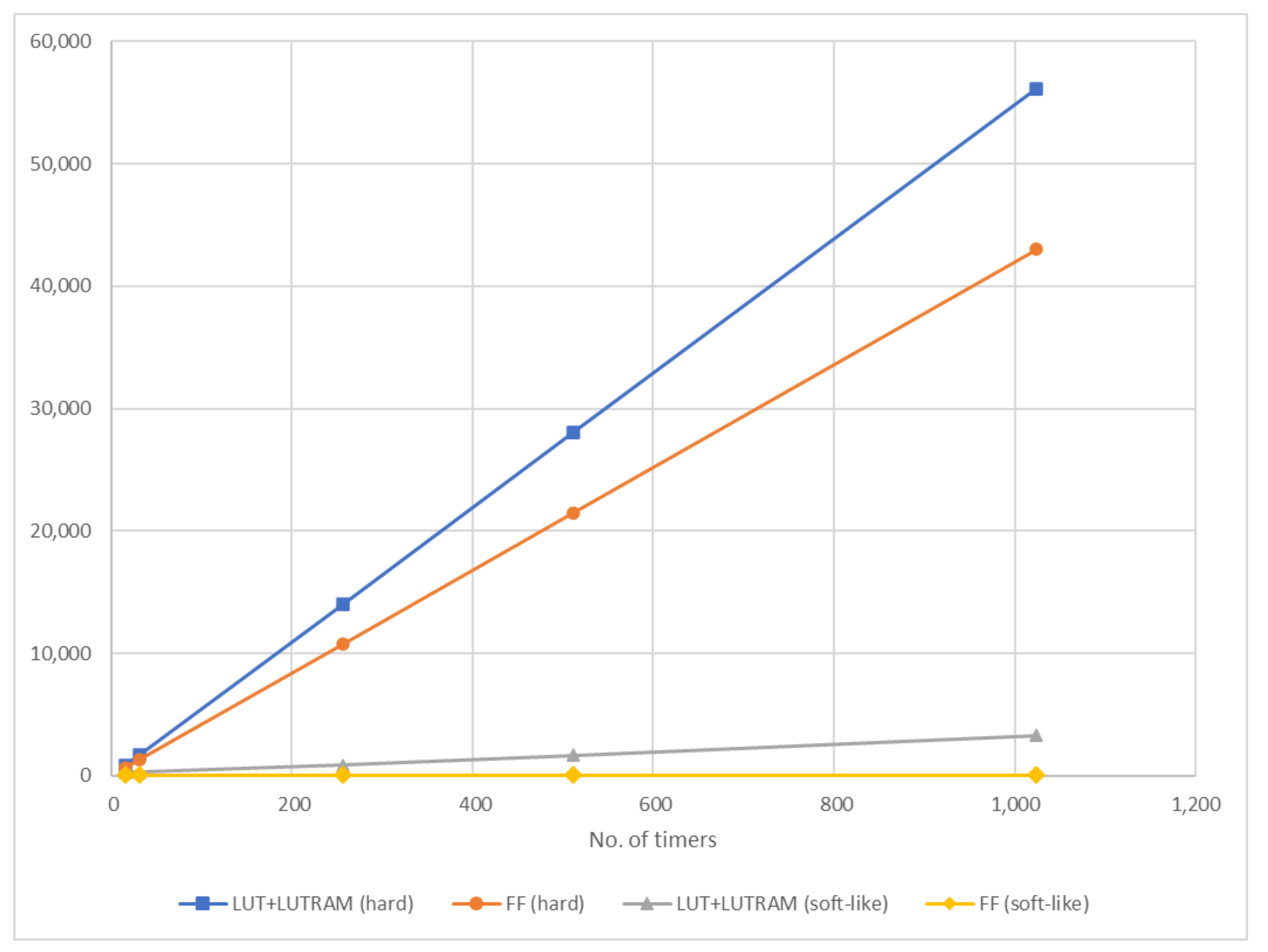
A direct comparison of the logic utilization for software-like and hardware timers is presented in
Table 1 and
Figure 16. The number of look-up tables (LUTs) used by the timers increases linearly with the number of timers, whereby hardware timers utilize only simple LUTs, and software-like timers utilize LUTs and LUTRAMs, which are consumed for memory construction. Note that the amount of resources consumed grows much faster for hardware timers than for software-like timers. In addition, hardware timers also consume flip-flops in their design, whereas the number of flip-flops in a software-like solution is constant.
Table 1 shows one deviation from the linear increase in the LUTRAMs used. For software-like timers, 16 and 32 timers use the same resources. This is because the LUTRAMs in the FPGA family are 6-input LUTRAMs, which means that for fewer than 32 timers, the LUTRAMs are used inefficiently.
Figure 16 shows the sum of LUT and LUTRAM resources due to the similar logical purpose of these blocks for building digital circuits. This makes it possible to make a close and direct comparison between the solutions.
To fully compare software-like timers with hardware ones, a timing analysis was performed. The developed timer units were implemented in a simple CPU. The purpose of this experiment was to compare the consumed resources and the maximum frequency of the timer network in a fully functional unit. The idea is to implement CR_b and CR_W accumulators along with all multiplexers and memories (e.g., PII and PIQ) to enable the timer tasks. Such a comparison, first of all, gives a proper overview of the speed of the different types of timer blocks. The results of the implementation (resource utilization and maximum frequency) are shown in
Table 2, whereas the comparison of the maximum frequency (in MHz) of the obtained units is shown in
Figure 17.
Most significant in this comparison is the obtained maximum clock signal frequency—. It is clear that the pure hardware solution is faster and yields frequencies of 282–302 MHz, whereas the analogous software-like solution yields frequencies of 225–251 MHz, which is about 17% lower compared to the hardware solution.
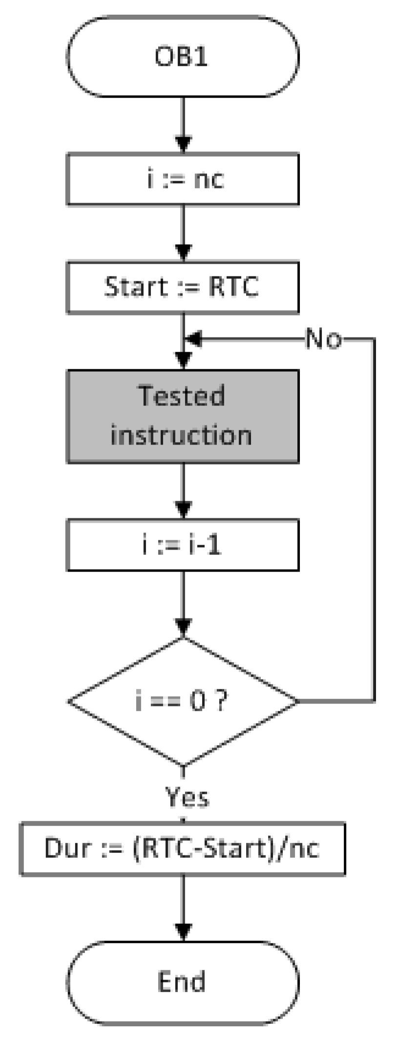
The results of the developed implementations were compared with the measurement results obtained for Siemens PLCs. An iterative algorithm was used to measure the execution time of timer commands, which was the basis for their comparison. The block diagram is shown in
Figure 18. Before starting the next iteration, the current time is stored in the Start variable. For the assumed number of iterations (nc), the same measured instruction is called cyclically. At the end of the cycle, the instruction execution time is determined by the difference of the start and end times of the iterative process divided by the number of iterations. This method of measuring the instruction execution time is subject to error due to the iterative process itself, so in order to perform the calibration, the instruction under test was first removed from the program and the execution time of an empty program was measured. The actual instruction execution time was taken as the difference of the time obtained for the program containing the tested instruction minus the execution time of the empty program. To reliably determine the timing of the program, 100 measurements specified by the algorithm were taken. Coarse errors, such as those related to the operation of the operating system, were removed.
A comparison of the time required to process all the timer operations (Listing 4) was made. The execution of each instruction requires exactly one clock cycle for presented CPU. The comparison was made with Siemens solutions—
Table 3. The table shows the measured processing time for the program using all capabilities of the timer. For the controller S7-319 3PN/DP, there is huge disproportion between the implementation of the timer operations as a whole for the classical and the standard compliant solutions (
Table 4). The structure proposed in the paper significantly exceeds the time performance of all other compared units. For example, in the S7-315 controller, the simple operation (
A M x.y) takes almost nine times less than the state of the timer read instruction, and these operations for the S7-319 take almost four times more time to execute. Therefore, the execution times of individual timer tasks were compared with respect to the duration of the instruction that was assumed to be basic in every CPU controller: the instruction for reading the status of the contents of the PLC memory cell M (marker, memory). Thanks to this, it is clear that the implementation of timer operations proposed by the authors is much more time efficient than the implementation in Siemens PLCs, regardless of whether timers are 16-bit or 32-bit or whether the timers are the classic version (not compliant with the provisions of the standard) or the version compliant with the standard (most closely to short operators). In the best case, for the S7-315 controller and the timer not conforming to the standard, the difference reaches more than 10 times, whereas for the timer conforming to the standard and the S7-1516 controller, the difference is more than three times. The best result gives S7-319 3PN/DP for the non-standard solution of the timer—this CPU is only a little more than two times worse than the authors’ solution. A very interesting example is the comparison of the execution time of the instruction for reading the binary state of the timer (output Q) with that for reading the bit state of the marker. For the presented controller, this quotient is, of course, 1, and the best result for the SIMATIC controllers is almost 2.5, a classic timer, and almost 4 (S7-319 3PN/DP), a timer compliant with the standard, and the worst is 19.25 (S7-1214). These differences are due to the fact that the timer operations for the proposed units, due to the hardware support, are implemented concurrently and take the same number of clock periods as the basic instructions (such as reading or writing a memory cell).
6. Conclusions
The design of timer FBs compliant with the IEC 61131-3 standard is proposed in the article. Four types are presented: TON, TOF, TP, and universal. Each type is designed to be fully hardware or software-like. The multi-channel structure is provided.
It is noteworthy that the software-like design is implemented without edge detectors. Such a feature is obtained by reversing the method of time determination by counting the difference between the start and end times and by using specific features of the D flip-flops, that is, clock-enable inputs.
Thanks to the universal design and minimalistic interface, the proposed FBs can be used for hardware support of off-the-shelf units or be integrated into newly built PLC CPUs. The presented timers may be implemented using in FPGAs as well as integrated with the CPU in the form of presented in the paper bit.WORD integrated hardware–software PLC. The paper focuses on the solution of the CPU, which implements the control program in the classical way (i.e., serial–cyclic). The timers themselves are built-in hardware. The task of the program is only to control them appropriately. Therefore, the operation of the timer algorithm itself is entrusted to hardware and is done concurrently to main tasks performed by the CPU.
The presented timers solutions are described in Verilog HDL. They are implemented in an FPGAs with a dedicated software core microprocessor. The paper presents the results of the implementation in an FPGA of the Kintex UltraScale+ family from AMD-Xilinx. Both the classical hardware timer built on the basis of flip-flops and software-like are hardware-based solutions. Software-like timers are based on memory cells on which operations are performed. Both structures are very fast and make it possible to execute the timer update operation in a single clock cycle. However, hardware timers provide faster structures, and they utilize flip-flops, while software-like timers are slower designs but are based on memory-dedicated FPGA structures. The results of the implementation in an FPGA are reported and prove the high efficiency of the proposed solution.


