1. Introduction
In simple electronics experiments, it may be the most cost-effective to obtain data using common measurement devices, such as multimeters, oscilloscopes, oscillographs, strip-chart recorders, compact data loggers, or interconnected standalone instruments. As the experiments or measurement functions get more complex or demand extensive data manipulation, a data acquisition system (DAQ) is often a better choice [
1].
Data acquisition is the process by which physical phenomena from the real world are transformed into electrical signals that are measured and converted into a digital format for processing, analysis, and storage by a computer. In a large majority of applications, the data acquisition (DAQ) system is designed not only to acquire data but to act on it as well. In defining DAQ systems, it is, therefore, useful to extend this definition to include the control aspects of the total system [
2]. A DAQ system is comprised of a computer running specialized software and several data acquisition cards and/or instruments (from now on jointly referred to as DAQ devices). Data acquisition (DAQ) systems are intensively used in laboratory research, industrial facilities, aviation, automotive, etc. The applications include test and measurement, automation, etc. [
3].
One important consideration when designing a DAQ system is the total system throughput in bits per second. When considering a single channel, the parameter translates to maximum throughput per channel (in bits per second), which, if all the channels are of the same type, equals the total system throughput divided by the number of channels. Since the useful information is stored in binary samples and not in single bits, the equivalent acquisition rate of a channel (in samples of a given width per second) could be obtained by dividing the maximum throughput per channel, diminished by possible protocol overhead, by sample bit-width. Please note that, in this paper, we reserve the term sampling rate to times when referring to analog-to-digital (ADC) and digital-to-analog (DAC) converters.
In general, a DAQ device operates in up to three signal domains (analog, digital, and temporal) and up to two signal directions (input and output).
There are four limiting factors for the acquisition rate of a DAQ system: conversion time, DAQ device processing time, communication time, and host processing time.
Conversion time is the time needed for the data to propagate from the outside world to the inside of the DAQ device. The time may be relatively long, as in the case of analog inputs and outputs, where it is defined by sampling rates of ADCs and DACs, respectively. The other extreme is the case of digital inputs and outputs, where the time is very short, defined by delays of digital logic only.
DAQ device processing time refers to the time needed for the interpretation of data received from and formatting of data to be transmitted to a host, notably if data aggregation is utilized. This time also includes device-local processing of digital data samples if available.
Communication time depends on the employed communication technology. Apart from the communication interface speed, the maximum message size and message data overhead also contribute to the parameter.
Host processing time in the case of input signal direction relates to the time needed at the host computer for reception and interpretation of data, which can be followed by analysis, visualization, storage, or further transmission. In the case of output signal direction, the parameter relates to the time needed for the acquisition of samples from a graphic user interface, control algorithm within the application, local storage, or over a network, their formatting, and transmission. This parameter is longer for the former case due to the higher amount of processing involved.
From the above exposition, it is obvious that the acquisition rate is critical in the case of analog input signals, and that is the focus of this paper. Analog input signals originate from various devices, such as sensors, that is, non-electric to electric transducers. DAQ systems with analog inputs find their application in scientific experiments, industrial applications, medical diagnostics, agriculture, civil engineering, energy plants, wireless sensor networks, space exploration, etc.
The parameters used to describe the analog input portion of a DAQ system are the number of sampling channels and resolution and maximum sampling rate of the ADC used within a DAQ device [
1]. Depending on the application and desired capabilities of the DAQ system, characteristics of input signal conditioning, i.e., signal filtering and amplification, should be reviewed as well. Other characteristics common to the entire DAQ system include the type of permanent data storage on the host device and the type of interface used to communicate with the host. Visualization and advanced processing of the captured data on the host device can be important as they enhance their utilization.
As pointed above, the acquisition rate of the analog input DAQ (sub)system depends on the ADC sampling rate, the processing speed of the DAQ device, the transfer rate between the DAQ device and the host device, and the processing speed of the host device, dependent on the actual data manipulation at the host.
Commercially available solutions and some of the solutions presented in the scientific literature for data acquisition applications come in the form of oscilloscopes, advanced data loggers, logic analyzers, and other specialized tools, usually based on plug-in DAQ boards [
3]. These general-purpose DAQ instruments are well suited for measuring voltage, current signals, or resistance, and they can include some form of signal conditioning. The main drawback of such systems is that they are expensive, or cumbersome, or both [
4,
5].
Another issue arises when there is a need for remote data acquisition. Various long-range communication technologies may be used, wired or wireless, or a combination of the two. The features of concern when selecting appropriate technology are range, transfer speed, and cost. Power consumption may also be addressed, but if a high acquisition rate is desired, there is little room for power savings.
There is a growing demand for real-time acquisition of analog signals with high-frequency content (wireless communications, space applications, particle physics experiments, etc.). The signal’s source is frequently far away from the location where data are collected for processing. Another requirement is to keep the total system cost as low as possible. Therefore, there is a need for affordable and reliable remote analog DAQ systems capable of accurate representations of fast signals.
In this work, we developed a method for designing such a system based on a microcontroller platform. We focus on a single channel case, but our results should easily scale to any number of channels with an inevitable decrease in maximum throughput per channel. A high ADC converter sampling rate is inherently necessary due to the Nyquist theorem [
2], and there is consequently the need for high-speed communication technology so that a significant amount of data can be reliably transferred. Since the data path within the system consists of sequentially connected functional blocks, the acquisition rate cannot exceed the processing rate of the slowest block. To optimally utilize the various functional blocks and maximize the acquisition rate, it is necessary to implement efficient synchronization of data transfer between them. Our design method maximizes the performance of a data acquisition system using state-of-the-art, high-end, yet affordable hardware and getting maximum performance through the utilization of an efficient software architecture.
Although it is possible to write microcontroller firmware that is very efficient, the ever-increasing complexity of modern microcontrollers makes writing efficient firmware difficult and time-consuming. For that reason, the utilization of a real-time operating system (RTOS) becomes beneficial, if not a must. Therefore, our method uses a microcontroller, with an integrated or connected to an external ADC, running an RTOS. This way, application firmware can efficiently manage the process of converting analog measurement data and sending these data to a remote PC, which is used there for real-time visualization, analysis, advanced processing, and storing of collected data.
The aim of our design method is to exceed the accuracy, speed, and ease of use of existing solutions but also to allow a user the freedom to adjust the system to specific needs. In order to demonstrate the proposed methodology, we provide an example of such a system using a Cortex-M7-based 32-bit microcontroller [
6] with integrated ADC and Ethernet MAC interface [
7], FreeRTOS real-time operating system [
8], and an efficient, user-friendly PC application written in Qt [
9] for visualization of the collected data and its FFT.
Methods related to the utilization of hardware capacity and operating system supporting real-time concepts are well-known independently. However, the selected model of interaction between hardware and software, in the form of hardware-software codesign, is provided by the software architecture. That way, the entire platform hardware capacity is utilized in an optimal way with a minimum latency. Consequently, there are concurrency and parallelism at sampling, processing, and data transfer levels.
The main paper contributions are:
MCU-adapted two-stage pipelined dataflow approach, which, in combination with hardware and software optimization techniques, achieves maximum hardware utilization. The abovementioned techniques incorporate the utilization of high-speed on-chip memories, DMA controller in combination with Fast ADC, and Ethernet controller with dedicated DMA.
DAQ device firmware architecture that adopts RTOS-driven concurrent programming model in order to achieve a dual channel data stream and control flow. A low processing latency is achieved by utilization of the approach based on synchronous event processing.
Architecture for host machine application based on a concurrent programming model that achieves real-time visualization and processing of data samples, as well as monitoring of the quality of data transfer service.
The general-purpose acquisition system software architectures applicable to any high-speed sensing or metering systems based on an MCU and a host computer.
A low-cost remote DAQ system solution consisting of a DAQ device (based on off-the-shelf MCU development platform with Ethernet capability [
10]), and a software tool for real-time visualization, analysis, and logging of data samples. The solution outperforms the existing works in terms of completeness of functionalities and achievement of maximum, platform-limited sampling rate.
The remainder of this paper is organized as follows.
Section 2 presents the related works in the field of high-speed DAQ systems. Theoretical considerations of designing a data acquisition system are conducted in
Section 3.
Section 4 proposes the software architectures of a high-performance remote DAQ system. The practical implementation of a high-performance remote DAQ system is outlined in
Section 5.
Section 6 presents the experimental results of a laboratory prototype. Concluding remarks, architecture limitations, and the directions for future work are given in
Section 7.
2. Related Work on Fast DAQ Systems
In this section, we provide a survey on fast DAQ systems. However, any survey of existing DAQ systems cannot be exhaustive since DAQ systems are usually custom-made and they rely on too different requirements.
We focus on relatively recent works only. Moreover, we do not consider commercially available DAQ systems and, because the focus of this paper is the research of design methods of entire DAQ systems, we do not include papers that employ commercial plug-in DAQ devices within the system.
A DAQ system can have either a relatively slow or a relatively fast data transmission speed; it can store and display collected data locally on the main DAQ board, or it can send data to be stored and observed remotely; it can have its own ADC or just collect sampled data from an external ADC; etc. The flexible definition of a DAQ system allows many different types of systems to be classified as DAQ systems. This can make researching and comparing different systems a challenging task, and it can make research results hard to interpret. Since the aim of the paper is the development of a fast DAQ system, we present some fast DAQ systems from the literature, and because fast and slow are relative terms, in this paper, we consider all DAQ systems with sampling rates over 1 kSps to be fast systems.
Although the DAQ system design method presented in this paper utilizes microcontrollers for achieving high acquisition rates, we review FPGA-based systems as well because the same main functional system components can be observed in both cases. Therefore, for the sake of a better overview, we sort the related works into two system groups: FPGA-based and microcontroller-based DAQ systems.
2.1. FPGA-Based Fast DAQ Systems
The main reasons FPGAs are used for designing DAQ solutions is their ability to operate at very high clock frequencies with the possibility of parallel processing, in turn, enabling fast processing of acquired data. Power can be conserved on FPGAs by instantiating only hardware components that are necessary for a specific application. The potential for an increase in performance comes at the cost of a higher price, lower portability, and more complicated reprogramming when compared to microcontroller-based solutions. It is for these reasons that some FPGA-based DAQ systems are used for very specialized applications.
A DAQ system with fast processing and transfer speeds in mind has been designed in [
11]. The design of a high-speed FPGA-based DAQ system consists of an ADC with a 16-bit resolution for data conversion, two smaller-sized buffers used to store the temporary data samples, and a DMA that was programmed to achieve data transfers without loss of a single data sample when transferring sampled data from the temporary buffers assigned to the ADC to the DD3 SDRAM which is used as permanent storage. On the FPGA, a soft processor core was instantiated and tasked with initiating new DMA transfers. By overcoming the problems caused by the mismatch of operating frequencies between DMA, ADC, and SDRAM, the authors achieved a maximum acquisition rate of 10 MSps. The downside of such a design is the use of on-board memory as permanent storage, which makes it harder to utilize a PC to visualize and further analyze the acquired data, thus without the possibility to analyze the data in real-time.
Designing a highly specialized FPGA-based DAQ system was the approach taken in [
12]. This design presents a multichannel, high-speed DAQ system that supports acquisition for long periods of time, all of which are requirements of the Experimental Advanced Superconducting Tokamak (EAST) device [
13]. In the design, four ADCs are connected to an FPGA, which is then connected to a data server through a Peripheral Component Interconnect (PCI) Express interface. This allows acquisition from multiple channels synchronously with the acquisition rate of 80 MSps (20 MSps per channel) and the precision of 12 bits, with the acquisition lasting more than 1250 s of continuous sampling. Synchronous sampling of the four ADCs was achieved by instantiating a clock configuration circuit on the FPGA, which provides four phase-shifted clock signals. To extend the maximum continuous acquisition time, the authors have implemented the Lempel-Ziv-Oberhumer (LZO) algorithm [
14] on the FPGA, which allows for fast compression and decompression. By employing FPGA parallel processing mechanisms, data acquisition efficiency was not affected by compression. Even though this DAQ system was developed for a specific use case, data visualization could be improved because the paper features only a digital waveform view of the captured data in an unmentioned software tool.
A similar approach was taken in [
15], a design of a DAQ system developed for Superheated Emulsion Detectors (SEDs) [
16]. The paper presents a 10-channel, 12-bit resolution high-speed DAQ system with acquisition rates of 500 kSps per channel. The design features triggered acquisition and a user-programmable threshold with pre- and post-trigger adjustments. This allows the user to choose how many samples before and how many samples after the automatic or manual trigger are desired to be captured. Because of the specific application of this DAQ system, all 10 channels need to be sampled at once. Each of the 10 analog signals is connected to a signal conditioning board, followed by an ADC board, which is then connected to the main FPGA board, which features the main processor. All the 10 ADCs use the same sampling clock, and all the conversion results are read at the same time, stored in a circular buffer, and the converted values are compared with a threshold value. If the threshold value is exceeded, a configured number of samples before and after the threshold sample are collected and sent to a PC using a Universal Asynchronous Receiver/Transmitter (UART) interface [
17]. The DAQ system uses a graphical user interface (GUI) designed in LabVIEW [
18] to provide visualization of the collected data. Although the maximum possible acquisition rate simultaneously over all the channels is 5 MSps, UART communication technology does not allow for a higher baud rate than 921,600 bps, limiting the total system throughput when acquiring signals over longer periods of time. As soon as the internal FPGA buffers get filled, acquisition stops until all the samples are transmitted.
2.2. Microcontroller-Based Fast DAQ Systems
When a DAQ system is developed for a general-purpose application, microcontroller-based DAQ systems are generally a better choice. If needed, microcontroller-based DAQ systems are more easily adapted to a specific application thanks to easier reprogramming and changes in existing software. If a system is designed with portability in mind, it can be relatively easy to adapt the design from one microcontroller platform to another. The availability of different microcontrollers and the fact that more developers are better acquainted with microcontroller programming than FPGA programming also greatly increases the popularity of microcontroller-based DAQ systems over FPGA-based systems. Microcontrollers have grown into powerful yet complicated systems, but the utilization of an RTOS facilitates programming without wasting too much theoretical efficiency. This way, microcontrollers can even emulate the parallelism of FPGA.
A DAQ system used for high-speed current sensing is described in [
19]. The main purpose of this system is to detect faults during welding and mark damaged joints by comparing the recorded data to a learned pattern. The system consists of a sensor board that measures welding voltage and current waveforms with additional sensors and evaluation software running on a remote PC. The sensor board consists of a measurement part and a processing part that includes ADCs, a microcontroller, external memory and an Ethernet PHY module. A whole welding sequence can be buffered locally on the board. The board uses two 16-bit ADCs connected via SPI bus to the microcontroller. The sampling rate is 82 kSps, with averaging done in firmware, so the effective acquisition rate is 1 kSps. In order to run an open-source TCP server on the board, a Cortex-M7-based 32-bit microcontroller [
6] uses the Keil RTX RTOS [
20]. On the PC side, a MATLAB [
21] environment (version 9.5 R2018a) is set up to evaluate faults during welding. From the paper it is not clear, but it seems that the firmware is not divided into smaller tasks but uses just a main loop with interrupts.
To detect early failures in machinery equipment, a DAQ system for acquiring vibration signals in the X, Y, and Z axes in rotating machinery has been developed [
22]. The goal of the paper was to create a real-time, multi-parameter, high-precision, miniaturized, and portable DAQ system. The central part of the system’s hardware is a Cortex-M3-based 32-bit microcontroller [
23] with the μC/OS-II RTOS [
24] used to meet the multitasking requirements. To increase the portability of the system, an on-chip SRAM module is used for data storage, and an LCD touchscreen is used to display the acquisition results in real-time. A 12-bit ADC is used for sampling. The system can sample vibration signals from a selected axis at a time by sampling one of the three vibration acceleration transducers with a sampling frequency of 5 kSps. The firmware is divided into six tasks used for data acquisition, data transmission, data display, touch screen driver, key-press management, and μC/GUI interface [
25] for the touchscreen LCD. Data acquisition starts when an acquisition request is received and sent by the user. Acquired data are moved using a DMA and stored in the SRAM until it is full, at which point an interrupt signal is sent to the CPU, which stops acquisition, reads the SRAM, and displays the result on the LCD display. It is debatable whether this system, which collects data only on the user’s request and only until the storage is full, is really a real-time system. A software architecture diagram in the paper mentions a data transmission block that can communicate through USB, USART, and Ethernet, but it does not mention if, how, and when this block is used. Although increasing portability, storing data only locally and observation only using the LCD display greatly limits visualization and disables automated data analysis.
Xnode, a wireless high-fidelity DAQ system for structural health monitoring, has been presented in [
5,
26], developed with technical standards in China and lessons learned from previously developed similar systems in mind. The hardware of Xnode consists of three printed circuit boards—a processor board, a radio/power board, and a sensor board. The hardware is designed around a Cortex-M4-based 32-bit microcontroller [
27]. The system uses an external NAND flash memory for temporary and an SD card for permanent local storage but also features a wireless transceiver on the radio/power board for communication with a remote station, compatible with the ZigBee protocol [
28]. The sensor board features accelerometers and temperature sensors and an 8-channel 24-bit ADC with a sampling rate of up to 16 kSps and programmable antialiasing filters. The software is developed using FreeRTOS and a middleware service-oriented framework that supports network and application scalability. The application, which utilizes the middleware services, is organized into three tasks—application task, sensing task, and a radio task. The papers do not specify any visualization software that is used with Xnode, the lack of which can complicate the usage for users that are not experienced in that field.
OpenDAQ, a data acquisition and control system, was designed to be a cost-effective, multifunction computer-based DAQ system open to users [
29]. OpenDAQ has up to 8 analog input channels, a 16-bit resolution with a maximum sampling rate of 20 kSps for a single channel at a time, as well as one analog output. The system also has the option for digital sampling and control using the provided digital ports. The OpenDAQ hardware principally consists of an analog input signal conditioning block, analog output conditioning block, ADC, and an 8-bit AVR ATmega microcontroller [
30]. Microcontroller software does not utilize an operating system, and it is written using libraries, such as Arduino libraries [
31]. The system uses a USB connector for communication with a PC, which runs visualization and control software. The authors of OpenDAQ have created two options for the final user to choose from. The user can use either Python [
32] or LabVIEW [
18] for visualization and control. The wide range of capabilities and options the system offers makes it suitable for both industrial and educational applications. While OpenDAQ features an open design, it is possible that performances can be increased by the use of an RTOS. That way, the maximum acquisition rate could be increased to utilize the maximum 100 kSps sampling rate of the microcontroller’s ADC.
An example of a DAQ system used in the automotive industry can be found in [
33]. Like OpenDAQ, this system has been developed with cost-effectiveness in mind and utilizes low-cost components. The system is Arduino-based [
31], and the hardware has been developed as an Arduino shield. One of the reasons for this design choice is that the system is designed to be easily programmable and customizable for different uses in-vehicle data acquisition and control. Arduino Due [
34] is used as the development board because of the higher processing capabilities, the larger number of available inputs and outputs, and a higher resolution (12-bit) ADC when compared to other Arduino development boards. The result is a system that can acquire data from up to 12 analog inputs, an I2C sensor, an SPI sensor, and a GPS module along with multiple digital I/O pins. For applications where analog control is needed, there are two analog outputs. The maximum sampling frequency is 2 kSps if only one channel is used. Data can be stored locally using an SD card, or they can be stored remotely using Arduino’s serial communication. The shield uses a Bluetooth module to enable acquisition from a mobile device and an LCD for displaying the DAQ status. No visualization software has been developed for the DAQ system. Although the system offers a user the possibility to connect and sample multiple analog and digital sensors at once, the sampling rate drops significantly with every additional sensor connected, and it might be too low for some applications.
Papers [
35,
36] offer insight into another field where microcontroller-based DAQ systems find their use. In these papers, DAQ systems are used to acquire electrophysiological signals from live laboratory test animal subjects and send those results remotely. By using the UDP internet protocol, these systems achieve high data transfer speeds. In [
35], 16 analog channels with a 16-bit resolution are sampled using an external ADC connected to an ESP32-based development board [
37], which has a dual-core LX6 microcontroller [
38] and WiFi communication capabilities. Utilizing FreeRTOS [
8], the system divides tasks between the two processor cores to boost the performance of the system. This way, a total system throughput of 6.4 Mbps is achieved when acquiring 16 analog input channels simultaneously, with 25 kSps acquisition rate. The samples are wirelessly sent to the host using WiFi and, as mentioned previously, UDP transfer protocol. In [
36], the authors explore the advantages of using UDP protocol over TCP protocol to reach high data transfer speeds when using Ethernet communication technology. In the experiment performed in this paper, the maximum system throughput achieved using TCP protocol was 17.8 Mbps. When the protocol was changed to UDP, the maximum system throughput reached 47 Mbps when acquiring data simultaneously from 64 channels, with an acquisition rate of 24 kSps. Even though both systems are tailored for a specific, in-house application, visualization of the data acquired could be improved, which would increase the applicability of both solutions.
From the examples above, it becomes clear that to meet the requirements of high-speed, high-resolution acquisition using a microcontroller-based system, an RTOS is almost always needed. Although OpenDAQ manages to reach the maximum acquisition rate of 20 kSps for 16-bit resolution without an RTOS, any major increase in acquisition rate would require it. As seen in many of the papers mentioned in this section, an RTOS enables the system to divide microcontroller firmware into multiple tasks that can control sensing and communication with the outside world separately and concurrently. In order to increase the system’s applicability, it is beneficial to observe the collected data on a host system. For that purpose, it is necessary that the DAQ device has remote communication capabilities, and if high throughput is required, communication technology that supports high data transfer speeds is needed. With that in mind, it is advantageous to use high-speed protocols, for example, UDP, as shown in [
35,
36].
2.3. Comparison of the Reviewed DAQ Systems
Table 1 gives an overview and comparison of the DAQ systems reviewed in this section. The systems are compared in multiple categories that are essential when describing and choosing a DAQ system. The categories are as follows:
Number of channels—the maximum number of analog channels that can be sampled using the maximum acquisition rate,
Resolution—resolution of the system’s ADC,
System throughput—as defined in
Section 1, without overhead,
Visualization—whether the authors of the system have provided their own method of data visualization and/or processing,
Type of storage—The type or types of permanent sampled data storage used by the system,
Remote—whether the system can be used for remote data acquisition,
Communication technology (for systems where acquisition and final storage are not situated within the same device).
For a better comparison between the reviewed papers and the results achieved with the prototype presented as part of this paper, the characteristics of the prototype are added at the end of the table.
It can be observed in
Table 1 that the reviewed DAQ systems have very different characteristics across the compared categories. To sum up, work [
12] has the greatest system throughput of 915.6 Mbps due to the utilization of an FPGA and fast PCIe communication interface. On the other hand, it is not a remote DAQ system since the DAQ device is connected to the host communication bus directly. Moreover, the work does not include real-time visualization or analysis but offers logging only. The work [
36] represents the remote DAQ system with the greatest system throughput of 47 Mbps, but it offers only data logging on the host. Among the works that include visualization, the one with the greatest system throughput of 6.4 Mbps is [
35]. The system is a remote one, based on WiFi technology, but the system throughput is not very high compared to [
12,
36]. Obviously, none of the “best” solutions accomplish the requirements for as high as possible system throughput, remote operation, and at least host visualization at the same time.
Generally, FPGA-based DAQ systems have a higher system throughput and acquisition rate than microcontroller-based DAQ systems. As previously mentioned, microcontroller-based DAQ systems are more easily assembled due to a number of factors. Thus, they show greater flexibility in terms of visualization, storage, and connectivity. By using the methods described later in this paper, we managed to achieve a respectable system throughput within a remote DAQ system with visualization and logging at the host computer, as can be observed in the last row of
Table 1.
3. Theoretical Considerations of High-Speed DAQ Systems
This section presents a theoretical overview of the main design considerations of high-speed DAQ systems. There are several bottlenecks for data transfer within a DAQ system and, in this section, the maximum possible total system throughput will be analyzed. For simplicity, this section will focus on DAQ systems with a single analog input channel, although the same analysis can easily be modified for multichannel DAQ systems with different signal domains and directions of channels. Once the total system throughput is known, the maximum acquisition rate of the channel can also be obtained.
Figure 1 shows the main components of a high-speed DAQ system. The data acquired at the Source, accompanied by possible protocol overhead, are transferred to the Host through the Channel. In this simple representation, data transfer bottlenecks can occur in any of the three components, so the maximum system throughput depends on the speed of data generation by the source (source data rate—
SDR), the channel bandwidth (
BW), and data processing rate of the host (host data rate—
HDR). That way the final system throughput (
ST) is equal to the minimum of three maximum data rates, as shown in Equation (1).
Ideally, the system throughput should equal the source data rate in order to maximally utilize the DAQ device capabilities. This means that a designer should choose communication technology and host with processing capabilities, which guarantee that BW and HDR are higher or equal to source data rate SDR.
Each of the main components from
Figure 1 needs to be further analyzed to identify critical points regarding system throughput. All of these components are further analyzed in the following subsections.
3.1. The Source
The general data path within the Source is shown in
Figure 2. In the Source component, conditioned (amplified, offset compensated, and filtered) analog data are sampled and digitized within the ADC. There should be a match between the frequency content of the analog signal and the sampling rate of the ADC, i.e., the Nyquist criterion should be fulfilled [
2]. For fast-changing signals (with a wide frequency spectrum), one should select a rather fast ADC, that is, one with a correspondingly high sampling rate (
SR). For high-precision digital samples, the ADC’s bit resolution (
BR) should also be as high as possible. Unfortunately, the two are practically contradicting demands since the sampling rate of many ADC architectures is inversely proportional to bit resolution [
39].
The choice of the ADC is one of the main design considerations because the sampling rate of the ADC for a desired bit resolution is most commonly the main system bottleneck. The ADC data rate in bits per second (
ADCDR) could be expressed as shown in Equation (2).
ADCs are usually designed so that they temporarily store digitized samples in one or multiple ADC buffers, which are periodically read. To transfer the sampled data to a working data memory of a large capacity, these buffers are designed and connected with fast data transfers in mind. Obviously, it is favorable if the data memory and ADC buffers are connected via a high-speed bus and if a DMA controller is utilized so the buffer-to-memory transfer rate (BMR) is as high as possible.
Once in the data memory, the sampled data can optionally be subject to additional local processing before the transmission; the examples are compression [
40] and formation of messages in accordance with a selected communication protocol [
2]. The capability of the local processing block to process sampled data is expressed as the local processing rate (
LPR), which describes at which rate the block could consume continuous data samples at its input.
If a compression algorithm is used, then the quantity of data to be transmitted over channel is lowered, so the channel bandwidth and host processing rate could also be lower. However, compression level depends on actual data and is, therefore, hard to predict. Moreover, the introduction of compression in the Source data path will most likely reduce the local processing rate. Anyway, in this paper, for the sake of simplicity, the assumption is that no compression is used.
A protocol is essential for the correct operation of communication between the Source and Host. Protocols enable features, such as communication initialization, framing and frame synchronization, flow control, error control, and timeout control [
2]. The main downside of utilizing a protocol is that to utilize its features, the Source needs to introduce data overhead in each message (protocol overhead). Namely, each message containing a portion of acquisition data should be preceded by a message header and succeeded by a message tail.
Depending on the message size, the amount of overhead can significantly contribute to the Source data rate. For example, if UART communication is used, then at least two overhead bits (start and stop bit) are added for each 8 bits of data, increasing the Source data rate by 25% and consequently increasing the requirements for Channel bandwidth
BW and Host data rate
HDR [
17]. Another example is Ethernet with IPv4 network protocol, where payload (IP datagram) in an Ethernet frame can be up to 1500 bytes long. Ethernet frame overhead consists of 7 bytes of preamble, one byte of Start of Packet delimiter (SOF), 14 bytes of Ethernet header, and 4 bytes of Frame Control Sequence (FCS). However, the entire IP datagram is not available for the transfer of payload data since it consists of IP header (20 bytes) and data from the transport layer. If UDP transport protocol is used with IPv4, then 8 bytes of transport layer data is consumed by UDP header, and the rest of the transport layer data can be used for application/acquisition data. In total, acquisition data within an Ethernet frame can be up to (1500 − 20 − 8) = 1472 bytes long, whereas the overhead data in this case is (7 + 1 + 14 + 4 + 20 + 8) = 54 bytes long. The source data rate is effectively increased by 3.67%.
It should also be noted that if acquisition data aggregation is used for forming a long message, there is an inevitable latency [
41]. However, if the sampling rate at the DAQ device is constant during an acquisition session and if the integrity of data flow over the communication channel is somehow guaranteed by the communication technology and/or application protocol utilized, this might not be an issue.
Due to sequential dataflow in Source, as presented in
Figure 2, the maximum achievable Raw source data rate (
RSDR), not taking into consideration protocol overhead, is the minimum of the above-introduced data rates
ADCDR,
BMR, and
LPR, as shown in Equation (3).
Equivalent source acquisition rate (
ARS) in samples per second, achievable for the given
RSDR, is then given by Equation (4).
For a given message payload size (
MPS, number of bits used for transfer of acquisition data within a message), the Source message rate (
SMR) in messages per second is expressed by Equation (5).
Final Source data rate (entering Channel) is obtained by multiplication of Source message rate and total message size (including overhead
OD, expressed in bits per message, and payload data
MPS), as given in Equation (6):
For example, if the maximum ADC sample rate is
SR = 2 MSps for bit resolution
BR = 16 bits, maximum data transfer rate between ADC buffers and local memory is
BMR = 5 MB/s, the local processing block can process data at rate
LPR = 2 MB/s, and the ratio of overhead and acquisition data in the used protocol message is
OD/
MPS = 0.1, the Raw source data rate, which gives a notion of acquisition data effectively transferred, is
In turn, this implies an effective acquisition rate
and the Source data rate is
3.2. The Communication Channel
The Channel component from
Figure 2 can have many different forms, wired or wireless, or a combination of the two; it could connect a Host and a Source on the same board [
11,
22], within a chassis [
12], within a facility [
15,
35,
36], or even at different continents.
Wireless communication channels offer flexibility of placement of the Source component and a high nominal data rate, but the reliability of the connection between the Source and the Host, as well as possible variation of actual data rate, may compromise constant data flow. Wired communication channels provide higher and more stable data rates. When selecting the communication channel with high-speed data rates in mind, the latter are, therefore, a better choice.
However, when considering the data bandwidth of a channel, attention should be paid to cross-examination of physical channel bandwidth (
PBW) and effective channel bandwidth
BW since channel may not be available all the time due to a specific communication protocol. Thus, for a message consisting of
MPS bits of payload and
OD bits of protocol overhead, with message size
TMS =
MPS +
OD, any inter-message channel unavailability of duration in bits
IMU effectively increases message size and lowers available channel bandwidth as in the Equation (7):
Taking Ethernet as an example once more and its 100BASE-TX specification [
7], the nominal physical data bandwidth is 100 Mbps. However, there must exist a pause (Inter Frame Gap—IFG) of 12-byte intervals between two consequent Ethernet frames. If the frames (messages) are of the maximum possible size (1472 + 54 = 1526), the required pause lowers the effective channel bandwidth to
Sometimes, notably in the case of remote data acquisition over Wide Area Network (WAN), the Channel consists of a series of connections of various communication links and interconnecting devices, with corresponding bandwidths
BWi,
i = 1…
n. In such a case, the effective bandwidth of the slowest link/device within the Channel represents the channel bandwidth
BW of the entire Channel
It should be noted, for the sake of completeness, that additional transactions, besides acquisition data, might exist. The transactions are initiated by the Host and could be used for configuration/control of the Source (resolution, sampling rate, start/stop of the acquisition…), as well as for exchange of the Source status information. Usually, a different protocol is used for these, for example, UDP is used for the acquisition of data, whereas TCP is used for the additional transactions over Ethernet interface. These messages are exchanged from time to time and are small in terms of size, therefore, their impact on total system throughput may be neglected.
3.3. The Host
The Host component from
Figure 1 receives data from the Channel. If a communication protocol is used, it extracts useful data from the received messages. If a compression is used at the Source, the Host also decompresses data. These functions are performed in the logical block Data Reception in
Figure 3, and it is the place where actual acquisition data sent from the Source have been regenerated.
The Host should at least perform storage or visualization of raw acquisition data. Depending on the system specifications, additional analysis may be implemented, as well as storage and/or visualization of the analysis results. Moreover, the acquisition data and the analysis results may be communicated in a wider system hierarchy to another device, as shown in
Figure 3.
As requirements for the performance of a DAQ system grow, so does the need for more processing and memory-powerful Host devices. Depending on the DAQ system desired performances, the Host may be a relatively simple device, such as a microcontroller, but for high-speed DAQ systems with real-time capabilities, the choice for the Host is a relatively powerful machine running an operating system, be it a personal or an embedded computer, such as Raspberry PI [
42] or BeagleBone Black [
43]. In such a case, on the computer being the Host, the Host functionalities are implemented as a software application.
The application is tasked with the communication between the Channel and the Host in the hardware and with visualization and other functionalities in the software, including an intuitive and productive graphical user interface (GUI). In high-speed systems, the Host must be able to accept high-speed data from the Channel, store the data in permanent storage, offer visualization to the user, and perform analysis and visualize its results, if applicable, in real-time. To achieve all these tasks, the software must be designed so that it supports multitasking. To avoid forming bottlenecks on the Host side, the Host hardware must be able to process data quickly enough (so as fast as possible components, such as processor, motherboard chipset, memory, and storage, are required) and the software must be designed with concurrency in mind.
As an example, if there is a system with
SDR of 2.2 MB/s,
BW of 10 MB/s, and
HDR of 1 MB/s, the maximum system throughput is:
that is, the system throughput is defined as limited by the Host data rate. Then, the acquisition rate could be determined for a given bit resolution
BR.
4. Proposed Architecture of a High-Performance Remote DAQ System
This section presents software architectures that should be utilized to establish a systematic approach for designing software for high-speed DAQ systems in general case, both on DAQ device firmware and host GUI application side. The first part of this section identifies general software design requirements that are not strictly related to the DAQ system software design, but they should be utilized to increase the general quality of DAQ system software architecture. Next, the specific set of functional requirements related to the high-speed DAQ systems is identified. Based on the previously identified general and specific requirements, at the end of this section, the general software architectures for a high-speed data acquisition system are given.
4.1. General Software Requirements
The list of general requirements for designing DAQ system software architecture presents only a narrower list of well-known general software requirements that a high-speed system should satisfy to create a flexible software framework. This requirement list is common for DAQ device firmware and for Host side applications. The main requirements that software should satisfy in general case are:
Modularity
Portability
Low processing latency
Modern software development includes frequent upgrades in terms of supported functionalities and adaptation to a minor or complete change of the application platform. If software architecture is not divided into different independent logical software blocks, it makes software upgrade and maintenance procedures more difficult. Software runtime execution tracing and debugging are very challenging in cases where firmware implements several different functionalities based on RTOS. In the case of software development for host applications, implementation of functionalities is more complex. If software architecture is designed as a modular solution compounded of different independent software blocks, the process of software execution tracking and debugging, maintenance, and upgrades becomes much easier.
Because different hardware platforms or operating systems may be used, it is very important to design a software solution that is easy to port on different platforms with minimal effort. Therefore, when splitting software into logical blocks, it is very important to group and distinguish platform-dependent software blocks from platform-independent software blocks.
Low processing latency is an important requirement in the case of high-speed DAQ systems. On the DAQ device side, the main goal is to design a firmware architecture capable of preserving the sampling rate at a value closest to the hardware ADC sampling rate (which is most commonly the main Source side bottleneck, as mentioned in
Section 3). On the host side it is important to have a software architecture capable of collecting, analyzing, and plotting significant amounts of data with minimal CPU and memory utilization on the host machine.
4.2. Specific DAQ Related Software Requirements
Unlike general software requirements that may be used to create architecture for any kind of embedded software, the set of functional requirements is related to the specific functionalities that are implemented within the high-speed DAQ system. To create this list, it is very important to understand the overall working principle of the proposed DAQ system from a software perspective and identify core functionalities.
Figure 4 illustrates the working principle of the DAQ system from a software perspective in a general case.
The DAQ system software includes two software units: microcontroller firmware and host machine software. These two units are connected by an Ethernet communication interface, which is reliable, supports high channel bandwidth, and is widely used in modern hardware devices. Within the system, two message types are exchanged between software units: stream and control. Data sampled from ADC on DAQ device are sent to DAQ host machine using stream messages. Control messages contain different control and status commands.
To exchange these two message types, different communication channels over a single communication interface should exist and work in parallel. These communication channels are called: stream and control. Stream data channels are used to transfer stream data from DAQ device to DAQ host machine. Because it is very important to reduce overhead to achieve better real-time performance, this channel should be built over the UDP socket [
36]. The control channel is used to exchange control data between software units. For this channel, it is important to be reliable, and that is a reason why it should be built over the TCP socket.
As previously mentioned, firmware for the DAQ device should be designed to preserve ADC hardware sampling rate as much as possible. It must be able to receive data samples from ADC, pack them in a streaming message and send it to the DAQ host side through UDP socket over the communication interface. Because UDP provides better speed performance, but it is also not as reliable as TCP, it is desirable for processing logic to add simple header content above ADC samples to enable packet loss detection on DAQ host side. In parallel with data streaming, DAQ device firmware should be able to receive and execute control messages. To obtain insights into the firmware execution, it is desirable to implement tracing functionality within DAQ device firmware. An RTOS should be used so parallel processing requirements can be more easily satisfied.
The main requirements of the host application are to provide storage or visualization of received streaming messages, enable insights into DAQ device execution status, and enable control of the DAQ device. In order to best achieve these requirements, the host application should come in the form of a GUI application. After the application is started and connection with DAQ source side is established, the host application should perform handshaking to initialize DAQ device and set corresponding GUI fields. When a streaming message is received over UDP, GUI application should be able to process it and plot received ADC sample values.
Table 2 summarizes all functionalities mentioned until now and provides a clear overview of functional requirements that both software units should satisfy.
4.3. Architecture Overview
Firmware architecture is presented in
Figure 5. The proposed solution is designed to satisfy all requirements mentioned in the previous section. The architecture consists of several layers:
Application
Middleware
HAL
Platform drivers
The Application layer implements the main firmware logic, which initializes all lower layers and starts the RTOS scheduler. A set of unique functionalities divided into separate RTOS tasks that utilize specific lower software layers are implemented within the Middleware layer. HAL layer is introduced to provide platform-independent low-level functionalities for higher software layers. Platform driver layer enables communication with different hardware peripherals.
Each layer is divided into different independent software blocks that perform a single functionality. This division enables easy software upgrades and identification of blocks engaged in real-time data processing and streaming over the Ethernet. Within the presented architecture, this set of blocks is named the Fast Code Group (FCG).
It is possible to utilize various optimization techniques within firmware to satisfy the low processing latency general architecture requirement. Some of the software execution optimization techniques are:
Move FCG blocks code and data sections to the fastest memory on the platform—During firmware startup, all FCG blocks should be moved from Flash to the fastest memory on the microcontroller platform. This memory may be some tightly coupled memory or memory connected directly to the same bus as the microprocessor.
Use DMA with fast ADC—Use DMA to speed up data transfer from ADC to memory buffer where voltage samples will be stored and further processed.
Utilize platform with hardware TCP/IP stack—to reduce software processing overhead related to TCP/IP data packing, a platform with hardware TCP/IP stack should be selected.
Utilize RTOS with minimal set of synchronization objects—it is recommended to use RTOS with microkernel implementation, which provides all necessary synchronization mechanisms but reduces minimal processing overhead.
A detailed overview of proposed firmware architecture blocks is presented in
Table 3.
Similar to firmware architecture, the architecture of the host application should satisfy all general and functional requirements listed in the previous section. Host application architecture is shown in
Figure 6, and it consists of the following layers:
Application layer implements top logic in charge to initialize and run all software blocks located within the devices layer. It also provides communication between certain devices layer software blocks and user graphical components.
Devices layer includes different software blocks in charge to receive, process, and visualize/store ADC voltage samples. Software blocks in charge of monitoring link and device status should also be located within this software layer. Because DAQ system analyzed in this research utilizes a network interface, GUI application should support multiple devices connected to the same network and provide them with the same functionalities. Therefore, all software blocks, located in the devices layer, should be encapsulated within a single container, which will be created for each new device.
A detailed overview of host application software blocks is presented in
Table 4.
5. Practical Implementation of a High-Performance Remote DAQ System
For a DAQ system, the most important functional requirement is to obtain samples, stream them with minimal processing overhead, and display the samples in real-time. Therefore, within this section, implementation details of the software blocks included in the data streaming process will be outlined.
Figure 7 illustrates functional components included in the streaming and control path built to evaluate performances that can be achieved by utilizing the proposed architecture. The DAQ device is built on a Cortex-M7-based microcontroller platform [
6] with high-speed ADC peripherals. A host application running on a PC is used to interface with the microcontroller platform through a 100 Mbps Ethernet link.
5.1. Description of the DAQ Device Firmware Implementation
Firmware architecture is implemented within STM32H747XIH6 [
10] microcontroller platform assembled on STM32H747I-DISCO development board [
44]. This platform is based on Cortex M7 microprocessor configured to operate at a maximum speed of 480 MHz. It also integrates ADC peripherals with fast channels, DMA for fast data transfers between hardware components and Ethernet peripherals that can establish a 100 Mbps link. The ADC sample rate is up to 8.33 MSps for 8-bit resolution [
45].
FreeRTOS operating system [
8] is used as the RTOS for the DAQ device firmware. It is implemented as a microkernel solution with a minimal set of synchronization objects required to implement all software blocks from the proposed firmware architecture. LwIP software v2.2.0 TCP/IP stack [
46] is exploited within this firmware architecture because the selected platform does not have a TCP/IP stack implemented in hardware. LwIP software stack enables flexible integration with the FreeRTOS operating system, and it presents one of the leading TCP/IP software stacks used for embedded platforms. Firmware is mostly written in C programming language. Only some low-level software parts of the FreeRTOS kernel code are implemented in ARM assembly language to reduce context switching time. For firmware development and profiling STM32Cube IDE PC application [
47] is used.
In
Figure 8, the path of samples and blocks involved in data streaming are presented. All presented blocks are from Fast Code Group, and their code and data sections are compiled to execute from the fastest memory in the system, such as Data Tightly coupled memory connected directly to the Cortex-M7 processor. Apart from this processor, two different DMA controllers are utilized to create a two-stage pipeline mechanism that enables parallel data frame processing: data sampling stage, frame processing, and sending stage.
ADC peripheral samples analog data. To achieve better performance, AIN software block configures fast channel ADC peripheral to work with DMA1 instance to speed up samples transferring from ADC data register to corresponding buffers. DMA supports multibuffering mode to enable parallelization in terms of sample gathering and processing. In other words, this feature enables processing one buffer while another buffer is still under DMA control. Within the AIN software block two Stream buffers are statically allocated, whose structure is presented in
Figure 9. DMA is configured to store samples starting from the green part of the buffer marked as Frame. This buffer is
n samples wide, where each sample is 2 bytes aligned. To achieve better DMA speeds, these stream buffers are allocated in the fastest memory that is connected to the same bus as DMA. In the case of multiple input channels, the ADC peripheral should be configured to work in the multi-channel mode. That way, the ADC alternates between sampling the selected channels and multiplexing the sampled data in its output buffers. The rest of the logic on DAQ device side remains unchanged.
The system is designed to prevent scenarios where the two buffers are overloaded. This is achieved by software design where processing time does not reduce channel bandwidth. The system should always have enough time to send previously stored data. If, for any reason, this scenario happens, a mechanism that tracks buffer transmission status is implemented. Therefore, in case new data are ready to be written in a buffer but old data are not sent to the host machine, acquisition is stopped. Acquisition and error status is always displayed on two LED diodes on the development board, and that way, the error is reported.
Initially, the SL FreeRTOS task was blocked on the Buffer Address queue, waiting for the address to be written by DMA1 ISR. When one full frame is filled with n samples, a corresponding DMA1 interrupt request is generated, and DMA1 ISR, defined within AIN software block, is called to continue the processing of sampled data. Because there are two buffers that store frames, the corresponding buffer address is sent from DMA1 ISR to SL FreeRTOS task through the Buffer Address queue. SL software block counts the number of processed frames and creates a Stream message by filling the Header part of the Stream buffer with the current counter value. This information should be used on the receiver side to identify packet loss.
When a Stream message is created, the corresponding frame buffer address is forwarded to LwIP library functions in charge of UDP operations. These functions are encapsulated by NETWORK_UdpSend() function that executes from the context of the SL task. The frame address received as an argument of NETWORK_UdpSend() function is forwarded to LwIP internal buffer, after which additional preprocessing operations are performed, required to adapt frame content to TCP/IP stack. These operations create ETH messages by adding standard 54-bytes long Ethernet and UDP data overhead to the Stream message data. At the end of the processing procedure, the resulting message is forwarded to DMA2 instance connected with ETH peripheral. When DMA2 instance successfully transfers data to ETH peripheral, it is sent to DAQ host side predefined UDP port over the Ethernet link.
The number of samples n should be configured so that ETH message does not exceed the size of the Ethernet link Maximal Transmission Unit—MTU. This is required to avoid UDP packets splitting over the network and to avoid the implementation of complex packet handling algorithms on the DAQ system host side. In the case of Ethernet link, MTU size is 1500 bytes where 32 bytes are the header bytes (28 bytes for UDP header and 4 bytes for custom header) and 1468 bytes are left for data where 734 samples could be stored (each sample is 2 bytes wide). However, the value of 734 samples is not aligned to the value of 4 bytes, which is desirable on 32-bit architectures CPU, such as Cortex-M7, to avoid additional clock cycles when reading data. Therefore, the final frame size is 732 samples or 1464 bytes.
Synchronization of already described tasks and ISRs involved in data streaming path within FreeRTOS framework is illustrated in
Figure 10. However, apart from the streaming path, this figure also illustrates the synchronization of ISR and Tasks included within the Control path. It consists of two FreeRTOS tasks named Network and Control, with priorities 6 and 5, respectively. After device initialization, these two tasks are blocked until a new TCP message is received on the corresponding TCP port. After the complete message is received, the DMA2 interrupt request is generated, and the corresponding DMA2 ISR is called. From this ISR, TCP message buffer address is written to the ETH message queue, after which the Network task is ready to execute. When the Network task gets an execution slot on CPU, it processes the received TCP message by analyzing TCP header data, and TCP payload is forwarded to the TCP message queue. When the Network task finishes processing, the Control task gets execution time and performs further TCP payload analysis to map received control messages to corresponding function callbacks. Within the current software version, a narrow set of controls is supported, such as Start Acquisition, Stop Acquisition, Set ADC parameters (bit resolution, sample time, clock speed). Therein, Start Acquisition, and Stop Acquisition, represent two important commands that trigger communication with SL tasks by the FreeRTOS notification mechanism. Current software implementation supports acquisition starting with the Start Acquisition command only.
The implemented software utilizes other services besides services included within the stream and control path. One of the most representative and used services is Logging service, whose logic is implemented within FreeRTOS task called Logging. Each service within the software utilizes LOG_Write() function to record the corresponding log message for the end user. This message is preprocessed and then written to a queue named Message Buffer. Logging is the task with the lowest priority among all the other software tasks, processing messages written to the Message buffer when it gets processor time for execution. Log messages processing logic is in charge of sending data over a serial interface, such as UART, and/or writing to some nonvolatile medium, such as external flash memory.
A 100 Mbps link is established between the DAQ device and the host machine. It is used to control the source side from the host side and to stream ADC sampled data from the source to the host side. To get insights into network data packets and to profile achieved network performance Wireshark tool is used [
48].
5.2. Implementation of the DAQ System Host Application
GUI application for the DAQ system host side allows data reception, FFT calculation, plotting, and optional logging of data and its FFT on a host machine. It is developed using Qt software framework [
9]. This framework provides support for developing PC applications based on different programming languages, such as Python, C, and C++. Because GUI application architecture is built to best support the proposed firmware architecture, it is important to use a programming language that provides minimal processing overhead but also provides good software block encapsulation. Therefore, C++ programming language is used to develop DAQ system GUI applications. The application is tested on Windows operating.
The computer on the host side is a desktop PC with an Ethernet network card, an SSD, and a CPU with computational capabilities for processing received data over Ethernet. Almost all modern PCs should be capable of running the developed GUI software and processing received data.
Figure 11 illustrates the sample streaming path on the host side and blocks involved in the data streaming process.
When ETH package is received on the DAQ system host side, the TCP/IP software stack of the operating system extracts the stream message from the ETH package. The message and its contents (frame and header) are forwarded to the Stream Link software block. Within this block, received binary data are converted to the corresponding Qt framework data format, and they are forwarded to the Data acquisition software block. This functionality is implemented within a separate operating system thread with the highest priority.
The Stream message processing block monitors the arriving messages by analyzing the message headers. This is done to detect packet drops since the packet counter value is located inside the header. This analysis results in a value expressed as a percentage [%], named Quality of Service (QoS). The other functionality of the Stream message processing block is to collect multiple stream message frames into one large frame buffer message. Instead of instant forwarding received stream messages directly, this preliminary buffering in the Stream message processing block is conducted to reduce the main application interruption by received data. This is done for cases when, due to a high sampling rate, the rate of data arriving is enormous and can degrade overall application behavior. Large buffer message size is expressed in the number of Stream messages (N) that can be stored within it. The value of N is configurable through GUI controls so that the host application can be executed on host platforms with varying CPU performances.
The large frame buffer message, together with QoS information, is forwarded to Device software block where N values of stream messages are stored. Logic implemented within Device software block checks corresponding flags to determine whether data will be displayed in GUI real-time plot or stored in a file. Additionally, FFT calculation is performed over data stored in the frame buffer in order to plot or log the frequency spectrum of the data. Real-time plot and File Parsing software blocks are implemented within separate operating system threads to achieve better parallelization of GUI application functionalities. Regardless of which path is selected, displayed or stored in a file, QoS information is always printed within GUI application’s corresponding graphic element.
In the case of multi-channel data acquisition, stream processing and real-time plotting software block functionalities should be modified to support extracting and plotting data from multiple channels. If the data from several channels are received interleaved, the extracting implies simple decimation by the number-of-channels factor with different offsets for different channels. For plotting, multiple instances of real-time plot software block should be created, as well as for logging.
Current software implementation supports the three following error detection mechanisms that increase system robustness:
- (1)
ADC buffers overrun (implemented on firmware side)
- (2)
Ethernet link status (implemented on firmware and GUI side)
- (3)
UDP packets drop rate calculation (implemented on GUI side).
On the device side, firmware execution status can be monitored by the end user by tracking the colors of four different diodes:
- (1)
System status (RGB)
- (2)
Link status diode (Orange)
- (3)
Error status diode (Red)
- (4)
Acquisition status diode (Blue)
In case when everything works as expected, the RGB diode is green, and the Link status diode is active. If, for any reason, communication is broken, the Link diode is turned off and the Error status diode is turned on. When acquisition is active, the blue diode is active. If, for any reason, acquisition stops without previously receiving the Stop Acquisition command, the Acquisition status diode will turn off, and the Error status diode will be activated (for example, when the ADC buffers are overrun). Errors from any services, drivers, or HAL are reported through the System software block, which is spread over different software layers.
On the Host side, “Keep alive” packets are enabled with a retransmission period of 1 s. If there is no response from the DAQ device to these packets for a period longer than 1 s, the connection status is changed to Disconnected, and the end user is informed through connection status indication within the GUI application. The UDP packet drop rate (QoS) is displayed within the GUI application as well.
6. Performance Analysis
Implemented solution performances are evaluated by measuring the maximal sampling rate at selected ADC bit resolution. In this section, the metrics used to quantify the achieved performance will be defined. The achieved performances will be presented at the end of this section.
In the case of STM32H7 series, the ADC sampling rate is a bit resolution-dependent value defined with the following relation:
where T
CT is the conversion time for one sample. On the STM32H747XIH6 microcontroller, the conversion time is defined in [
49] as:
where:
- -
TCT-OFFSET—conversion time offset, which is configured by the user and takes on the values from the following discrete range {1.5, 2.5, 8.5, 16.5, 32.5 64.5, 387.5, 810.5},
- -
TRCT—resolution conversion time is bit dependent value: 16-bit—8.5; 14-bit—7.5; 12-bit—6.5; 10-bit—5.5,
- -
T
ADC-CLK—is configured to maximal value for the development board of 32 MHz [
10].
To achieve the maximal sampling rate, ADC is clocked with 32 MHz clock frequency, which presents the maximal ADC peripheral clock value. Based on relation (9), it is possible to calculate minimal conversion time (for T
CT-OFFSET = 1.5) and maximal sampling rate for each bit resolution. These values are listed in
Table 5.
Based on the values listed in
Table 5 it is possible to identify the ADC maximal sampling rate that is possible to be achieved by using this platform. The maximal sampling rate can be achieved with 10-bit resolution, and its value is 4.57 MSps.
To quantify the performance that can be achieved on this platform by utilizing the proposed firmware architecture, the following set of metric parameters is used:
- -
Frame sampling time (TSAMPLING)—average time interval required to generate one frame of n samples (n = 732).
- -
Processing time (TPROCESS)—average time interval between frame reception from DMA1 instance until it is processed and sent to DMA2 instance.
- -
Time to send stream message (TSEND)—average time interval required to send one complete stream message over 100 Mbps ethernet links.
- -
Processing overhead (PO)—Percentage of time spent on processing. It is calculated by using the following relation: PO = TPROCESS/(TPROCESS + TSEND + TSAMLING).
- -
Sampling rate (FSAMPLING)—Defined with the following relation: FSAMPLING = n/TSAMPLING.
Parameter value measurement is performed by using STM32Cube IDE SVW trace feature, which presents results obtained from Cortex-M7 Serial Wire Debug interface (SWD). This interface enables firmware profiling by sampling the content of Cortex-M7 cycle counter register with minimal CPU interventions.
To obtain results for each metric parameter, measurements are performed for each bit resolution.
Table 6 presents the average results for each metric parameter. For better presentation, the results are given in graphical form as well.
Figure 12a presents the execution times for the first and the second pipeline stages for various bit resolutions at corresponding maximum sampling rates. As mentioned before, the first pipeline stage represents data sampling (T
SAMPLING), while the second pipeline stage represents processing (T
PROCESS) and sending of an Ethernet frame (T
SEND). One could deduce from the figure that the design approaches its limits as the sampling rate increases, i.e., the bit resolution is decreasing. Sending and processing times are almost constant because the frame size does not change over time. On the other hand, the sampling time increases with bit resolution. For a proper operation, in order to avoid a buffer overrunning, sending and processing time added together should be longer than the sampling time. In the figure, the condition is fulfilled for all the bit resolutions.
Figure 12b presents the processing overhead percentage and achieved maximum sampling rates for various bit resolutions. Since processing time is almost constant (as expected and seen in
Table 6), and frame sampling time increases with an increase in bit resolution (also as expected and seen in
Table 6), processing overhead decreases with an increase in bit resolution. It is evident from
Table 6 that the maximum theoretical ADC sampling rate has been achieved for all the bit resolutions. Therefore, the designed system did not include delays or overhead that degraded the final performance.
Additional parameters of interest include acquisition data rate and total system throughput over the Ethernet link. Acquisition data rate equals sampling rate [MSps] × sample width [bits/S]. Since 16 bits are reserved for a single sample regardless of the sample width, a single frame contains 732 16-bit samples, that is 1464 bytes. All overheads combined add up 58 bytes to each frame, that is, (58/1464) = 3.96% to the data bytes. The total system throughput is then sampling rate [MSps] × 16 bits/S × 1.0396.
Figure 13 presents the values of the two parameters for each resolution and its corresponding maximum available sampling rate.
For software development and its testing, a PC machine with a dual-core processor that operates at 3.5 GHz, 16 GB of RAM memory, and a 1 TB SSD is used. For the highest acquisition data rates, corresponding to various bit-resolutions, enabled logging, and the size of the frame buffer in the range from 100 to 1000 Stream messages, the processor load insignificantly changes and is about 35% on the host machine.
7. Conclusions
In this paper, a method for designing a remote data acquisition system for high-frequency analog signals is presented. The method follows theoretical considerations on the impact of various system components on the final system throughput, and it enables synchronization of the system components in order to achieve data transfer rates as high as possible.
Using state-of-the-art hardware combined with a low processing overhead firmware architecture based on RTOS, the final system performance is maximized. The firmware architecture is divided into functional blocks, which allows the identification of the blocks that have the greatest impact on data transfer rate within the system. These blocks are placed in the high-speed memory to reduce their impact on system performance. To achieve concurrency between sensing and communication software blocks, a real-time operating system is used. The usage of the operating system also shortens development time and allows for easy extension and upgrade of system functionalities.
The host application architecture lets the user easily analyze, store, and visualize the sampled data in real-time. The host architecture also provides low processing overhead due to careful architecture planning and division into functional blocks.
By employing the proposed method, possible transfer bottlenecks created by system components are avoided. The laboratory prototype, based on STM32H747XIH6 microcontroller and its internal ADC, preserves the maximum possible sampling rates of the ADC within the microcontroller for all the available resolutions. Using a minimalistic application protocol for monitoring of dataflow and the proposed software architecture, total processing overhead is kept below 10%. The maximum equivalent acquisition data rate over the Ethernet link is, for 16-bit resolution and 3.2 MSps sampling rate, 51.2 Mbps, whereas the total data rate is 53.23 Mbps when considering protocol and application overhead. The maximum total system throughput occurs for 10-bit resolution and 4.57 MSps sampling rate, and equals 76.02 MSps.
Comparing the results obtained with the prototype to the results presented in the literature, the prototype outperforms all of them either by acquisition rate (the microcontroller-based solutions) or cost (the FPGA-based solutions). The FPGA-based solutions that perform better in the sense of speed still lack extended functionalities: [
10] is a standalone device, whereas [
11] is placed within a PC chassis and cannot be used for remote acquisition.
In this paper, it is shown that the proposed firmware architecture, with a combination of various software and hardware optimization approaches and host application architecture, can be used to design DAQ systems with very low processing and communication overhead. That way, hardware and channel capabilities are fully exploited.
The limitations of the proposed firmware architecture are related to reliance on presumed hardware capabilities. To enable the running of an RTOS, at least one general-purpose timer capable of generating periodic ticks should be present on the platform. A DMA controller is required to support fast data transfer from either an internal ADC buffer or communication interface buffer to which an external ADC is connected. At least a 100 Mbps Ethernet interface with a dedicated DMA controller for the transfer of an Ethernet frame from memory to the interface is needed as well. It is advisable that one fast memory block (such as tightly coupled memory or SRAM) of sufficient size is available.
Regarding the proposed host software architecture, there are no obvious limitations since the presumption of the existence of the Ethernet interface, an SSD, enough RAM memory, and a fast enough CPU is satisfied by modern personal computers.
Because our DAQ device implementation includes a two-stage pipeline, maximum system throughput is limited by the processing and sending of data. If the frame sampling time is shorter than the time required to process and send data, frame buffers will be overrun, and the acquisition will be interrupted. As seen in
Figure 12a, the implementation of the design is at its limit for 10-bit resolution and its corresponding sampling rate of 4.57 MSps.
Besides general limitations related to the software architecture, there is a potential for further optimization. Influences of sample bit-packing method, number of pipeline stages, and Ethernet package size on Ethernet link utilization, execution performance, and energy consumption of the DAQ device are seen as parts of future work. It is also possible to implement the start of data transfer when ADC output is higher than a configurable threshold as a noise baseline value. It would demand minimal changes in control protocol, as well as changes in both DAQ device and host software. Utilizing a platform with a hardware TCP/IP stack would decrease frame processing time, thus improving the overall performance of the system.


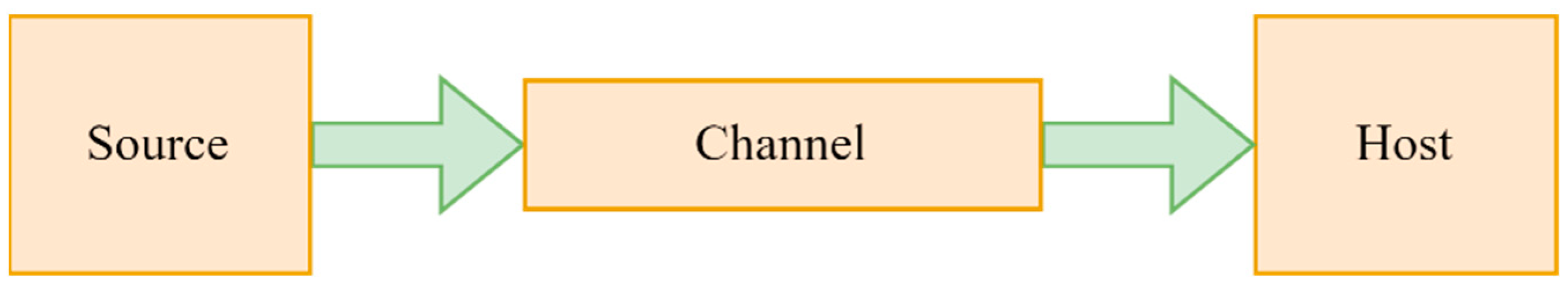
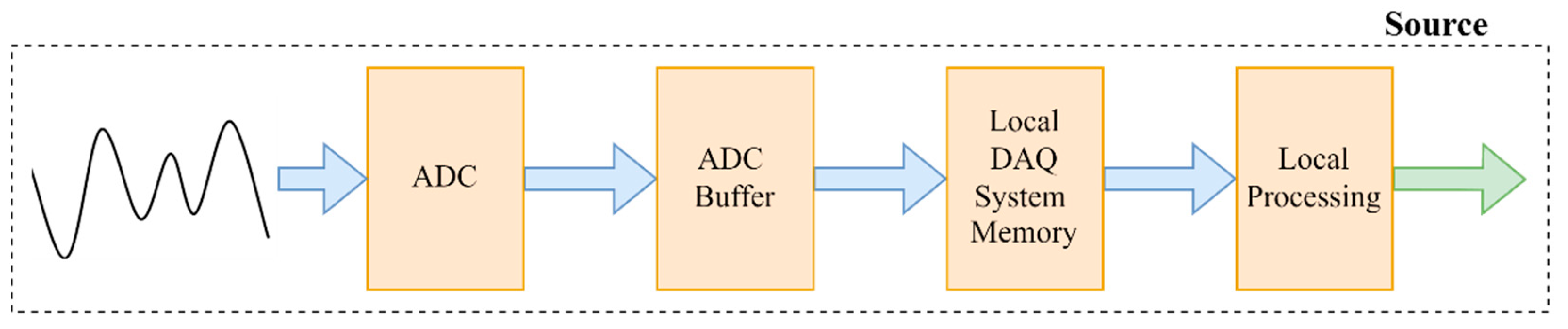

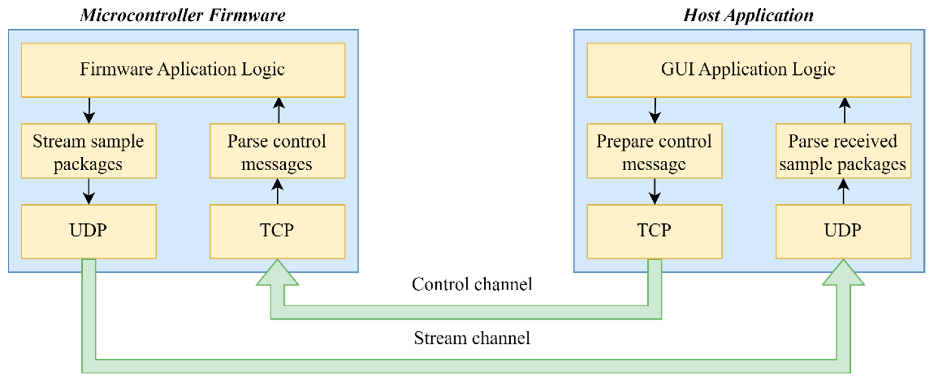

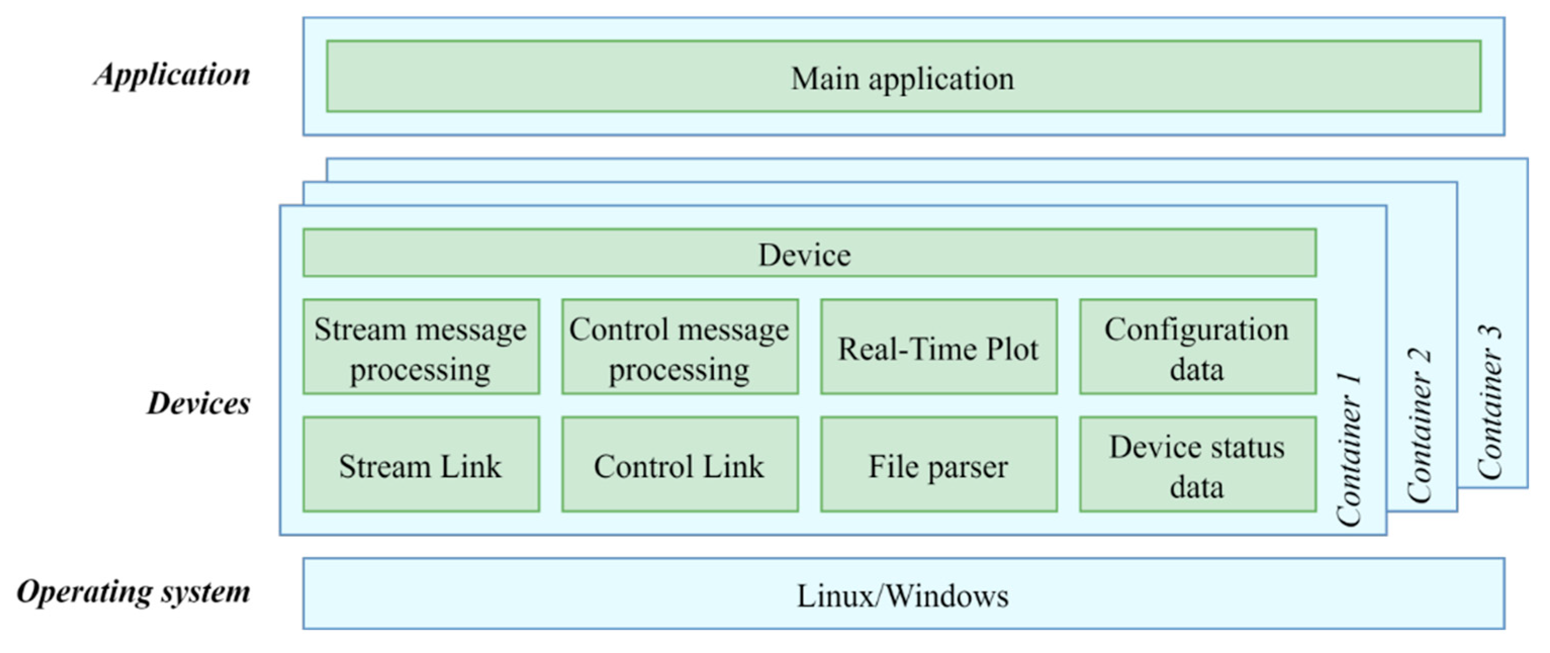
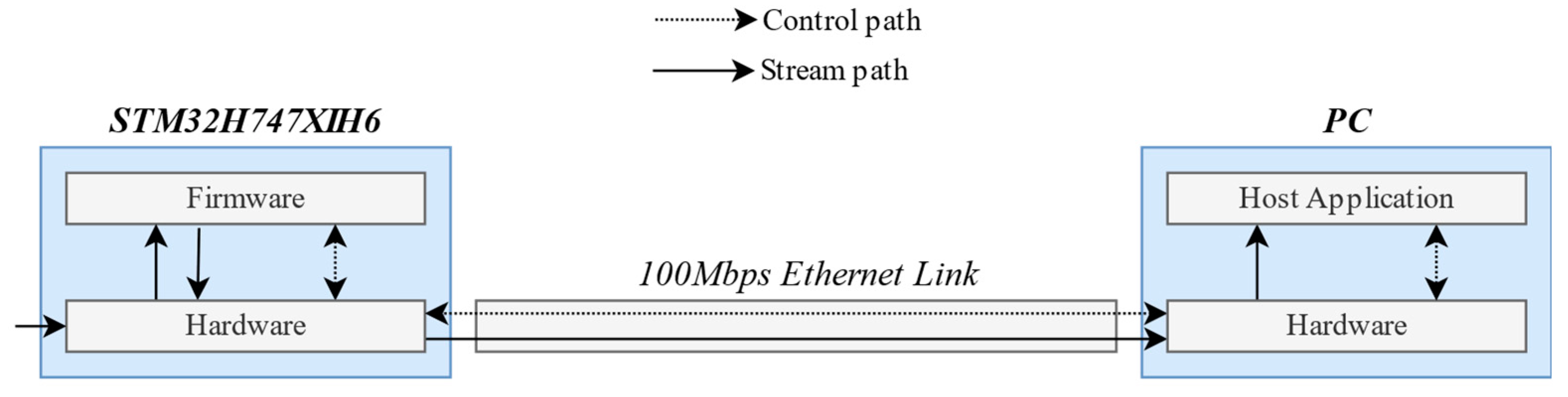

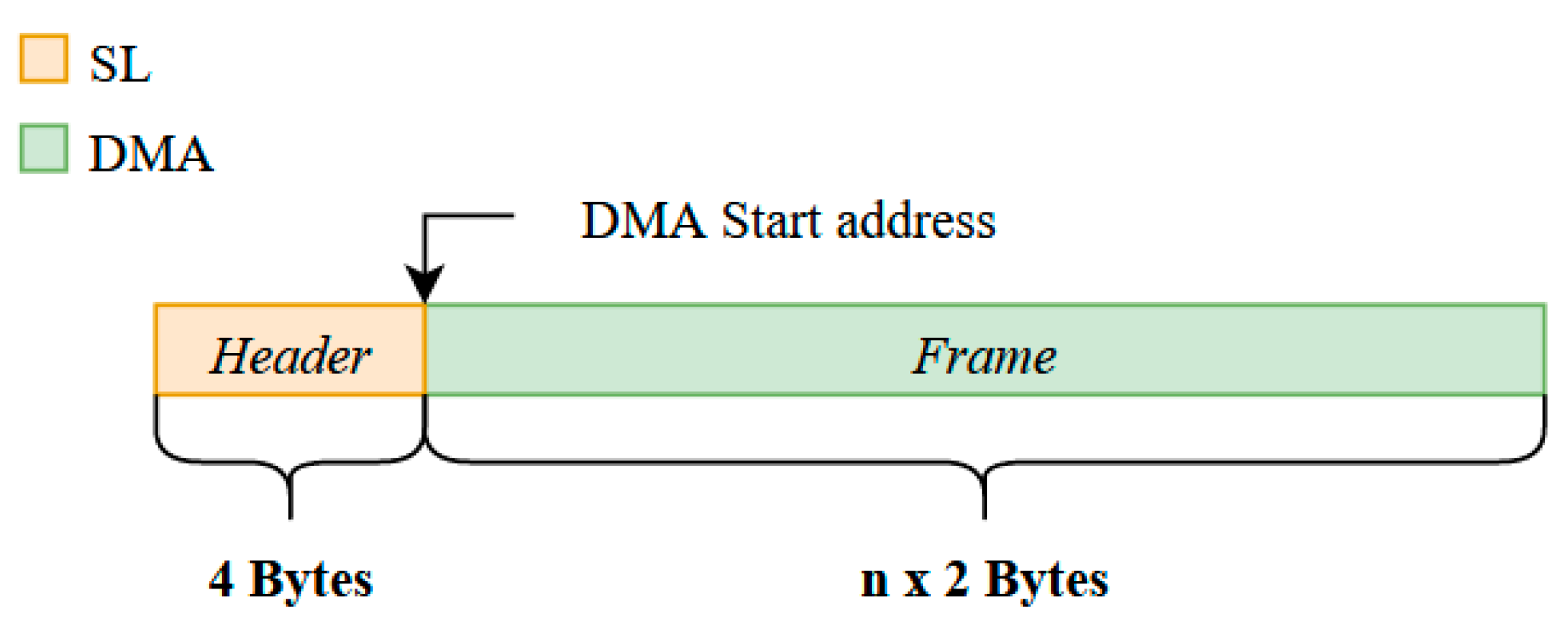

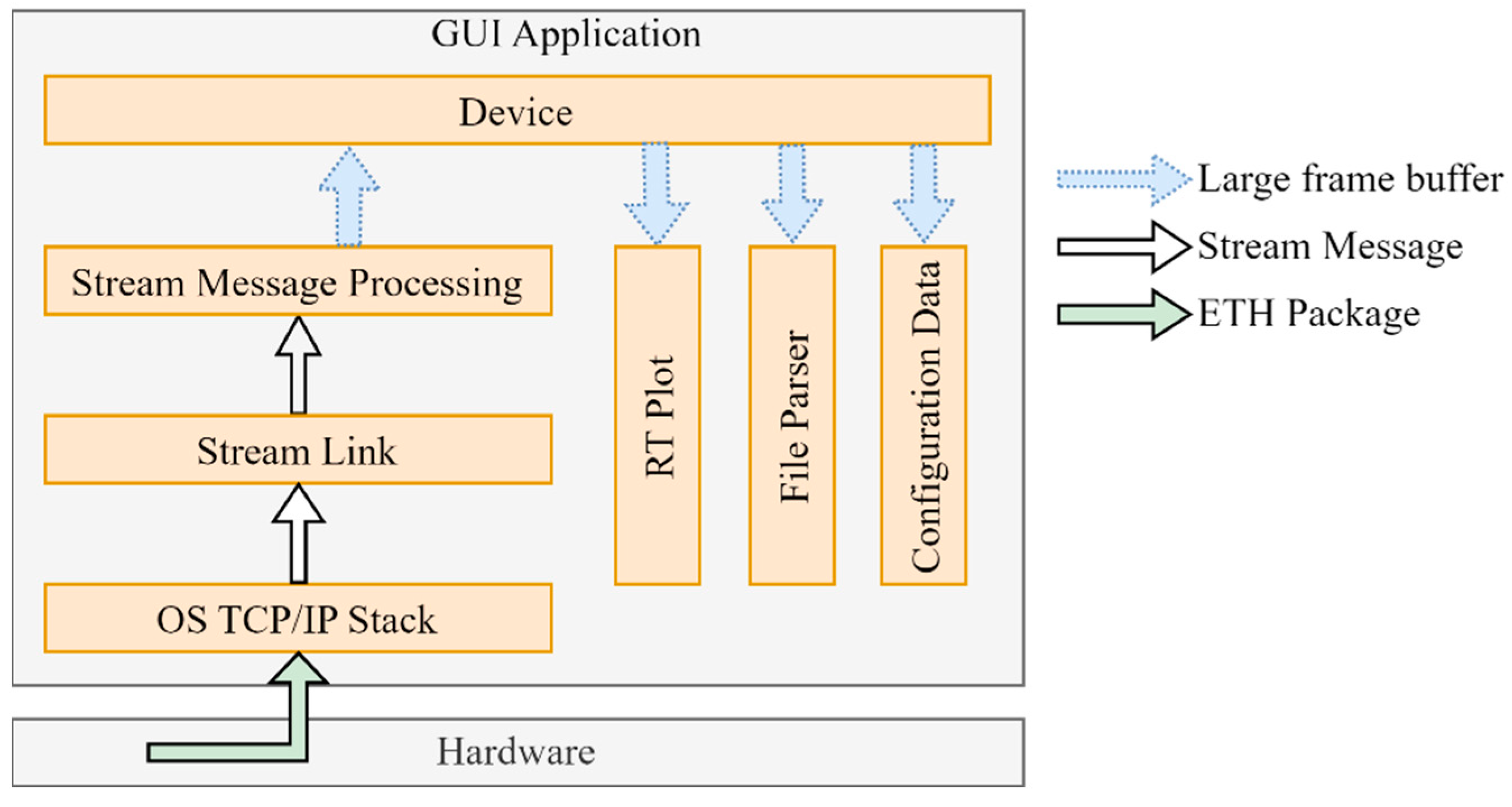
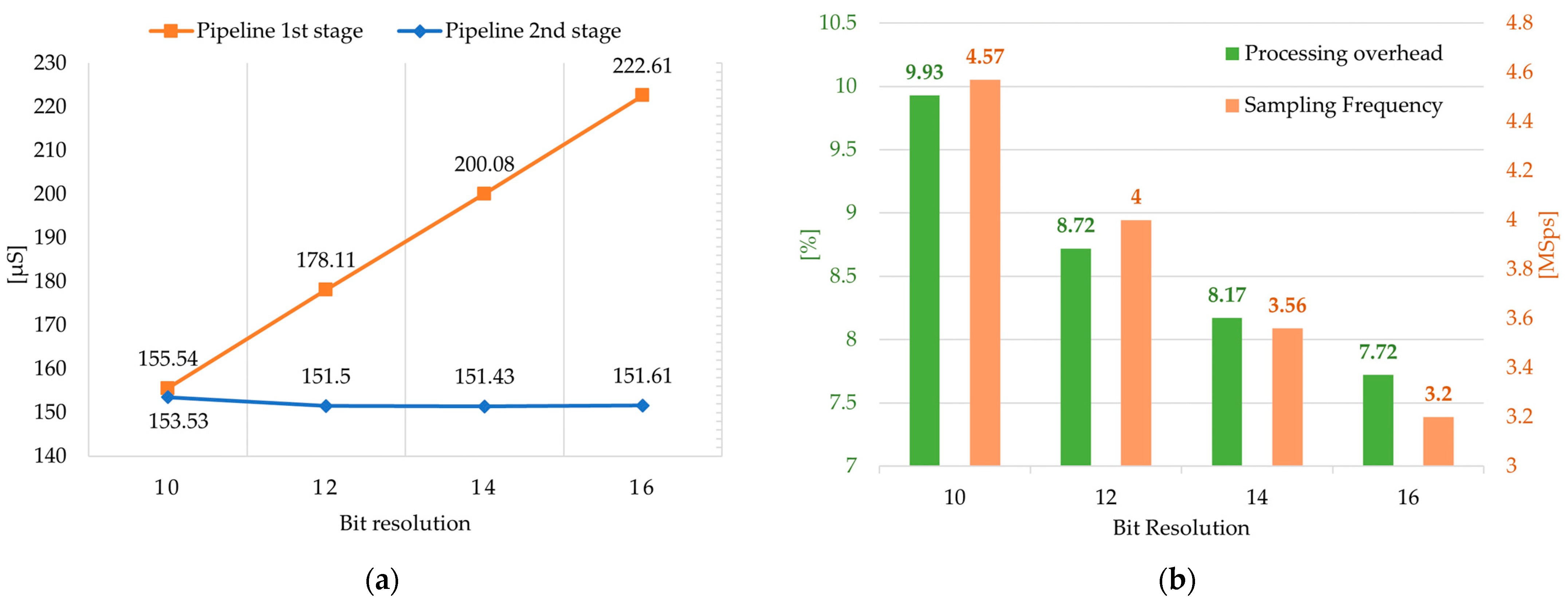

