1. Introduction
In recent years, there has been growing attention in exploiting Internet of Things (IoT) paradigms. This increasing interest followed recent advancements in consumer electronics, communication technologies, cloud computing, and big-data analytics [
1]. In particular, advances in communication performance expected with future millimeter waves 5G and 6G would fully exploit IoT potentialities. This translates into a growing trend of the IoT to absorb many of the different concepts developed in the past. As a consequence, many of the paradigms developed in different contexts, such as smart cities [
2], industrial automation [
3], and home automation [
4] were incorporated within the IoT world thank to its inclusive nature. Particularly, in both of the latter environments above, a very important role in joining the IoT vision is played by the integration of IP-referenced macrosensors based on wireless sensor networks (WSNs) [
5] and including indoor localization [
6]. Nevertheless, many other different environments have been included within the IoT, such as so called intelligent transport system (ITS) solutions and cellular vehicular-to-X (C-V2X) (where ’X’ means vehicles, infrastructures, pedestrians, and networks.). Both ITS and C-V2X are somewhat competitive frameworks of technological developments and applicative models for safety use cases, the management of massive vehicular transports, and the evolution of future autonomous vehicles. Their roll-out in the short term uses radio technologies in the the 5.9 GHz frequency band and for the future fifth-generation of cellular communications frequency bands [
7].Nevertheless, transport management systems widely use radio technologies allocated in the 5.8 GHz frequency band [
8]. These are based on passive transponder technologies [
9,
10] and are spread across many countries in large volumes. Although there exists a regulation about out-of-band spectral emissions, the coexistence of ITS and C-V2X applications, on the one hand, and pre-existing dedicated short range communications (DSRCs) in the 5.8 GHz frequency band on the other, is of concern for the effective deployment of new vehicular communication paradigms [
11,
12]. For this purpose, the European Telecommunications Standards Institute (ETSI) issued a technical specification [
13] where it discussed that, because of the small frequency separation in the frequency band from 5795 to 5815 MHz in use for the EU-DSRC, and the frequency band from 5855 to 5925 MHz in use for the ITS, and considering that both systems operate in road traffic environments, there is significant potential for interference effects between the two communication technologies.
In this paper, we address the impact of a high-Q tuneable band-stop filter to mitigate the specific issue of the mutual interference of ITS and C-V2X to DSRC, providing the design principles, modeling, and experimental data of a dielectric-resonator band-stop filter prototype rendered tuneable by a varactor diode. The paper is organized as follows. In
Section 2, we analyze the specific quantitative issues associated with the mutual interferences between the two communication systems. A description of the filter technology is provided in
Section 3, while its specific design principles are provided in
Section 4. In the same section, we provide the dimensions of the prototype whose characterization is provided in
Section 5. The prototype-equivalent circuit modeling is discussed in
Section 6, which was then adopted to justify the filter features. Lastly, we discuss the state-of-the-art technology of tuneable band-stop filters.
3. DR Tuneable Band-Stop Filter Architecture
In the literature, some techniques for the voltage control of a
-based band-stop filter have been proposed, suggesting, however, complex topologies and designs, such as in [
14,
15,
16,
17]. In particular, the tuneability of
by means of a varactor was demonstrated in different technologies [
18,
19], although their involvement in
band-stop filters was reported in a lower microwave frequency band and while implementing nonplanar control technologies [
17]. In [
20], the authors effectively adopted a microstrip resonator tuned by a varactor pair to adjust the resonance frequency of a band-stop filter; nevertheless, their implementation involved two or more DRs to obtain tuneability and selectivity.
In this context, this paper presents an effective technique to control electronically DR-based band-stop filters that are suitable to enable the coexistence of ITS and C-V2X applications with 5.8 GHz DSRC-based applications and vice versa. The proposed approach is based on the combination of two different stop-band filter technologies: one implementing a DR resonator coupled to a transmission line, and the other based on a varactor tuned microstrip ring resonator, thus avoiding any tuning mechanical needs and making the control fully planar.
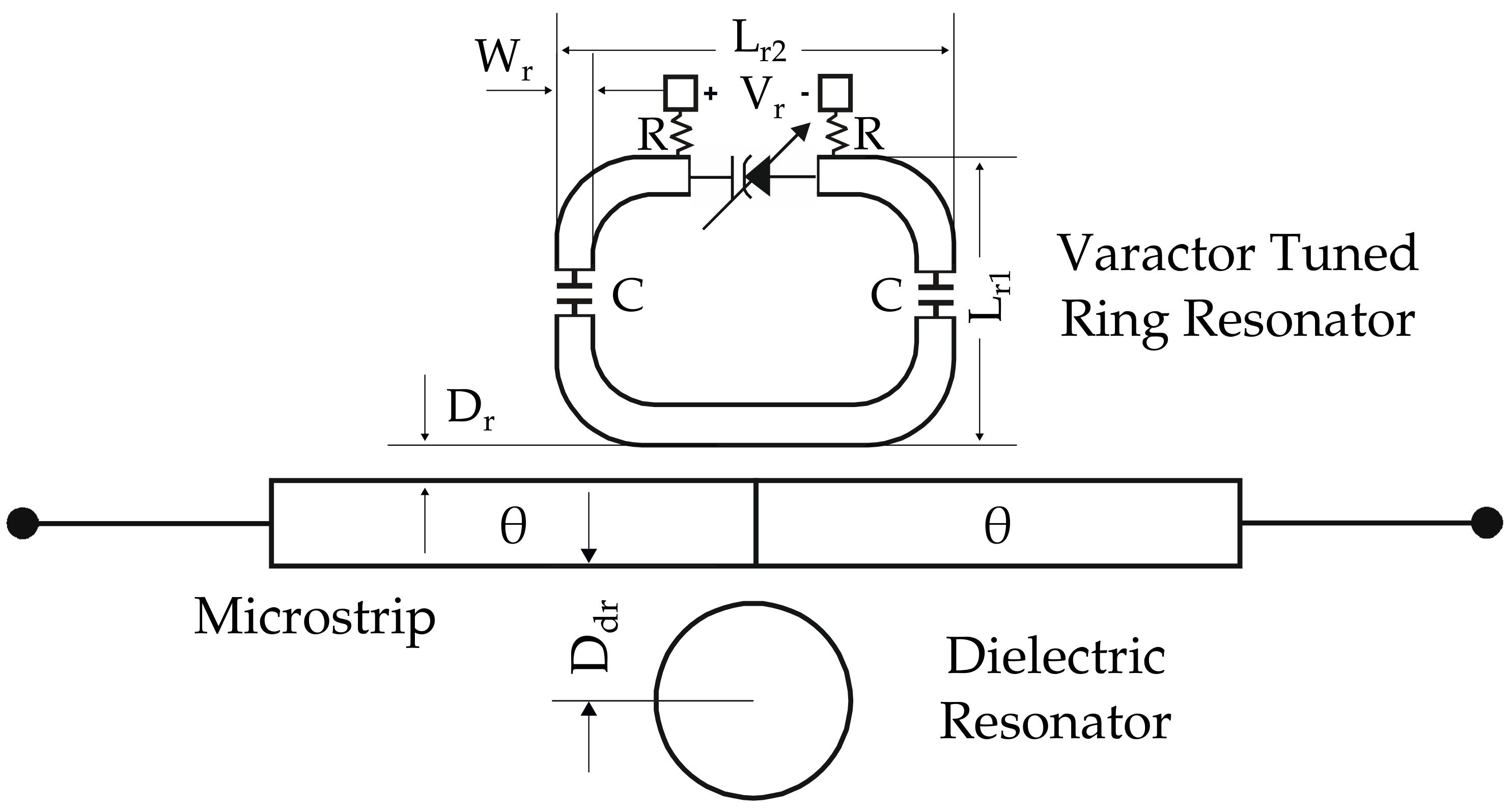
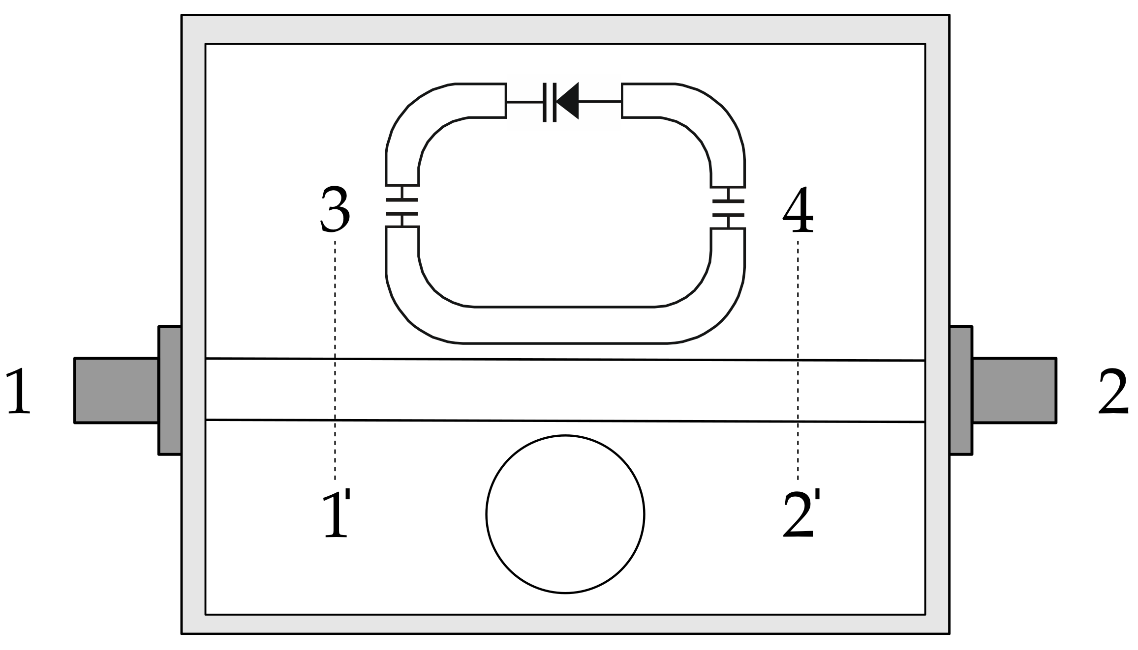
As depicted in
Figure 1, the structure of the proposed band-stop filter involves a disk-shaped DR and a planar microstrip ring resonator coupled to each other via a microstrip transmission line; this concurrent coupling between the two resonators enables the merging of their resonance behaviors. The figure reports the main geometric dimensions of the filter structure.
The electronic control of the band-stop filter resonance was obtained by varying the equivalent capacitance exhibited by a varactor diode inserted into the microstrip ring. The proposed arrangement provides some advantages, such as achieving a tighter coupling between the ring and the microstrip line, and the full planarity of the DR filter controlling parts. The varactor bias circuit is shown in
Figure 1, where a pair of high-value resistors, R, act as choke, while a couple of capacitors prevent device shortcircuits and preserve ring symmetry. The conventional DR operation mode assumes a filter enclosure in a metallic box, which determines establishing the cavity modes and filter performance. For this reason, the filter was enclosed in an aluminum metal box whose internal dimensions were
mm
.
4. Design Principles
As a basic design principle, we assumed that the two resonators, considered separately, exhibited the same resonance frequency. In addition, a rather realistic assumption was that the two resonators were not directly coupled, as in previous works, but interacted through the microstrip line connecting the two filter ports. The ring resonator design criteria are those related to the ideal structural design relations outlined in [
21].
The band-stop filter design was optimized with respect to the specific requirements for vehicular DSRC applications at 5.8 GHz, which are four carriers colocated in the 5795–5812.5 MHz spectral range, and a pair of carriers at 5.8 and 5.810 GHz on a regional basis. This leads to a design approach aimed to maximize the filter Q factor with respect to the tuning range. The filter was implemented on an organic–ceramic substrate with a thickness of 1.27 mm and an , and adopted a SMV2020 hyperabrupt varactor diode as the tuning element.
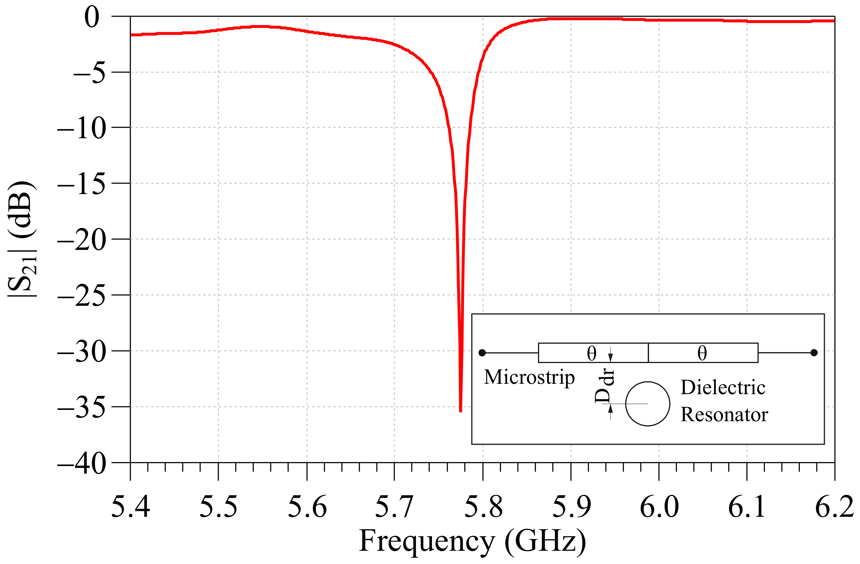
The first step of the design procedure was the design of the DR band-stop filter, which began with the identification of a DR exhibiting a resonance at the central frequency of 5.8 GHz. For this purpose, a DR was selected with the following characteristics (Exxelia E4000 series): height 5 mm, diameter 11 mm, relative dielectric constant
, and unloaded Q factor of about 15,000 at 10 GHz. The performance of the resulting DR-based filter within the cavity, optimized in accordance with the procedure described in [
17], is reported in
Figure 2. The insertion loss at 5.8 GHz was 36.5 dB, while at 5.9 GHz, it was 0.6 dB; the optimal value of about
mm was found.
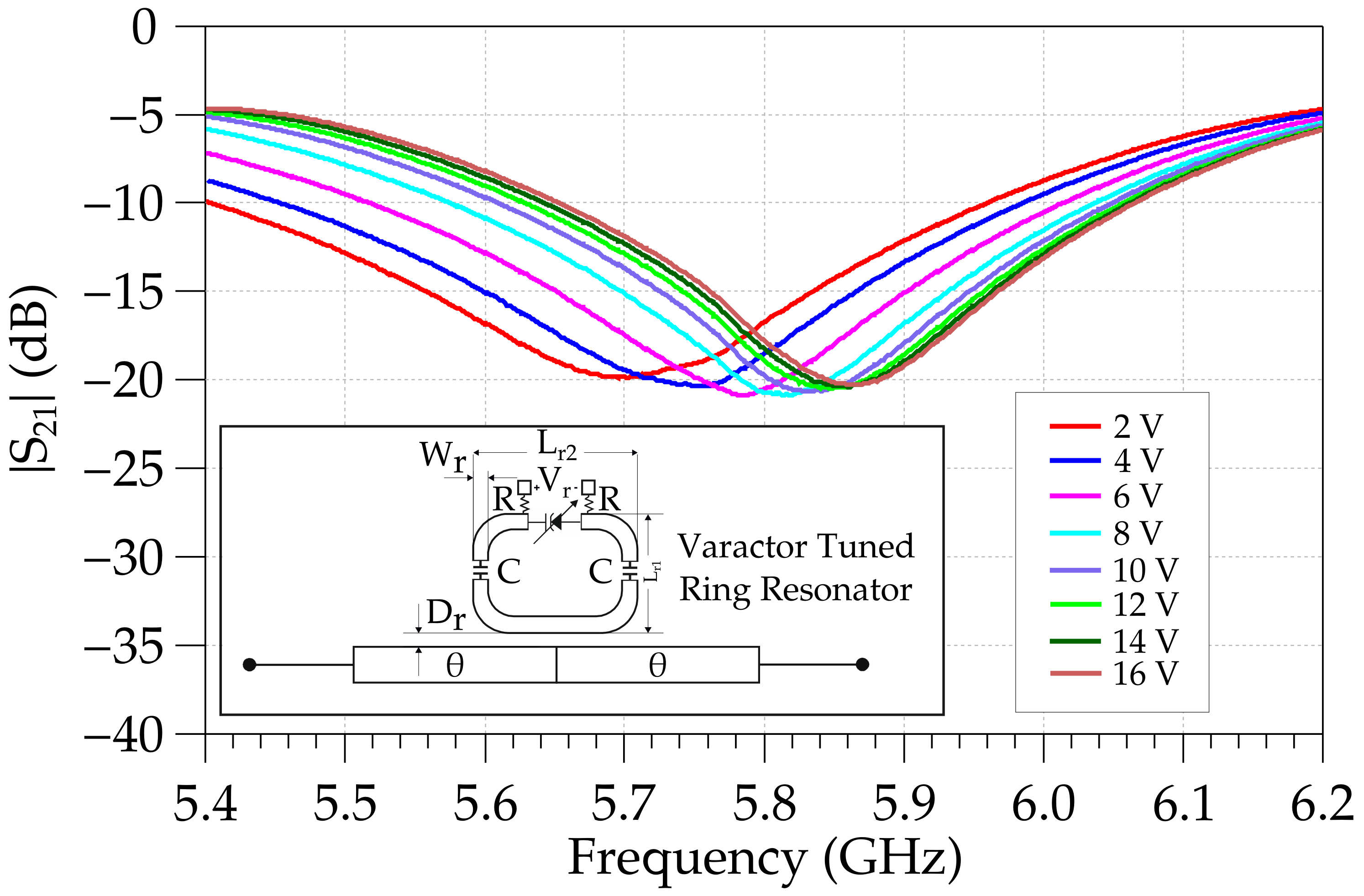
The second step consisted of designing the tuneable ring resonator at the reference frequency. This was based on a microstrip ring with length equal to the wavelength at the central frequency, interrupted by the varactor and decoupling capacitor pair.
Figure 3 reports the measured performance of the latter at different varactor bias voltage levels. The filter showed relatively poorer Q-factor performance, while it was optimized to maximize its tuning range, which was from 5.68 to 5.86 GHz. The resulting optimal values were:
mm,
mm,
mm, and
mm.
The third and final step began with merging the two structures by means of a unique microstrip, as described above. The performance was optimized by running full 3D electromagnetic simulations involving the whole tuneable filter and the metal box. This optimization procedure led to a slight change in the and parameters. A target value larger than 90 for the Q translated into the optimal values of mm and mm.
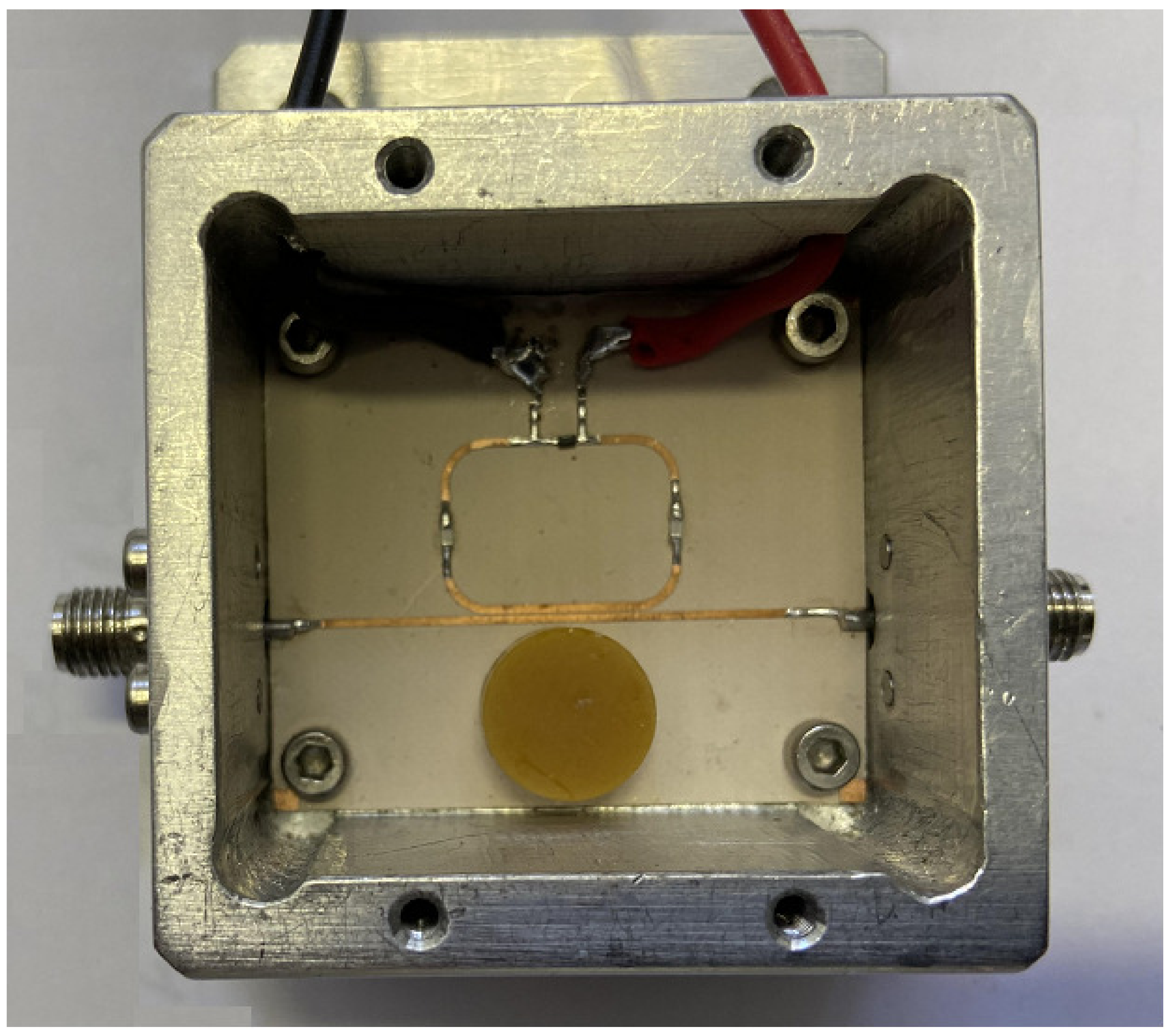
5. Filter Prototype Characterization
A picture of the varactor-tuned DR band-stop filter prototype resulting from the proposed design procedure is shown in
Figure 4, and
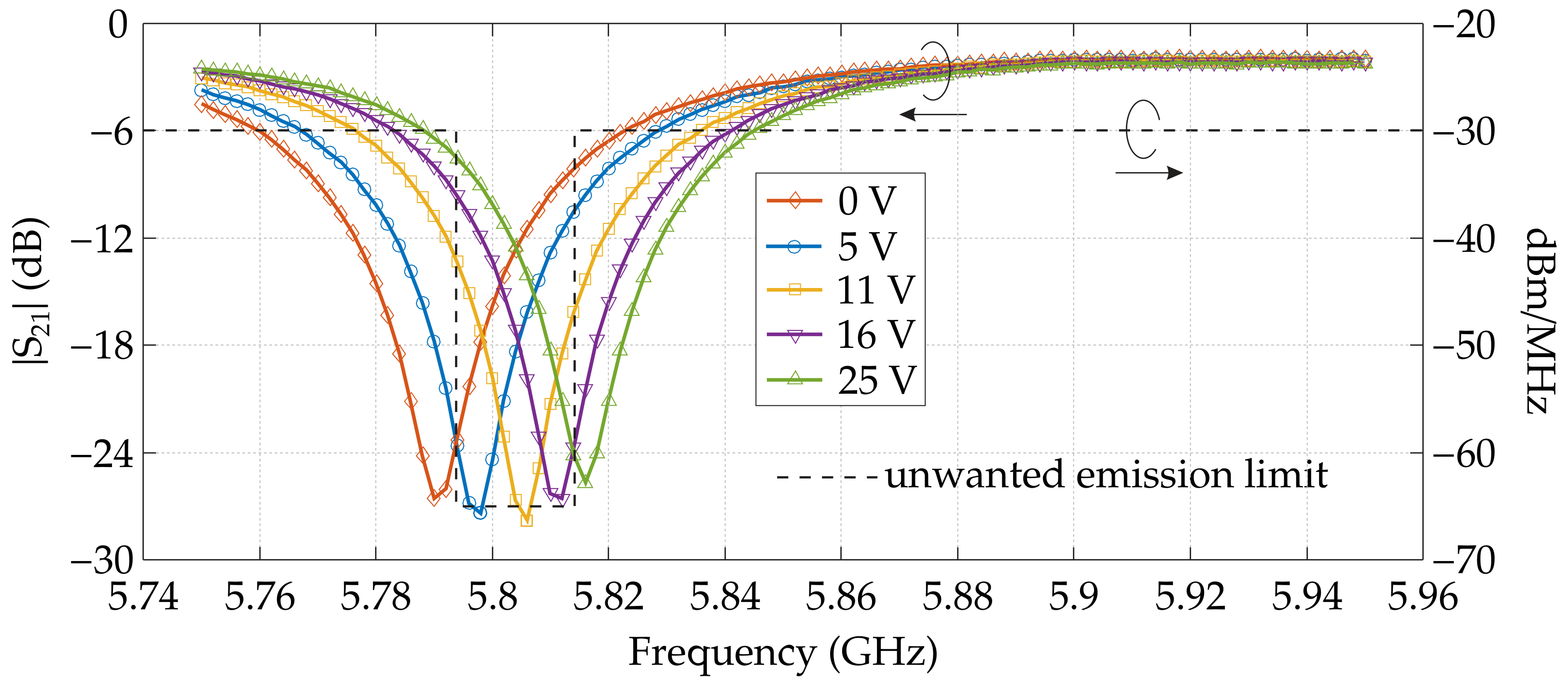
Figure 5 reports its characterization achieved by a calibrated vector network analyzer across the bandwidth of 5.75–5.95 GHz, with control bias
spanning from 0 to 25 V. The same graph reports the unwanted transmitter emission limits for the ITS frequency band [
13]. Transmission parameter
exhibited a tuned frequency response band-stop depth in excess of −25 dB within the frequency tuning range spanning from 5.794 to 5.814 GHz (20 MHz). The measured maximal insertion loss at 5.9 GHz was 1.6 dB.
Table 2 summarizes the estimations from the experimental data, resonant frequency. and the loaded Q factor across the tuning range. The Q factor was calculated with the ratio of the resonance frequency and
(bandwidth at half minimal insertion loss), and its estimation provided values in excess of 90 across the entire tuning range, while the resonant frequency covered the entire set of frequency channels of the European DSRC vehicular applications at 5.8 GHz [
8].
Regarding the validation of the proposed electronic tuneable DR-based band-stop filter,
Table 3 presents a comparison between the characteristics of the prototype and those associated to a benchmark, which is a conventional version of the band-stop filter based on the same DR, dielectric substrate, and metal box, and tuned by means of a tuning screw metal plate as described in [
22]. Compared to the benchmark, the results show that the proposed prototype exhibited slightly worse performance at the same resonance frequency. In particular, it provided comparable tuning range and stop-band rejection, although with a reduced Q factor. The advantage introduced by this planar and cost-effective electronic tuning implementation compensates for the moderate degradation of the frequency selectivity while maintaining comparable tuning capability with respect to the mechanical tuning.
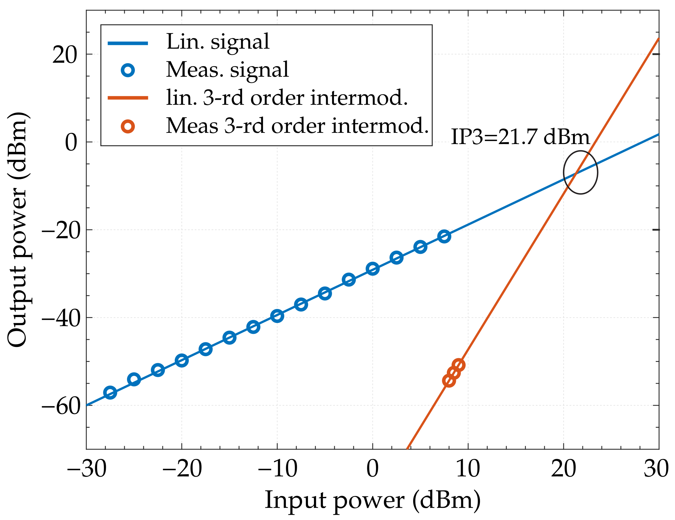
As discussed above, the coexistence of emitted EU-DSRC interference vs. ITS also requires high linearity in the filter response. In order to fully characterize the DR filter in terms of linearity, the IP3 response was evaluated. The characterization was carried out by means of a vector signal generator capable of providing two EU-DSRC carriers at the filter prototype input terminal, and a spectral analyzer to evaluate the third-order intermodulation products.
Measurements were carried out regarding the power of the two carriers at 5.805 MHz and 5.795 GHz tones, from −30 to 12.5 dBm, biasing the filter at
= 10, which corresponded to a resonance frequency
of about 5.8 GHz.
Figure 6 reports the results, showing an input IP3 response of about 21.7 dBm.
6. Filter Modelling
A previous study [
22,
23] demonstrated that both DR and ring resonator filters can be modeled according to a series of RLC circuits regarding resonance frequency. In [
24], the authors derived the equivalent circuit parameters via numerical electromagnetic simulations. In this paper, we derived an equivalent circuit model for the varactor-based tuneable DR band-stop filter of
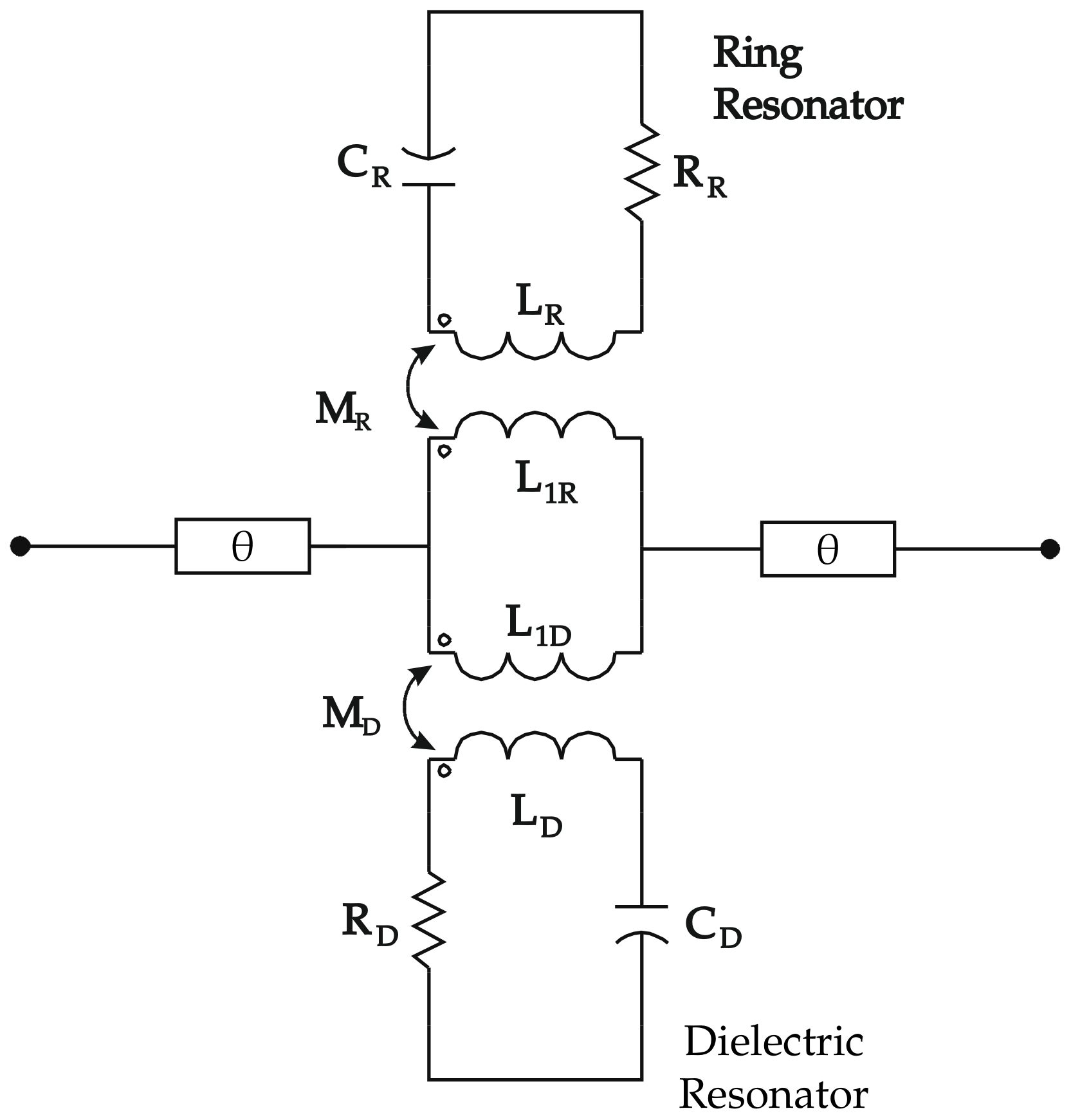
Figure 1 that is capable of providing insight into its mode of operation, justifying the design principle discussed above.
The first step of the analysis was to model both the DR and the ring resonator via the corresponding resonant RLC series circuits. Then, in accordance with the assumption that the main coupling effects occurred between the transmission line and the ring, on the one hand, and between the same transmission line and the DR, on the other hand, we could infer the equivalent circuit model depicted in
Figure 7. In this model, the coupling between the two resonators and the microstrip line was modeled with a pair of mutually coupled inductors [
25] whose equivalent circuit lumped elements,
,
and
,
, should be identified via either accurate full-wave simulations or an experimental characterization.
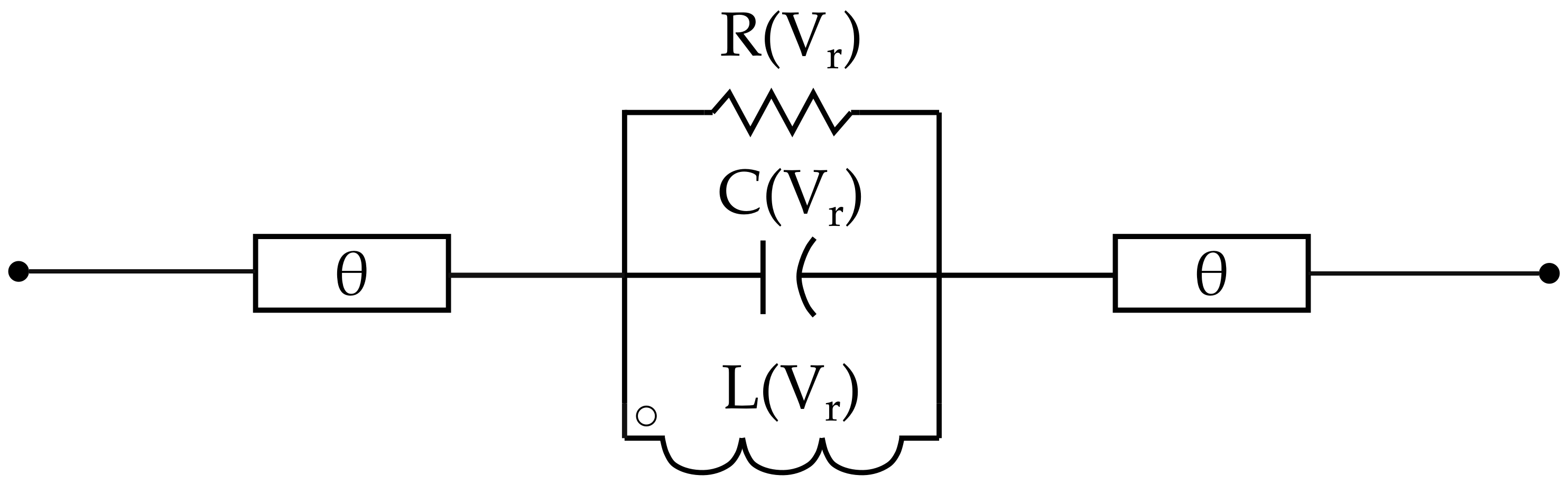
By means of circuit analysis techniques, the circuit model could be conveniently reduced to the single resonant RLC parallel circuit shown in
Figure 8, which represents the interaction of the two resonators and their coupling to the microstrip line. The identification of the reduced equivalent circuit parameters was as follows.
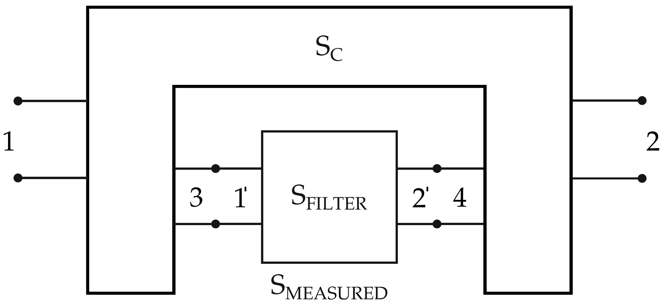
In accordance with the general technique of DR-based band-stop filters, these operate embedded in a cavity implemented by a metal box, along with the interconnecting transmission lines (of electrical length
, cf.
Figure 1). Thus, the first step of the equivalent circuit model extraction requires a de-embedding procedure in order to completely remove the interaction between the metal box and the DR, and the feeding microstrip connecting the filter with the connectors; all these parts were included in the 4 × 4 scattering matrix
; cf.
Figure 9. We extracted the
matrix with a full-wave 3D electromagnetic simulation further validated by calibration procedures; cf.
Figure 10.
The next step consisted of extracting the
matrix, as described in [
26], and applying it to the structures illustrated in
Figure 10. The
matrix was then associated with the reduced circuit model in
Figure 8. Using the measured data and the constituent relations, defined with regard to the resonance frequency
, we calculated the equivalent circuit parameters as follows:
where
are the Z parameters derived from
,
is the full width at half maximal insertion loss bandwidth, and
is the system impedance.
For the prototype shown in
Figure 4, the de-embedding procedure led to the characterization of the intrinsic band-stop filter identified by port numbers
and
in
Figure 10; a comparison between measurements and extracted intrinsic filter behavior is shown in
Figure 11. From the comparison, we can recognize a slight deviation of the resonant frequency due to the secondary effects of the metal box and the interconnecting transmission lines.
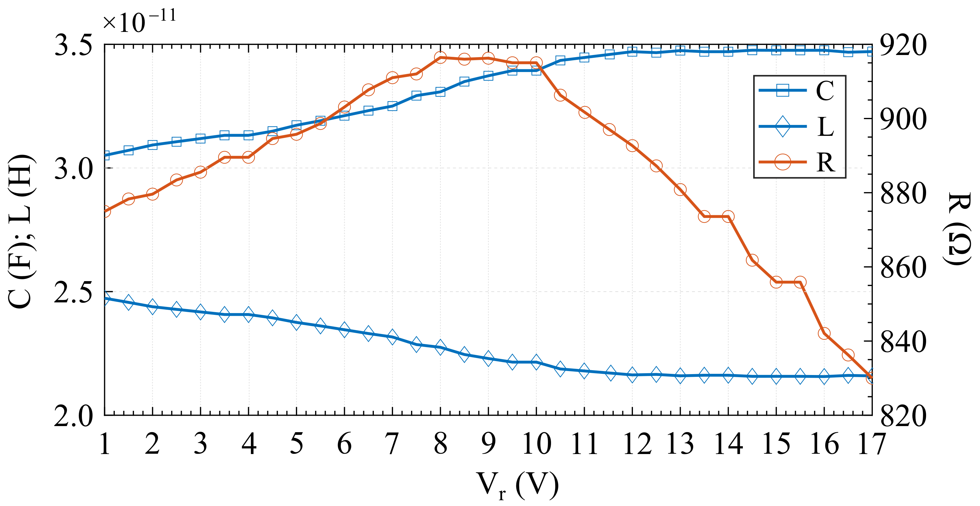
The above-described procedure applied to the de-embedded data led to parameters
of the derived equivalent circuit model of
Figure 8, as functions of control voltage
that are reported in
Figure 12. The figure shows slightly opposed trendsfor the equivalent capacitance and inductance behavior versus the bias voltage, and an equivalent resistance maximum at the bias voltage corresponding to the peak of
.
Figure 11 shows a comparison between the frequency response of the equivalent parallel RLC circuit, calculated at
V, and the corresponding experimental data. We can see the accuracy of the model in predicting the de-embedded filter response, especially in the vicinity of the resonance frequency, thus validating the proposed modeling and analysis.
As stated previously, equivalent resistance
modeled the insertion loss of the tuneable DR filter at the resonant frequency
corresponding to the bias voltage
, where the filter impedance was purely resistive. Extrapolated values
are reported in
Figure 8.
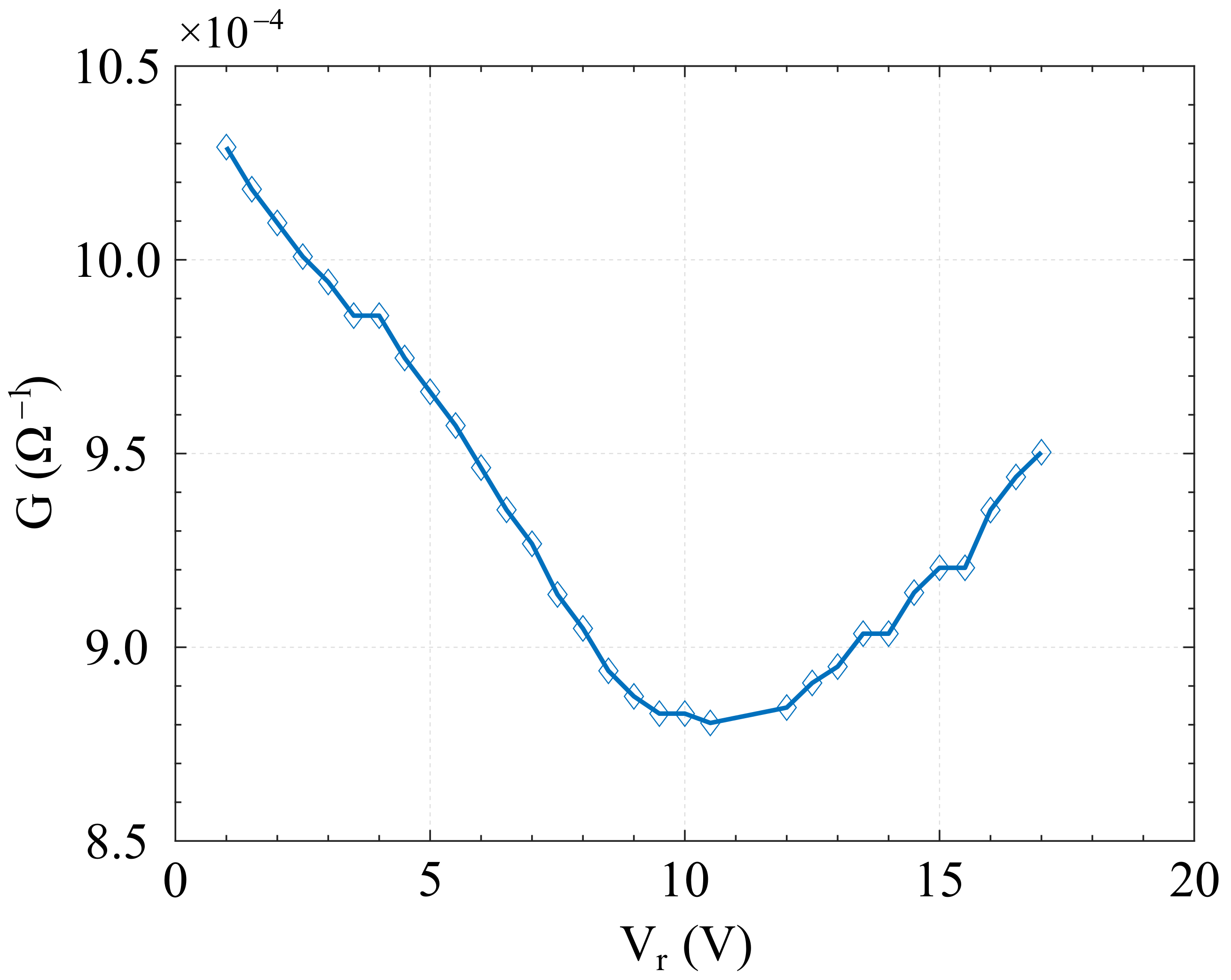
At resonance,
was responsible of the filter nonlinear behavior. By inverting
, it is possible to evaluate the corresponding behavior for conductance
.
Figure 13 reports the calculated nonlinear conductance.
Knowledge of nonlinear conductance
=
allows for the evaluation of the input third-order intercept point (
) to be performed with a simple and intuitive approach [
27,
28]. In particular,
=
must be expressed by a polynomial as in Equation (
5)
In this circumstance, it is possible to directly calculate IIP3 using the following expression:
In our modeling procedure, the polynomial expression of nonlinear conductance
=
(
V) for a certain
=
was simply obtained from the
G =
by first shifting the origin of the curve in
, and then calculating the polynomial coefficient as the one at the minimal distance from the extrapolated value with a proper order. In the interpolation procedure,
was set at 10 V, and the corresponding shifted curve is illustrated in
Figure 14, which also shows the polynomial at the minimal distance from the extrapolated value. The best fitting was obtained with a sixth-order polynomial whose corresponding expression is reported in Equation (
7).
The calculated polynomial showed, for the first-order and third-order coefficients the values of = and = , respectively. This led to a calculated linear of about 13.08 that translated into a dB lead to a = 22.3 dBm, while the measured one was 21.7 dBm.
7. Technological Comparison
The aim of this section is to compare the available technology to implement a microwave tuneable band stop filter. The target was to identify the better technology to implement the optimal filter, and improve ITS and C-V2X coexistence with vehicular DSRC.
The core of this analysis is represented in
Table 4. This table is the result of the accurate analysis of the literature related to tuneable band-stop filters for microwave applications. The focus mainly consisted of varactor-diode-tuned filters, but microelectromechanical system (MEMS)-based technologies were also taken into account.
Table 4 summarizes the performance of different band stop filters implemented in different technologies, and compares their performances in the context of ITS and C-V2X coexistence with vehicular DSRC. Data were extrapolated from previous studies reporting filter prototypes also operating in different frequency bands from the object of the present work. Each of the referenced works was considered to be representative of a given technology and topology. As a result, the considered technologies in this analysis were the use of a single-stage DR and varactor diodes, double-stage DR and varactor diodes,
strip resonator and varactor diodes, frequency selective surface (FSS) and varactor diodes, substrate integrated waveguide (SIW) and varactor diodes, and 2-bit microelectromechanical systems (MEMSs). The comparison reported in
Table 4 is based on the extrapolation figures of merit that were independent from resonance frequency
, such as the Q factor,
band, max rejection loss (
) within the pass band, insertion loss (
) in the pass band located at 1.8% of
, and tuning range. The first and last columns refer to the operating resonance frequency
and the filter technology, respectively. This approach allowed for fully comparing the filter performance independently from the specific frequency of operation.
From an application point of view, an optimal filter for the coexistence between the two communication systems should feature a high RL with a low
band with respect to the EU-DSRC spectrum when implemented at the output of the ITS transmitter, and the lowest IL in the spectrum of the ITS when implemented at the input of the ITS receiver.
has to be better than −25 dB, while
has to be less than 2 dB. On this basis, the critical analysis on the available data reported in
Table 4 highlights that only two of DR-based tuneable filters exhibited compatible performance with such coexistence requirements. In particular, the better trade-off in terms of performance and complexity was by the filter described in the present paper. The filter in [
20] had comparable performance with the one proposed in this work, but with an increased level of complexity because it adopts a two-stage topology.
8. Conclusions
This paper described the structure and design principles of a tuneable DR band-stop filter that is suitable for the coexistence of ITS and C-V2X with vehicular DSRC at 5.8 GHz. The filter was based on a disk-shaped DR coupled via a microstrip transmission line to a planar microstrip ring resonator, and it was tuned by varying the bias voltage of a varactor diode inserted into the ring. The design principles were validated with the realization of a prototype that exhibited a loaded Q exceeding 90 across the tuning range from 26 MHz to about 5.8 GHz, with a rejection better than 25 dB. Its performance and that of a benchmark developed at the same operating frequency were compared, but implementing mechanical tuning on the basis of the same DR showed comparable resonant frequency tuneability.
We illustrated and validated an equivalent circuit via the characterization of the tuneable DR band-stop filter prototype. The former was adopted to discuss the filter response in the linear and nonlinear regimes, and its capability to predict filter performance in terms of intermodulation product generation. For the first time, this paper discussed the linearity issue of tuneable band-stop filters in the context of the coexistence of communication systems.
A comparison with the state of the art demonstrated that the discussed prototype enabled the coexistence of vehicular DSRC and ITS/C-V2X communication systems operating in the 5.8/5.9 GHz frequency band because of its trade-off between the stop-band RL and the pass-band IL with a minimal number of tuneable elements and DRs.


