Featured Application
Presented controller synthesis strategy applies to systems running under tight time dependencies and requiring precise and repeatable timing of operations. The presented solution is used in PMSM drive control but also can find an application in inverters drive.
Abstract
Implementation of the permanent magnet synchronous motor vector control implies strong time dependencies. The control process requires precise measurement of motor shaft position and winding currents to establish correct driving. The tight time dependencies are difficult to achieve using a programmatic approach. Specific controller architecture is proposed for programmable systems on chip architectures enabling operations precise timing and improved processing performance. The controller is decomposed into a dedicated hardware interface system and programmatic part for easy implementation and modification of the control algorithm. The proposed architecture offers precise and repeatable input-output operations timing and assures meeting tight time dependencies. The control algorithm is executed as an interrupt service requested by the interface system in a constant processing period with relatively weak time dependencies. Additionally, the interface system preprocesses input and output signals reducing the computation effort and saving time for algorithm computations. The specific implementation enabled improved measurement of the motor’s windings current with suppression of disturbances caused by inverter operation. There is shown an efficient implementation of Parke’s and Clarke’s transformations using specific resources of modern programmable logic devices. In opposite to the software-managed implementation presented implementation assures completing processing faster, using a minimal number of hardware resources of the FPGA platform and offering the highest flexibility of software part implementation.
1. Introduction
Permanent magnet synchronous motors (PMSM) are the most promising solutions for power drive systems including transportation systems. High efficiency and large torque along with small size, weight, and simple construction are its short characteristics [1]. The motor stator is similar to the stator of induction motors while the rotor consists of permanent magnets. The magnets and the armature winding are positioned so that the electromotive force generated as a result of rotation is sinusoidal. PMSM motors can operate at a wide range of rotation speeds offering flexible driving capabilities [1,2].
These motors require a power electronic drive system, typically using field-oriented control to be efficiently driven [3]. The motor controller operates in tight time dependencies. The available time for the controller is determined by the base period of the power inverter. It is essential to work out the driving parameters of the inverter for each period based on evaluated signals. This makes the most critical task of controller implementation [4].
The other essential problem is the operation safety of the insulated gate bipolar transistor (IGBT) power components. It is important to correctly drive complementary pairs and immediately react to overloading conditions. The tight time dependencies and requirements of synchronous operation of input signals acquisition and respective outputs controlling make the software implementation using a typical microcontroller very difficult or almost impossible [5]. The dedicated direct hardware implementation is the opposite choice [6,7,8,9]. Due to implementation complexity, specific skills are required. It is not suitable for wide use by automation engineers. The solution should combine the easiness of programming with the exact timing of input-output operations. There exists an implementation trap caused by improperly used high-level synthesis tools [10]. A superficial analysis of requirements results in significant implementation overhead both resources and computation time as well unnecessary programming complexity.
The paper proposes the nonstandard implementation of a controller utilizing the ZYNQ Programmable System on Chip (PSoC) architecture [11]. It allows for the development of a system that utilizes the complex hardware peripheral system implemented in a Field Programmable Gate Array (FPGA) structure and linked with a programmable system driven by a dual-core ARM Cortex A9 processing unit.
1.1. The PMSM Controller Architecture and Requirements
The field-oriented control system block diagram is shown in Figure 1. The controller structure has been partitioned into blocks depending on its functionality that constitute 4 layers. The controlled object consists of the motor with an IGBT-driven inverter and respective sensors determining its operation conditions. The motor shaft position and winding currents sensing are essential for working out driving signals for the inverter.
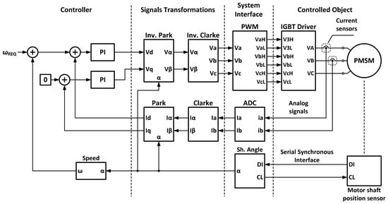
Figure 1.
The general structure of the PMSM control system.
The next layer named a system interface is responsible for exchanging signals between the controlled object and the core controller. The IGBT power stage [12] is driven by a pulse width modulation (PWM) unit with 3 complementary operating channels. The PWM driving principle is based on push-pull driving with an appropriate proportion between both activities that correspond to the requested output voltage (an average voltage of a switching power supply). To avoid the simultaneous activity of both transistors (resulting in instant damage of a bridge) of the quasi-complementary IGBT stage there must be inserted a dead time gap allowing for the undriven transistor completely switch off. To eliminate power stage damage possibility the dead time gap must be assured by its hardware structure.
The motor operation conditions are observed using winding currents and shaft position. The current sensors are placed on the power lines of the motor. The winding currents measurement process requires the elimination of disturbances generated by the inverter operation [13,14] assuring a recent period average current delivery. Along with the current measurement the shaft position is measured. In the experimental model, the absolute position encoder unit with a serial synchronous interface (SSI) is used [15]. The moment of position measurement is synchronized with the current measurement to keep the relation of currents and the shaft position for further computations.
The next layer called signal transformations consists of input and output paths. The input path is aimed at preprocessing measured values for the control system. The input path transforms the current values ia and ib from a 3-phase system using Clarke (iα, iβ) and Park transformations to the static vector reference system id, iq and angle α [16]. The output path is responsible for translating what has been worked out by the controller Vd and Vq voltage static vector system to appropriate control signals for the PWM controller.
The control system is the last block that closes the control loop. Based on the motor operation conditions [id, iq, α] and required operation parameters (here limited to required rotation speed ωREQ) computes the required driving parameters of the inverter. This part of the controller is implemented in software giving an opportunity to easily accommodate control logic implementation to the needs. The diagram shows an exemplary control unit that minimizes the iq current and accommodates the Vd voltage to the required speed. To simplify the software design the control function is implemented as an interrupt handler. The hardware front-end layer manages the timing dependencies of all operations while the software part is expected to deliver motor driving parameters only.
1.2. High-Performance Controller Concept for Tight Time Dependencies Systems
The essential problem in implementing the control systems operating under tight time conditions is assuring completion of all processing and measurement tasks in a given time according to the schedule of operation that is especially important for input signals measurements (ADC sampling, external measurement device triggering and response processing). This puts the problem of time predictability of a computation system [5]. The commonly used microprocessor systems are derived from microprogrammable control systems. The execution time of digital systems is well described by the number of clock cycles that correspond to the execution time. Microprocessors are digital systems that optimization was pushed toward fast and efficient execution of instructions [17]. Introduced improvements in the instruction execution system like pipelined execution (pipe flushing on jumps), and cache memories (cache mishit problem) the problem of execution time make complex and difficult. Even for a simple microprocessor implementation, the execution time estimation is a difficult task due to multiple conditional paths and internal program state dependencies. This results in imprecise operations timing (variation of the moment in time an operation is executed). To makes things more complex use of different peripheral units that are only software-linked makes it impossible to achieve synchronous operation of all units assuring the exact in-time operation of multiple peripheral units as required for the considered control system. It should also be observed that increasing the speed of the processor and the complexity of the system results in the hierarchical implementation of the internal bus system. In other words, the input-output peripherals are located behind several bus system crossbar layers (e.g., AXI). This extends the data exchange time between the processor and peripherals.
The paper proposes the architecture of a controller for driving permanent magnet motors using ZYNQ device [11]. There is shown the implementation methodology of the integrated hardware-software system which assures precise timing with a resolution of 1 period of the peripheral clock signal. The goal is achieved by implementing an integrated hardware interface that manages measurement and driving operations according to a deterministic schedule. In the proposed architecture time dependencies for software implementation are reduced allowing for completing computations in a relatively wide time window. Moreover, the hardware platform is capable of observing the control processing loss in time cycles. The proposed architecture allows for a simplified control algorithm implementation while all tasks requiring precisely timed operations are managed by a dedicated hardware platform implemented using the FPGA part of the ZYNQ device.
The paper is outlined as follows. The next section analyses the architecture of the ZYNQ device in terms of applications operating under tight time dependencies. Next, the proposal of the control system including the control algorithm principles is shown. There is shown an implementation of a custom hardware input-output processing system that assures precise time execution for the software system. An efficient implementation of the processing algorithms in reference to other implementation strategies is considered. The paper is concluded with experimental results of controller implementation.
2. Implementing a Time-Predictable Controller
The common choice for implementing any control system is a microcontroller-based electronic system. Microcontrollers integrate a microprocessor system with a set of peripherals in one chip. The main goal of implementation is to develop a control program that is able to read inputs, compute control and write outputs in time not longer than the available period. In many cases, the exact periodic operation is expected (e.g., Inverter operations, PMSM drives). Assuring this requirement in modern microprocessor systems is impossible to meet due to the attempt of linking independent peripheral units with a program that execution time varies. Microprocessors are synchronous finite state machines but their architecture is optimized for fast execution of the instructions. The main attention is put on fast program execution while the time that elapses between two points (or code lines) of the program depends on current processing conditions and can be impacted by higher priority interrupts (exception processing). As it was shown in Thile’s and Wiliam’s work [5] it is possible to construct a time-predictable machine. To meet this requirement we proposed the specific implementation of an input-output system that eliminates the problem of exact timing on the software side.
Advanced Systems Architecture and Performance
The ZYNQ device [11] is a modern high-performance integrated system on chip implementation. The processing units (a two ARM Cortex A9) can operate with a frequency of up to 660 MHz. This allows expecting a very short response time of a system and fast access to the peripheral units. The internal connection bus system has been examined to analyze the system performance interacting with peripherals. The schematic block diagram of the internal connection system is shown in Figure 2. A set of AXI-4 [11,18] crossbar modules are used to exchange data and assuring the arbitration to resource access. The microprocessor is optimized for fast program execution utilizing two-level cache memories.
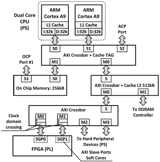
Figure 2.
The ZYNQ device architecture. The connection between programmable system (processors) and programmable logic (FPGA) parts.
To reach the FPGA fabric the data transfer request from the microprocessor is passed through three layers of AXI controllers. The microprocessor performs a single data item access cycle that does not take benefit from burst transfers offered by the AXI bus. A data exchange cycle is measured by the performance monitor unit. It uses an internal counter clocked with the elementary bus frequency of the local AXI controller. To make exact measurements the data exchange block has been programmed using inlined assembly language. The clock signal frequency influence on the AXI interconnection system performance has been evaluated for two frequencies. For the FPGA part, the 100 MHz and 200 MHz were used while the ARM processor core operated with 200 MHz and 600 MHz.
Table 1 gathers the interface cycles completion time for data read and data write issued by the processor to the peripheral device implemented in FPGA. The interface cycle duration is given using clock cycles (relative timing) and recalculated to time using clock frequency. It should be noted that the high-performance computing system due to its hierarchical architecture requires a relatively long time for accessing the input-output system. It should be noted that pooling the input-output device reduces sampling performance to 90 ns in the best case and 240 ns in the worst case. The data exchange cycle (read cycle followed by a write cycle) takes from 135 ns up to 510 ns in the worst case. Those properties of the interconnection system significantly influence the response time of the system. The elementary event that can be directly observed from the processing system depending on the frequency proportion between the processor and FPGA part must be longer than 90 ns (in the worst case 240 ns). The system reaction time to an event is no shorter than 225 ns in the best case. Shown system properties require designing an interface of a control system that manages time dependencies of a control cycle while software processing is called on the request of the interface system to relax the available time requirements of software processing.

Table 1.
The AXI crossbar performance for data transfer between CPU and FPGA fabric.
3. Controller Implementation Concept
The PMSM controller implementation block diagram is shown in case A of Figure 3. The controller is partitioned into interface system logic and controller computation part. The AXI bridge is a boundary between hardware and software. The interface system logic creates a tightly connected set of hardware peripheral components that implement input and output signals translation for the control algorithm. The input path implements a processing unit R2S (Rotating to Static) that transforms the winding currents of the tri-phase system into static vectors. The inverse transformation is performed in the output path by the S2R (Static to Rotating) computation unit. The S2R module delivers duty factors for the PWN controller for each phase of the inverter. It assures an appropriate relationship between the activity time of transistors separated by dead time gaps. The PWM controller determines the elementary computation cycle using the SYNC signal for initializing input signals acquisition. The windings current is averaged over the elementary period of the inverter using oversampling. This allows for the suppression of switching disturbances of the inverter. The motor shaft angle measurement (SHA) is placed at the end of the operation cycle allowing for obtaining the recent position for measured currents. Finally obtained results are passed to R2S processing and made available along with the activation of the IRQ line. This requests the software-based processing by calling the PMSM interrupt service. The time window for completing computation is almost equal to the inverter’s basic period (125 µs). The software processing results are collected from registers and passed to the S2R processing block. At the same time, the IGBT driver block starts the driving period with a dead time gap. Only 12 clock cycles are required for completing the computations by the S2R unit and delivering driving values for the inverter. The computation cycles of the S2R unit are hidden behind the dead time gap. In the considered implementation, the minimal dead time assuring correct operation is 120 ns while typically it is around several µs [12].
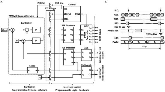
Figure 3.
The block diagram of the hardware-software based controller implemented using ZYNQ programmable system on chip (A) and its operation schedule (B).
The controller operation schedule is shown in case B of Figure 3. The waveform depicts the sequence of operations in a single control cycle. On the top is placed a SYNC/IRQ signal that triggers a new computation cycle. Listed resources are placed in the order of data flow. In the diagram are shown hardware components operations in control cycle time and software part procedure execution window.
4. Controller Interface System Implementation Details
The controller interface system assures precise input-output operations scheduling with relaxed timing requirements for software processing. The following subsections give architecture details and discuss the implementation efficiency of processing methods.
4.1. The PWM and Timing Controller Block
The FPGA device enables the implementation of a complex pulse width modulation system that integrates the synchronous operation of the tri-phase inverter driver system. The simplified block diagram of the synchronization unit and PWM modulator channel is shown in case A of Figure 4. The functional waveforms that illustrate the operations in the control cycle period are shown in case B of Figure 4.

Figure 4.
The PWM controller block diagram (A) and simplified operation waveform (B).
The PWM controller is responsible for synchronizing all computation processes of the controller. In the implementation, the 125 µs fundamental period is chosen. The TP counter generates a SYNC pulse every 12,500 clock cycles (fCLK = 100 MHz) which is determined by the TPER signal.
The PWM channel duty factor is controlled by the TD signal only. Based on its numeric value is generated a pulse on THx output and its complement on TLx output. The activities of outputs are separated by dead time periods of TOFF duration. The signals activity time expressed in clock cycles are as follows:
where: tH is the activity time of the THx output while tL is the activity time of TLx output for given settings of TD, TPER and TOFF, TCLK is the period of the clock signal.
The hardware implementation of the PWM assures the generation of all timing dependencies between signals necessary for the correct driving of the IGBT bridge. The crucial is assuring an appropriate time gap between active periods of opposite transistors that protects an expensive power element against accidental damage. To avoid an accidental modification of the dead time value (TOFF), it is implemented directly in the hardware structure and can be modified by resynthesizing the PWM module.
4.2. The Windings Current Sesning Unit
The winding current is measured in every period of the PWM inverter operation along with the measurement of the motor shaft position. Those values must be obtained in a correlated manner to assure correct computations of id and iq current values for the control algorithm. Switching transistors of the inverter are sources of significant disturbances influencing the momentary value of the current. Even though the passive filtering circuits are implemented in the power lines of the inverter, measured current signals are strongly distorted by the switching activity of transistors. Exemplary oscillograms of current sensors output are shown in Figure 5. The directly sampled signal is shown in case A It contains significant noise components from the working inverter. The noise can be eliminated through averaging, as case B illustrates. The square waveform at the bottom is the most significant bit of the angle converter used for synchronization purposes.
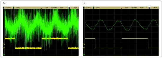
Figure 5.
Oscillograms of winding current signal from LEM sensors obtained directly (A) and with 64 samples averaging (B).
Using a compensation analog to digital converter a momentary value of the signal is captured and converted to a number. This method introduces a high error of measurement signals with periodic noise. Using an analog filter in the input signal path introduces the phase shift that results in the incorrect computation of static coordinate system values of id and iq in reference to the shaft angle. To get a usable signal appropriate filtering must be applied. The measurement process must be averaged in the period of inverter operation. This can be implemented as collecting an equally spaced sequence of samples for the period of inverter operation:
where: iw is a sum of n winding current samples i(…) over the inverter operation period, TINV—inverter period, t0—sampling start time. The iw is proportional to the average signal with a factor of n. The averaging measurement unit implementation requires synchronization of the sampling process to the inverter operation.
The ZYNQ device is equipped with a compensation analog to digital converter [19]. It can achieve the sampling performance of 1 Ms/s. The exact performance is slightly lower at 100 MHz clock, while the conversion takes 104 clock cycles. The converter performance is enough to take 64 samples over a 125 µs inverter basic period. The block diagram of the averaging integrated converter is shown in Figure 6. The XADC control is completely synchronized with the inverter operation. A set of samples is collected upon request pulse of the RQ signal. The value of collected signal samples is accumulated since the beginning of the measurement cycle as shown by (2).
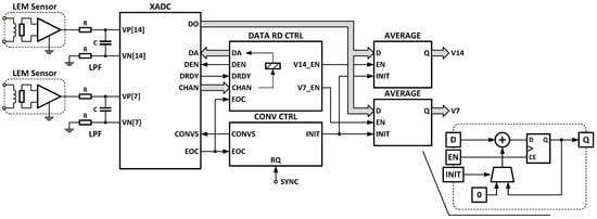
Figure 6.
Windings current measurement unit based on integrated XADC.
The measurement timing waveforms are shown in Figure 7. The implementation utilizes two ADC channels that are alternatively selected by the control unit to assure uniform distribution of measurement points in both current measurement channels. The distance of samples is 192 clock cycles. In total, 32 samples are collected for input current for each channel during one period of operation.
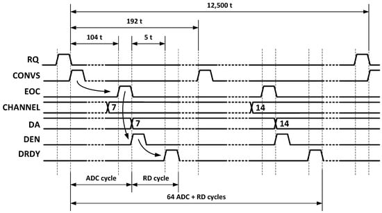
Figure 7.
Current measurement cycle timing.
The winding currents obtained using the proposed averaging method and acquired shaft angle are shown in Figure 8. Comparing oscillograms from Figure 5 and winding currents there could be observed switching noise elimination. The method can be compared to dual integration voltmeters where the input signal measurement is done over the period (or its integer multiplicity) of the disturbing signal. This results in eliminating the noises coming from the inverter’s IGBT switching.
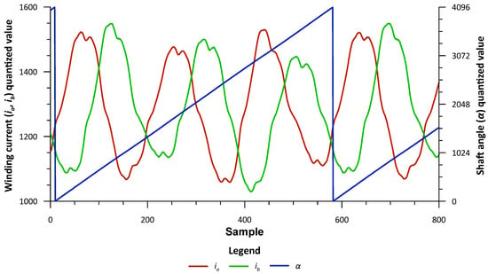
Figure 8.
Windings current captured by XADC using inverter period averaging and shaft angle acquired from MAB sensor.
4.3. The Vector System Processing Units S2R and R2S
The vector processing system consists of two transformation modules. The input path performs a transformation of the rotating input system of windings currents [ia, ib, ic] to static vectors [id, iq]. Initially, the tri-phase system is converted into two vectors [iα, iβ]
Next, the rotation of the [iα, iβ] with the angle α of shaft position is calculated to project vectors on [id, iq]:
The inverse transformation is based on computing tri-phase system voltages [Va, Vb, Vc] from [Vd, Vq] and the current motor shaft position α. First, voltage vectors from the static system are projected to rotating vectors [Vα, Vβ]:
Next, rotating vectors are projected to individual driving vectors of the inverter
There is also required post-processing of the vectors that shifts the vector from the signed range to the unsigned range of PWM space and assure value saturation in the range of correct operation of the PWM:
Outlined above theoretical background of the computations to perform allow moving to the implementation stage. The essential part of both transformations is the rotation of the vectors in two-dimensional space (4) (5). This operation requires computing sine and cosine functions of α angle. This task is complex and usually is implemented using floating-point computation (e.g., C math library) [20]. This introduces significant complexity and results in a long computation time. The coordinate rotation procedure should be accommodated to the resolution of angle measurement in the system that is represented by a 12-bit value. The precision of computations offered by a standard 32-bit floating point representation (IEEE 754) with 24-bit mantissa gives a 12-bit of computation precision margin.
Computing vector rotation can be considered a complete computation problem using the CORDIC approach [21]. The CORDIC algorithm is based on an iterative compensation-based approach. Step-by-step computations quickly converge to desired angle value. The computations in general can be put down as multiple vector rotations for the angle that arcus tangent is the power of 2 with a negative integer exponent {0, −1, −2,…}. The direction of the rotation is chosen based on the sign of the angle value from the previous computation step:
Putting down the rotation matrix and dividing it by cos we get:
Assuming that in each step the tangent value is selected as the ki factor above equation can be put down as follows:
The CORDIC method utilizes the addition and division by an integer power of two. In digital systems utilizing binary numbers division by a power of two is implemented as a shift-right operation. The final result requires scaling by the factor depending on step number:
The rotation process of the point for a given angle is calculated using conditionally selected addition or subtraction and shift operation as shown in (8)–(11). In a considered implementation, the final scaling can be omitted while values are used in the control loop with negative feedback. The adjustment multiplication can be assumed as a gain factor of the current sensor path or inverter voltage selection.
The computation procedure is well mapped into systolic array implementation that block diagram is shown in Figure 9. Computations can be implemented as an iterative structure that implies reduced requirements of hardware resources. The hardware resource reduction can be roughly estimated around the n (number of stages) to systolic implementation but some specific problems should be analyzed. The iterative implementation requires programmable shifters for xi and yi. A barrel shifter utilizing analogue switches [22] is implemented in ASICs. In FPGA devices the multiplexer-based structure consumes a large number of programmable resources. There is also an alternative of using a combinational multiplier block for shifting. The low resource count implementation is a shift register with the parallel load. This concept results in a significant extension of computation time. Additional clock cycles required for shift operations are a sum of the arithmetic sequence from 1 to n with a step of 1.
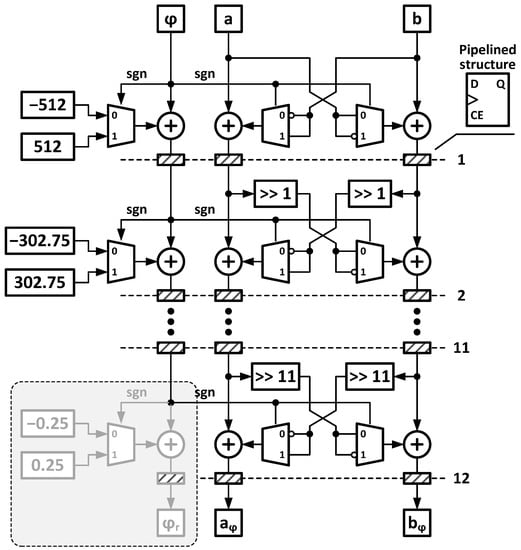
Figure 9.
The coordinates rotation computation unit based on CORDIC algorithm.
The systolic structure can be implemented as a pure combinational path (eliminating intermediate registers in Figure 9) or pipelined structure. The combinational implementation requires including wait cycles between arguments passing and obtaining the result while pipelined implementation offers the ability to achieve high clock frequency and average computation performance of one result per clock cycle.
It is essential to determine the number of steps required for computing the results with satisfactory precision. In the considered case the position sensor delivers an angle with a precision of 12 bits [15]. The number of iterations depends on the precision of the angle determination and can be calculated from following inequality:
where: k is the number of bits of angle sensor and n is the number of iterations for the CORDIC method to compute results with the required precision. Solving the precision inequality for the 12-bit shaft angle sensor number of iteration should be no less than 12. This constitutes the unit’s requirements for 12 systolic layers and a computation time of 13 clock cycles (including the input capture cycle) for pipelined architecture.
The CORDIC unit (as shown in Figure 9) allows the implementation of vector rotation only. Additional computations must be implemented separately. Since Xilinx Virtex II-PRO (high-end FPGA family) and Spartan 3 (budget FPGA family) multipliers are available in FPGA structures as dedicated hardware blocks. This allows for saving a lot of logic resources and achieving significantly better performance when multiplication is performed. For this reason, the implementation of vector rotation directly (either in the case of (4) or (5)) could be easily embedded into the preprocessing of winding currents and postprocessing of inverter voltages (PWM duty factors).
The essential problem is the fast computation of the sine and cosine of the shaft position angle. This method should compute results quickly and with the required precision of 12-bit angle encoding. The only way to get the result as quickly as possible is to use the lookup table approach. The implementation requires remembering three functions that are {sin(φ), cos(φ), and –sin(φ)}. There arises a question of implementation nature. Do we have to implement all three functions separately?
The first feature exploited in implementation is function symmetry. It is enough to remember only sin(φ) samples in the closed range . The remaining part of the function is restored by symmetry. When the period of the function is divided into equally spaced intervals the lookup table must store samples. This requires nonstandard implementation of the memory module with an odd number of cells and specific decoding circuitry.
The problem is overcome in the proposed implementation shown in Figure 10 by storing the sine function samples in the range (case B–black line). This allows the reduction of memory requirements only by half but eliminates the problem of additional hardware necessary for accessing the odd number of memory cells. Case A of Figure 10 illustrates the implementation of a universal sine and cosine function generator. The hatched rectangles denote the registers in the signal paths. The implementation with the required angle resolution is possible using the RAMB36 module [23] which can hold 2048 18-bit words. The output of the lookup table is passed to an adder that depending on the value of the MSB of the angle complements or passes simple content of the memory cell. In order to balance the registered delay of the memory block the register is placed on the A11 line to synchronize it with data arriving from the memory. In order to use the same lookup table for obtaining the sine and cosine functions the indexed addressing concept is used. The function selector (sel input) is considered as a two-bit offset added to the high-order bits of the angle φ. This two-bit vector when considered as the natural number introduces an angle shift inside the address word: .

Figure 10.
The block diagram of trigonometric functions sine and cosine fast computation module using RAMB36 lookup method (A) and operation concept (B).
This simple and fast function generator is only a part of the rotation computation unit. The computation system must implement equations (3)–(4) or (5)–(7) or both at once enabling separated calculations. When implementation of the unit is made the remaining calculations should be implemented to create the complete processing solution. The following will be illustrated the implementation of rotation to a static (R2S) computation core. The processing problem is illustrated using the data flow graph shown in case A of Figure 11. It could be observed that a similar sum of products is computed three times. To achieve high clock frequency the implementation should shorten the combinational paths and separate them with registers. Such architecture enables the introduction of a pipelined (overlapped) operation. Based on earlier authors’ experience and developed mapping methodologies [7] the developed data path block diagram is shown in case B of Figure 11. The modern FPGAs implement the DSP block that integrates a multiplier followed by an adder. In the case of Xilinx’s ZYNQ family, the DSP block is named DSP48E1 [24]. Such a structure is perfectly suited to implement multiply and accumulate (or pipelined add). Fitting computations into the DSP48E1 block allows for reducing the requirements for general-purpose logic resources and obtaining the processing system with short propagation delays that reflect the possibility of increasing the clock frequency.

Figure 11.
The R2S computation engine data flow graph (A) and hardware mapping using DSP48E1 and TrigCalc units (B).
It is essential to illustrate the performance and logic requirements of the proposed processing system in reference to other possible implementations that justify the selection. It is also important to compare the hardware implementations with pure software-based computations. Table 2 gathers the performance factors of different implementations. The two first rows collect the programmatic implementation of rotations using ARM Cortex A9 running at 600 MHz and compiled with speed optimization [20]. The first one (Trig. Rotation) utilizes the math library and floating point implementation. Even though ARM supports floating point instructions computing a single rotation requires 3.83 µs. An improvement is observed for the CORDIC sw (abbreviation of software) implementation utilizing integers for number representation. In this implementation, computation time has been reduced to 37.7% of the initial time and requires 1.445 µs.

Table 2.
Comparison of computation execution time and resource requirements depending on implementation method–programmatic or direct hardware implementation.
The next five implementations are dedicated to the programmable hardware platform. It is assumed that the hardware platform is clocked with a frequency of 100 MHz. First, the CORDIC implementation is examined. The benefit of this implementation enables getting rotation results of both coordinates in a single computation process. The first implementation utilizes the combinational structure. Registers are placed on the processing system inputs and outputs only enabling free data flow through the structure. In this case, the rotation is computed in 30 ns (3 clock cycles). There is an observed long propagation delay in the circuit path that requires two clock cycles to completely propagate the data (propagation delay of 14.8 ns). This is illustrated by the maximal clock frequency of 67.8 MHz. The CORDIC pipe implementation shows changes in performance when all stages are separated with registers. The computations take 130 ns (13 clock cycles). It should be observed that the pipelined structure offers the maximal performance of average computations of one clock cycle per sample. In the considered case the deep pipelined structure (12 stages) is not required while only one computation is done for a sample.
Next, implementation is based on the computation of sine and cosine using the lookup table approach. The performance of the sine and cosine computation unit based on RAMB memory used as a lookup table is shown first to give the reference point. There should be observed minimal resource requirements for computing. When compared with CORDIC implementations the LUTs requirement has been reduced 33.7 times (from 641 to 19). The lookup table based architecture offers an extremely high clocking frequency of more than 600 MHz and pipelined operation. Using a pipelined architecture enables completing the computations of sine and cosine functions in 6 clock cycles that improve the performance of the following implementations of R2S and S2R units. Finally, coordinate system computation units are presented. Its implementation utilizes the lookup table-based sine and cosine computation unit. The data flow diagram shown in Figure 11 perfectly fits the DSP48E1 unit computing capabilities. It should be noted that such a unit is located next to the RAMB32 block. The close location of components reduces programmable connection length allowing for high-frequency operation. The total computation time of R2S is 12 clock cycles while reverse computations in S2R blocks take 14 clock cycles. In comparison to CORDIC pipe implementation, the computation time is comparable. There is a wide margin between maximal and operating frequency (requested 100 MHz, the worst achieved case is 266.5 MHz for S2R). The peripheral frequency can be set to 250 MHz meeting timing requirements, which is the maximal frequency of PLL for peripheral clocking [11]. The CORDIC implementation enables the illustration of resource requirements reduction and architecture fitting. The R2S requires about 8.4 times fewer general-purpose logic resources while the S2R ratio is about 4.42. It should be noted that the CORDIC algorithm is only a part of the computations to be implemented while remaining the transformations between 3-phase and two vectors systems that require general-purpose resources and additional computation time.
4.4. The Controller Interface Implementation Summary
Processing blocks that are shown as separate units are put together creating a complete input-output system for the ZYNQ device shown in Figure 3. The synthesis results for separate modules and the complete interface unit are gathered in Table 3. There are listed resource requirements for specific types and the maximal clocking frequency for each unit. Finally, it is summarized with the complete system implementation in the last row. Results are obtained using Vivado synthesis and implementation toolset [25].

Table 3.
Resource requirements and performance of elementary components and complete interface system for PMSM control implemented in XC7Z010.
Processing blocks resources consumption is relatively low in comparison to CORDIC processing core implementation (641 LUTs and up to 542 flip-flops Table 2). The high maximal frequencies are achieved by reducing the number of logic layers between registers. The modules architecture utilizes pipelined approach for arithmetic processing systems and utilizes dedicated DSP48E1 cores for multiplication and addition operating in pipelined fashion by separating the multiplier and the 48-bit accumulator with registers (Figure 11, case B) [24]. It is worth pointing out that even though the R2S and S2R are implemented as independent units they share the same sine lookup table implemented using RAMB32 memory operating in dual port mode [23] as seen in Table 3 in PMSM_AXI row. The maximal operating frequency of the input-output system assures a wide margin of clocking to the requested operating frequency of 100 MHz. The AXI interconnect system equipped with diagnostic ports requires 27.6% of total LUT resources and 13.1% of the total flip-flops number. The maximal frequency drop is less than 0.37%. There is observed minimal influence of integrating the controller and attaching the AXI interface to it.
5. Conclusions
Presented in the paper implementation of the PMSM controller allows for precise controlling of the inverter and collecting current shaft position and winding currents. This was achieved by developing a dedicated input-output system that synchronizes all operations. There has been used fixed-point arithmetic in place of floating point implementation which is resources and time demanding in hardware implementation. Along with precise control, there is offered significant loosening of time requirements and implementation simplification for control computation using a programmatic platform. The control can be executed in a relatively long time window of the elementary cycle of the controller operation. Computed results that are delivered at any time of the processing window are precisely applied at desired moments of the computation window. This allows for eliminating the time uncertainty caused by variable execution time of a program and long access times to input-output system caused by multiple layers of AXI interconnection system.
The hardware interface also implements all signal transformations that are independent of the high-level control algorithm. This pre and post-processing are efficiently calculated using scheduling and mapping methods that enable the use of DSP48 processing cores and RAMB32 dual port memory. Appropriate selection of algorithm implementation and careful operation scheduling allows for reduce of general-purpose logic resource requirements and achieves high computation throughput. Developed controller architecture can be applied in a wide range of power electronic applications utilizing inverter driving combined with high-level algorithmic control. Further works concentrating on control application development and testing our PMSM motor stand and advanced control of power inverters applications.
Author Contributions
Conceptualization T.R., A.M.; Implementation methodology A.M.; Implementation T.R., A.M.; Validation T.R., A.M.; Manuscript preparation A.M.; Manuscript revision T.R., A.M. All authors have read and agreed to the published version of the manuscript.
Funding
This work was supported by funding from the Ministry of Science and Higher Education for Statutory Activities of Digital Systems Division of the Silesian University of Technology of Gliwice (BK247/RAu-12/2022).
Institutional Review Board Statement
Not applicable.
Informed Consent Statement
Not applicable.
Data Availability Statement
Not applicable.
Conflicts of Interest
The authors declare no conflict of interest.
References
- Krishnan, R. Permanent Magnet Synchronous and Brushless DC Motor Drives, 1st ed.; CRC Press: Boca Raton, FL, USA, 2010. [Google Scholar] [CrossRef]
- Yang, Z.; Shang, F.; Brown, I.P.; Krishnamurthy, M. Comparative Study of Interior Permanent Magnet, Induction, and Switched Reluctance Motor Drives for EV and HEV Applications. IEEE Trans. Transp. Electrif. 2015, 1, 245–254. [Google Scholar] [CrossRef]
- Baek, S.-W.; Lee, S.W. Design Optimization and Experimental Verification of Permanent Magnet Synchronous Motor Used in Electric Compressors in Electric Vehicles. Appl. Sci. 2020, 10, 3235. [Google Scholar] [CrossRef]
- Bernacki, K.; Rymarski, Z. A Contemporary Design Process for Single-Phase Voltage Source Inverter Control Systems. Sensors 2022, 22, 7211. [Google Scholar] [CrossRef]
- Thiele, L.; Wilhelm, R. Design for Timing Predictability. Real-Time Syst. 2004, 28, 157–177. [Google Scholar] [CrossRef]
- Wisniewski, R.; Bazydlo, G.; Szczesniak, P. Low-Cost FPGA Hardware Implementation of Matrix Converter Switch Control. IEEE Trans. Circuits Syst. II Express Briefs 2018, 66, 1177–1181. [Google Scholar] [CrossRef]
- Milik, A.; Kubica, M.; Kania, D. Reconfigurable Logic Controller—Direct FPGA Synthesis Approach. Appl. Sci. 2021, 11, 8515. [Google Scholar] [CrossRef]
- Wiśniewski, R. Prototyping of Concurrent Control Systems Implemented in FPGA Devices; Springer: Berlin/Heidelberg, Germany, 2017. [Google Scholar]
- Monmasson, E.; Cirstea, M.N. FPGA Design Methodology for Industrial Control Systems—A Review. IEEE Trans. Ind. Electron. 2007, 54, 1824–1842. [Google Scholar] [CrossRef]
- He, L.; Wang, F.; Wang, J.; Rodriguez, J. Zynq Implemented Luenberger Disturbance Observer Based Predictive Control Scheme for PMSM Drives. IEEE Trans. Power Electron. 2019, 35, 1770–1778. [Google Scholar] [CrossRef]
- Xilinx: UG585: Zynq-7000 All Programmable SoC Technical Reference Manual, ver .1.13; Xilinx Inc.: San Jose, CA, USA, 2021.
- Mitsubishi Electric: Intelligent Power Modules—PM50RLA060. May 2005.
- Czerwinski, R.; Rudnicki, T. Examination of Electromagnetic Noises and Practical Operations of a PMSM Motor driven by a DSP and Controlled by means of Field Oriented Control. Elektron. Ir Elektrotechnika 2014, 20, 46–50. [Google Scholar] [CrossRef]
- Sung, G.-M.; Wu, P.-E.; Xu, J.-M. 10-Bit Successive Approximation Register Analog to Digital Converter for BLDC Motor Drive. In Proceedings of the International Symposium on Computer, Consumer and Control (IS3C), Taichung, Taiwan, 13–16 November 2020; pp. 224–227. [Google Scholar] [CrossRef]
- Megatron: Series MAB28 SER/Hall Effect Absolute Encoder, Datasheet. 2013.
- O’Rourke, C.J.; Qasim, M.M.; Overlin, M.R.; Kirtley, J.L. A Geometric Interpretation of Reference Frames and Transformations: dq0, Clarke, and Park. IEEE Trans. Energy Convers. 2019, 34, 2070–2083. [Google Scholar] [CrossRef]
- Patterson, D. Computer Organization and Design RISC-V Edition: The Hardware Software Interface; Morgan Kaufmann Publishers: Burlington, MA, USA, 2021. [Google Scholar]
- ARM: AMBA® AXI™ and ACE™ Protocol Specification, ARM. 2011.
- Xilinx: 7 Series FPGAs and Zynq-7000 All Programmable SoC XADC Dual 12-Bit 1 MSPS Analog-to-Digital Converter, UG480 ver 1.22; AMD Xilinx: San Jose, CA, USA, June 2022.
- Xilinx: Xilinx Software Development Kit (SDK) User Guide—System Performance Analysis, UG1145; Xilinx: San Jose, CA, USA, May 2019.
- Liu, Y.; Fan, L.; Ma, T. A Modified CORDIC FPGA Implementation for Wave Generation. Circuits Syst Signal Process 2014, 33, 321–329. [Google Scholar] [CrossRef]
- Abbas, K. Handbook of Digital CMOS Technology, Circuits, and Systems; Springer: Cham, Switzerland, 2020. [Google Scholar]
- Xilinx: 7 Series Memory Resources, UG473 ver. 1.14; Xilinx: San Jose, CA, USA, July 2019.
- Xilinx: 7 Series DSP48E1 Slice, UG479 ver 1.10; Xilinx: San Jose, CA, USA, March 2018.
- Xilinx: Vivado Design Suite User Guide. Implementation, UG904, ver. 2021.1; Xilinx: San Jose, CA, USA, August 2021.
Disclaimer/Publisher’s Note: The statements, opinions and data contained in all publications are solely those of the individual author(s) and contributor(s) and not of MDPI and/or the editor(s). MDPI and/or the editor(s) disclaim responsibility for any injury to people or property resulting from any ideas, methods, instructions or products referred to in the content. |
© 2023 by the authors. Licensee MDPI, Basel, Switzerland. This article is an open access article distributed under the terms and conditions of the Creative Commons Attribution (CC BY) license (https://creativecommons.org/licenses/by/4.0/).