Article

Multi-Layer QCA Shift Registers and Wiring Structure for LFSR in Stream Cipher with Low Energy Dissipation in Quantum Nanotechnology

Department of Convergence Science, Kongju National University, Gongju 32588, Republic of Korea
Electronics 2023, 12(19), 4093; https://doi.org/10.3390/electronics12194093
Submission received: 28 August 2023 / Revised: 21 September 2023 / Accepted: 27 September 2023 / Published: 29 September 2023
(This article belongs to the Special Issue Design of Low-Voltage and Low-Power Integrated Circuits)

Abstract

:
Pseudorandom numbers (PRN) are used in various cryptographic applications, such as cryptographic protocols and stream ciphers. The most efficient hardware method used to generate PRNs is to use a Linear Feedback Shift Register (LFSR) structure, which is generally composed of a Shift Register (SR) and an XOR gate. The most important factors in designing the entire LFSR structure are design cost and energy efficiency, which are highly dependent on the SR structure. In the proposed study, the structural characteristics and problems of existing various types of SRs are presented, and new multi-layered serial-in-serial-out (SISO) and parallel-in-parallel-out (PIPO) SRs are proposed. In addition, we compare and analyze the area-time complexity, design cost, and energy dissipation through simulation using QCADesigner and QCADesigner-E. As a result, the proposed SISO and PIPO showed a performance improvement of more than 27% compared to the existing structure, which showed the best performance, and showed energy dissipation reduction rates of about 65% and 59%, respectively. In particular, we proposed multi-layer wiring that can reduce energy dissipation and verified through simulation that it can save up to 24.8%.

1. Introduction

CMOS technology is reaching its physical limits with problems such as short-channel effects, interconnect delays, and high power consumption, and Moore’s Law has also reached its limit [1]. Quantum-Dot Cellular Automata (QCA) is a next-generation quantum circuit design technology that shows improved characteristics in terms of energy efficiency, operation speed, and area compared to previously used digital circuit design technologies. Due to these characteristics, it is considered that QCA can replace the digital circuit design technology represented by conventional CMOS [2,3,4].
Various existing digital circuits have been redesigned into QCA circuits. Most circuits have been designed and improved with an emphasis on reducing circuit area and latency [5,6,7]. In addition to this, research is being conducted to minimize the energy dissipation that occurs during circuit operation and fault tolerance [8,9,10,11,12]. In addition, although various studies are being conducted to improve the energy dissipation of the circuit, a specific method or model for minimizing it is currently not proposed. Most of the recent studies have been carried out in a way to reduce the overall energy loss by reducing the area of the circuit [13,14,15,16]. Currently, the best way to reduce the area is to implement circuits around the existing majority gate using cell interaction [17,18,19].
Existing studies have focused on the calculation part, which is the core of the circuit, and have hardly progressed on the energy loss of wiring, which is indispensable in constructing a circuit. Meanwhile, in this study, the hardware design of the pseudorandom number generator (PRNG), which is widely used in linear cryptography and cryptographic protocols, is mainly implemented by the linear feedback shift register (LFSR) structure. The core principle of stream ciphers is to generate ciphertext through XOR operations with the original text by generating a bit string or character string with a long period [8,20]. Therefore, since the LFSR structure with a long period consists of a long SR structure and a small number of XOR gates, most of the design cost and energy consumption are highly dependent on the SR structure. At this time, the SR is composed of D-latch or Mux [21,22,23,24,25,26,27].
The efficient design of the SR structure, which requires the largest area and latency in the components, is proportional to the efficiency of the entire LFSR structure. This has a high relationship with the energy dissipation rate, which directly affects signal stability and circuit operation. This study also identifies the wiring problem that arises as the number of bits increases in linear structures and determines how much energy consumption can be reduced by solving this problem.
The SR is classified into four types according to the input/output structure designed by function: serial-in parallel-out (SIPO), serial-in serial-out (SISO), parallel-in parallel-out (PIPO), and parallel-in serial-out (PISO) [28,29,30,31,32,33,34,35,36,37,38]. We would like to analyze and discuss three structures except for PISO, which is not often used due to structural reasons. The contributions of this study can be summarized as follows:
  • Multi-layered SISO and PIPO QCA circuits using cell interactions are proposed.
  • The structure, characteristics, and energy dissipation of SR structures are compared and analyzed.
  • Problems with existing SR structures are presented, and ways to increase signal stability through structural improvement are proposed.
  • A method for minimizing energy dissipation by changing the wiring structure is proposed.
  • The novelty of the proposed research is the easy conversion of serial and parallel input and output in a multi-layer structure and the proposal of a multi-layer wiring technique.
  • A modified equation that can calculate the design cost of a QCA circuit including a MUX using cell interaction is proposed.
  • The performance and energy dissipation of the proposed structures and existing circuits are simulated and compared using QCADesigner and QCADesigner-E.
This paper is structured as follows: In Section 2, the basic background knowledge of QCA and the existing SR structures is reviewed; in Section 3, we propose SISO and PIPO SRs; and in Section 4, the performance and energy dissipation of existing SRs and the proposed structures are compared and analyzed. In addition, a new wiring structure is proposed, and the relationship between the proposed wiring structure and energy dissipation rate is investigated. Finally, we conclude in Section 5.

2. Related Works

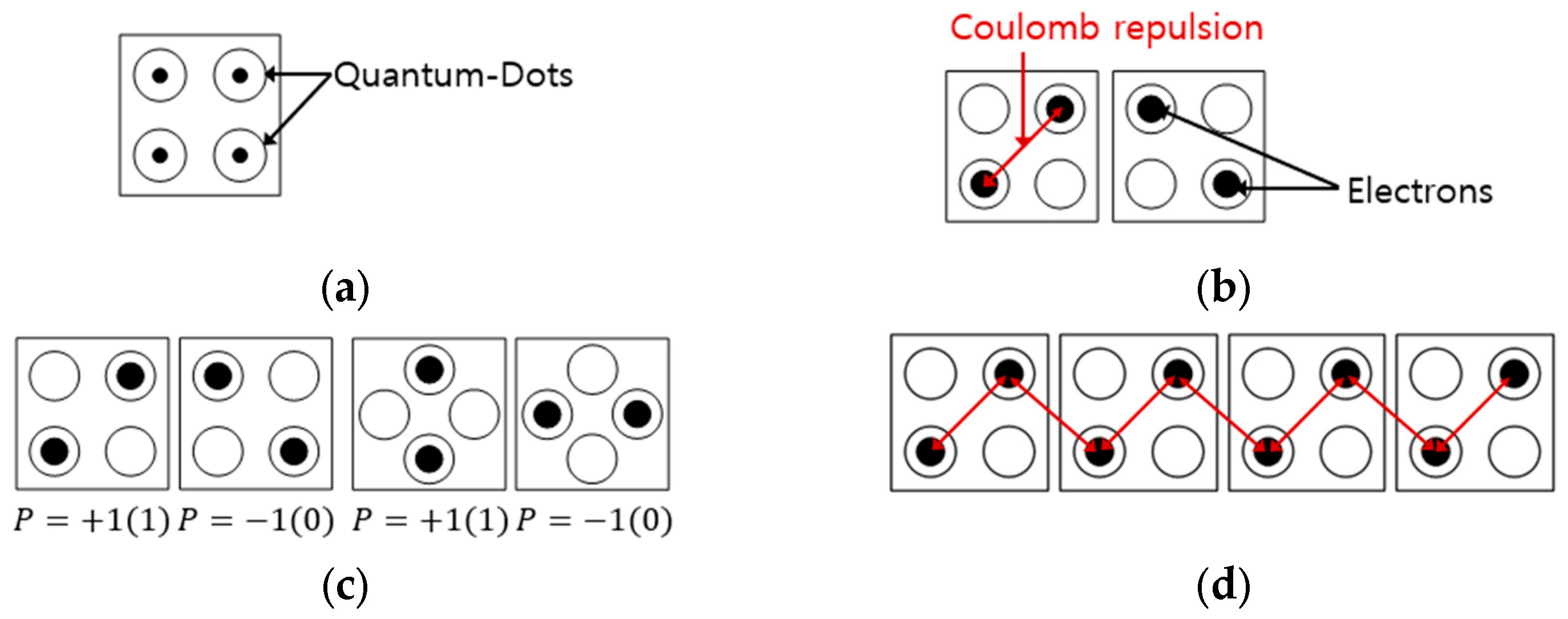
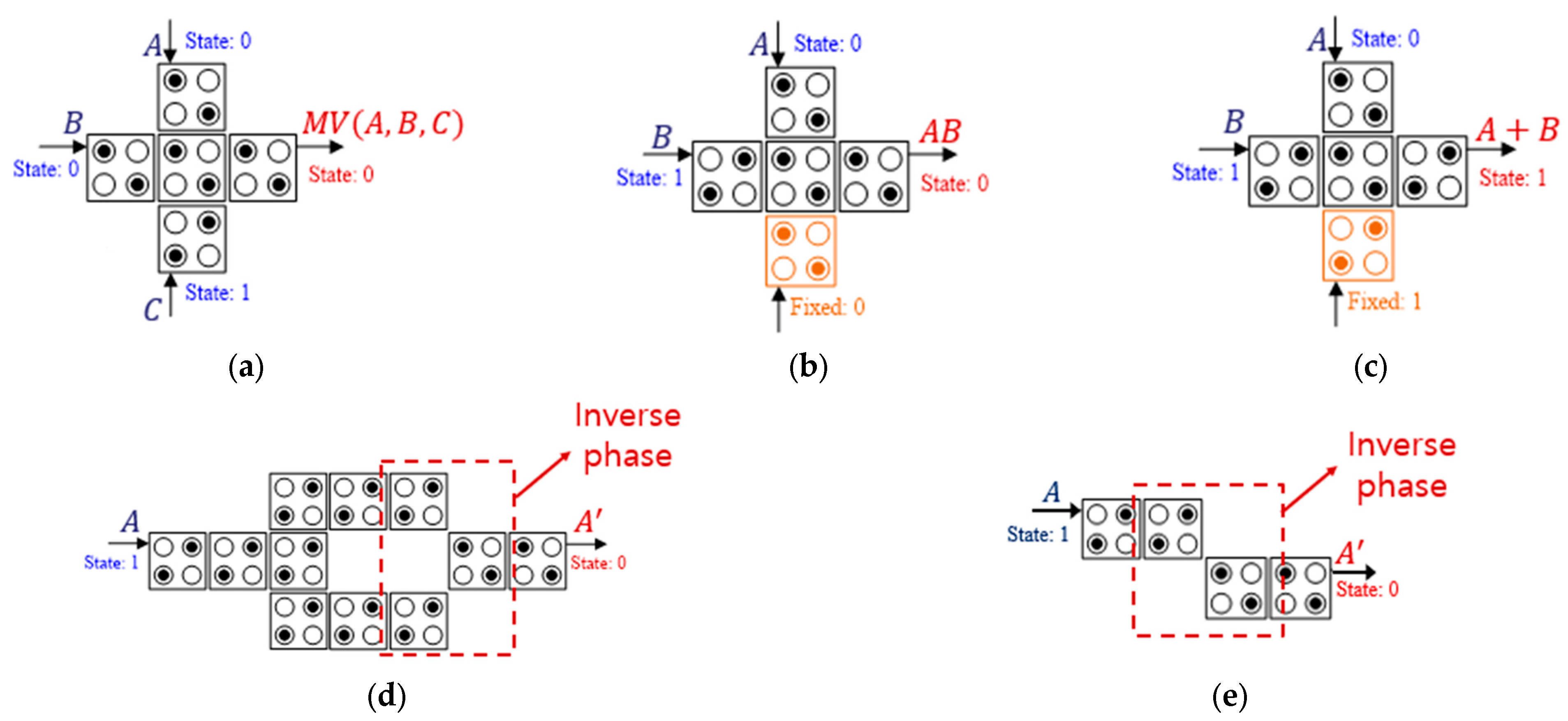
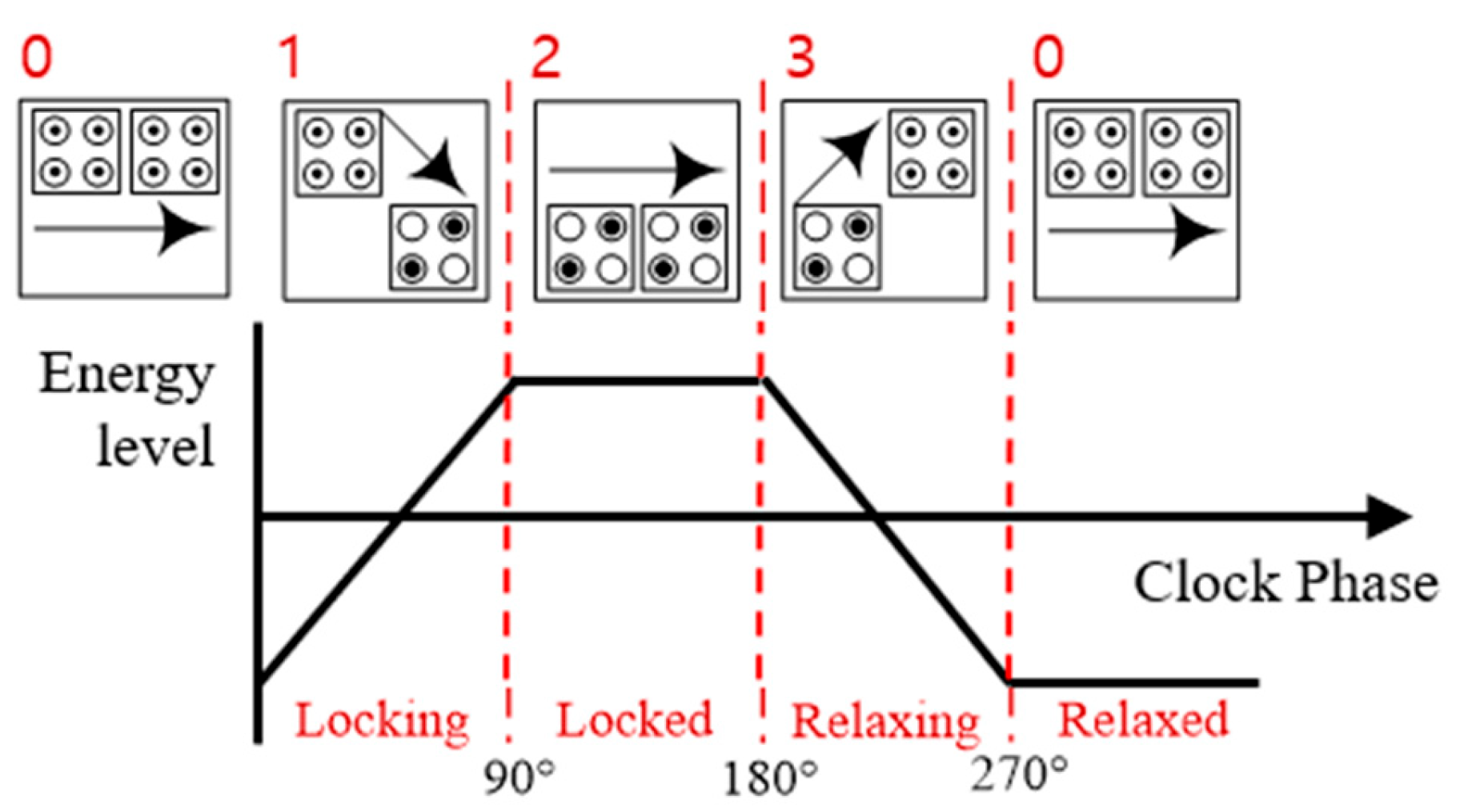
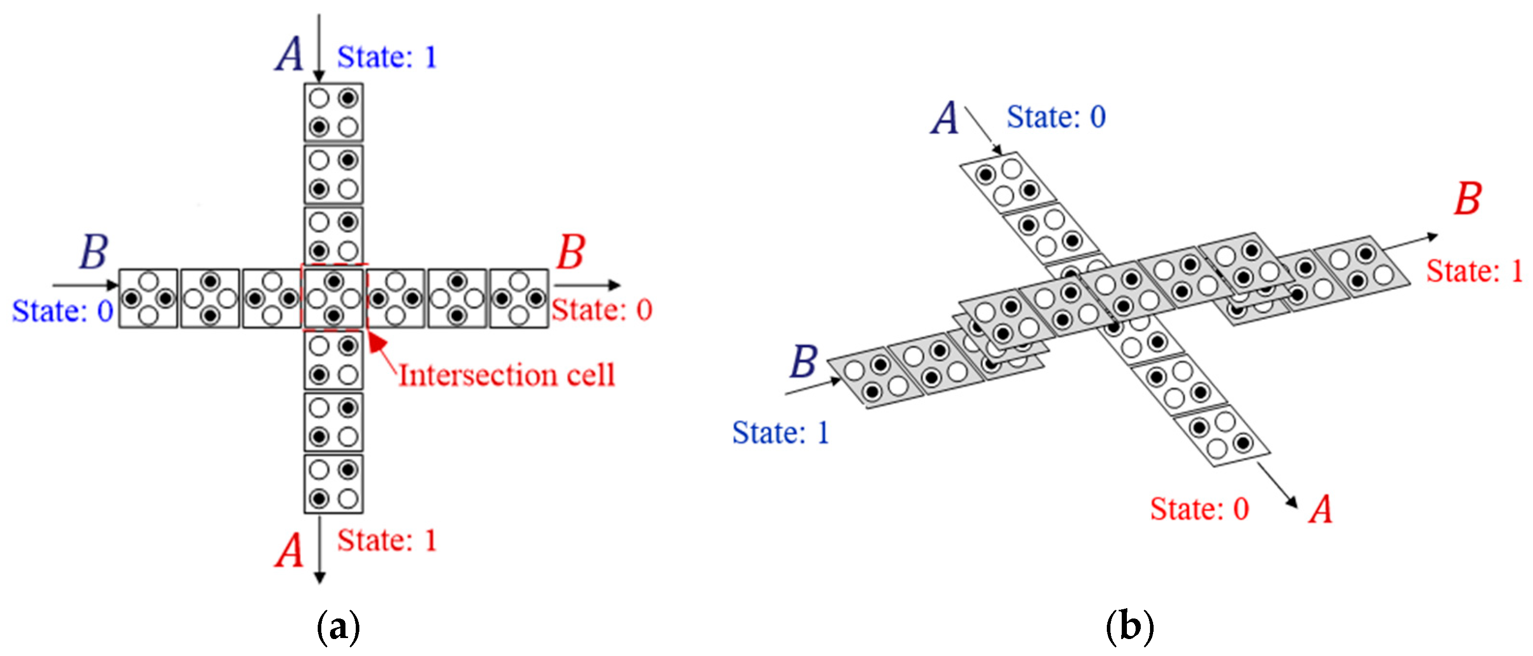
2.1. Background of QCA

One QCA cell is composed of four quantum dots in a square pattern. In addition, the QCA cell state can be divided into a null state in which electrons are not activated, as shown in Figure 1a, and a polarized state in which two electrons in each cell are activated, as shown in Figure 1b [1]. The two electrons have a repulsive force that pushes each other, and this is called Coulomb repulsion. Therefore, as shown in Figure 1c, two states are possible, and cell polarization P = +1 or −1 in standard cells and 45° rotated cells represents “1” or “0” in binary logic [2]. QCA wiring can be made most simply by attaching cells next to QCA cells in order.
M V A , B , C = A B + B C + A C
Figure 2a shows a majority vote (MV) gate to represent a logic gate. The logic function of the MV gate is achieved by Equation (1). Therefore, as shown in Figure 2b or Figure 2c, when the input value of C becomes 0 or 1, the MV gates perform AB or A + B operations. Therefore, it can be used as an AND or OR gate. Figure 2d,e show a strong and weak inverter, respectively. In the inverse phase, each state value is changed to the opposite value by the Coulomb repulsive force. Since the output value of a strong inverter is changed by the Coulomb repulsive force of two cells, the signal strength is stronger than that of a weak inverter that is changed by one cell, and the value is transmitted stably [5,6,7].
A QCA cell has four clock states. Locking is a period in which the potential of the cell gradually increases and becomes stronger, Locked is a state in which the potential between quantum dots is maintained high, Relaxing is a period in which the potential gradually decreases and becomes weak, and Relaxed means a state in which all potential is lost. In QCA, these four states constitute one clock cycle, and each clock phase has an interval delay of 90°. Figure 3 shows these four state changes along with clock changes from clock 0 to clock 3. The arrow inside the square box indicates the state change of the corresponding clock phase. These states are also called Switch, Hold, Release and Relax [2,3]. When an input value enters an input cell, neighboring cells are sequentially activated according to the clock state.
The QCA circuit is classified into a coplanar structure composed of only one layer and a multi-layer structure using several layers [19]. Unlike the coplanar structure, the multi-layer structure has a high design complexity because the circuit is designed considering the interaction between the layers. Figure 4a shows the wire crossover of the coplanar structure. Normal cells and cells rotated by 45° do not affect each other’s values when crossing, so they can be used for plane crossing. Figure 4b is a wire crossover of a multi-layer structure using three layers and shows that the value of the other layer is not affected when there is a difference between two or more layers [33,35].

2.2. Previous QCA SR Structure

A SR is a circuit that temporarily stores binary information in storage and transfers information left or right. The n-bit SR is composed of n D-latches and wires, and 1-bit binary information is input to the SR according to a clock input, and the stored information is shifted according to the next clock input. SRs are classified into four types according to the input/output format: SIPO, SISO, PIPO, and PISO. Figure 5 shows the logic diagram of the shift registers, excluding PISO, which is not frequently used.
Figure 6 shows various typical structures on SIPO SR. In 2015, Beigh et al. proposed a 3-bit SR to design a LFSR [28], and Reshi et al. introduced three types of SR [29]. In 2019, Roshan et al. proposed a 4-bit serial SR with a reset function and minimized complexity [30], and in 2021, Ajitha et al. proposed a SR using a 5-input MV gate [31], and Fan et al. proposed serial and parallel SR using a dual edge-triggered D flip-flop [32]. Recently, in 2022, Kim et al. proposed a multi-layered SIPO SR while proposing an LFSR structure for random number generation [33].
Figure 7 shows various typical SISO SRs. In 2015, Reshi et al. introduced three types of SR [29], and in 2017, Das et al. proposed a 3-bit SR under thermal randomness [34]. In 2018, Divshali et al. proposed a multi-layered SR consisting of three different D flip-flops and five layers [35], and Kalyan et al. proposed a 4-bit SR using a JK flip-flop [36]. In 2019, Abdullah-Al-Shaf et al. proposed a SIPO-type SISO SR with a RAM structure [37], and Li et al. proposed a SISO SR with PIPO [38].
Figure 8 shows the existing research on PIPO SR, where both input and output are made in parallel. In 2015, Reshi et al. introduced PIPO SR along with SIPO and SISO structures [29], and in 2019, Li et al. proposed PIPO SR together with SISO structures [38]. Moreover, in 2021, Fan et al. proposed serial and parallel SRs with dual edge-triggered D flip-flops [32].

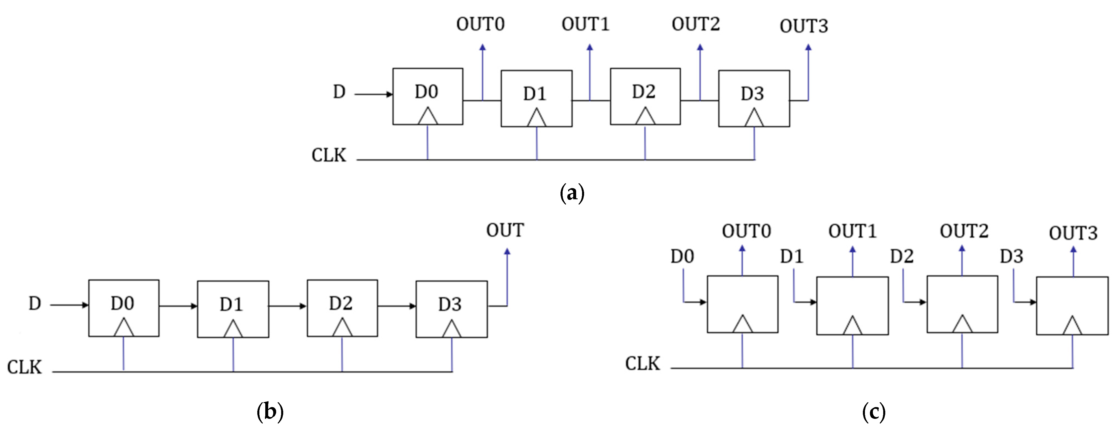
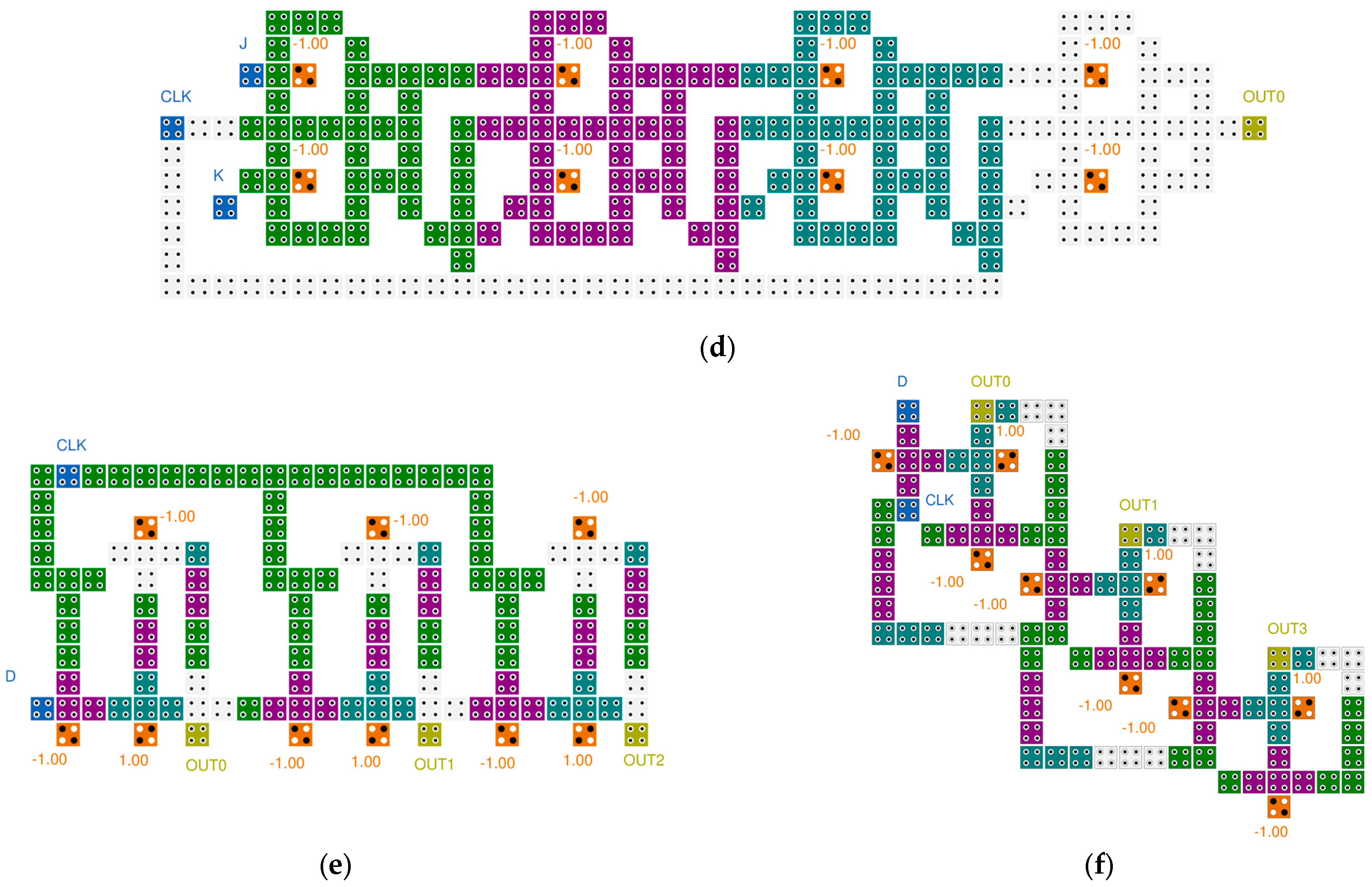
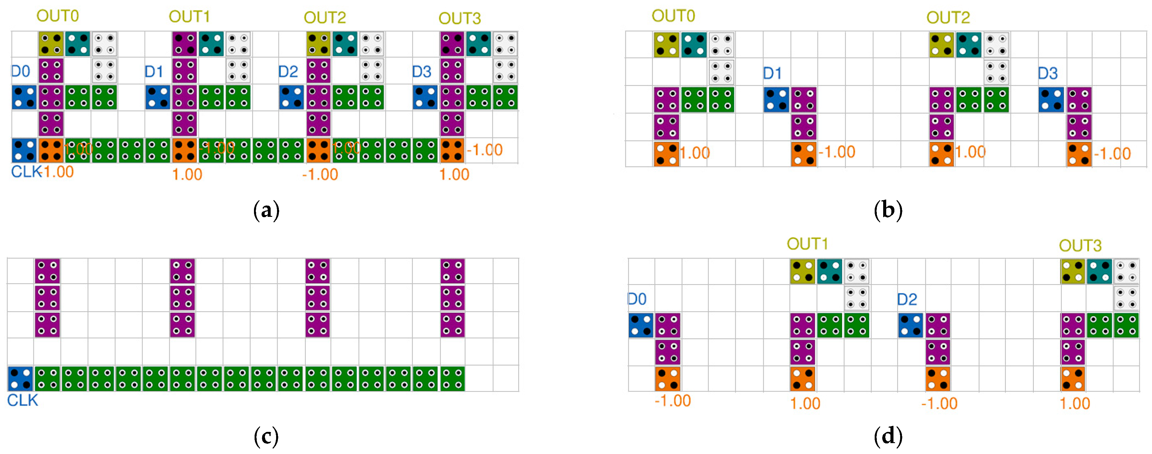
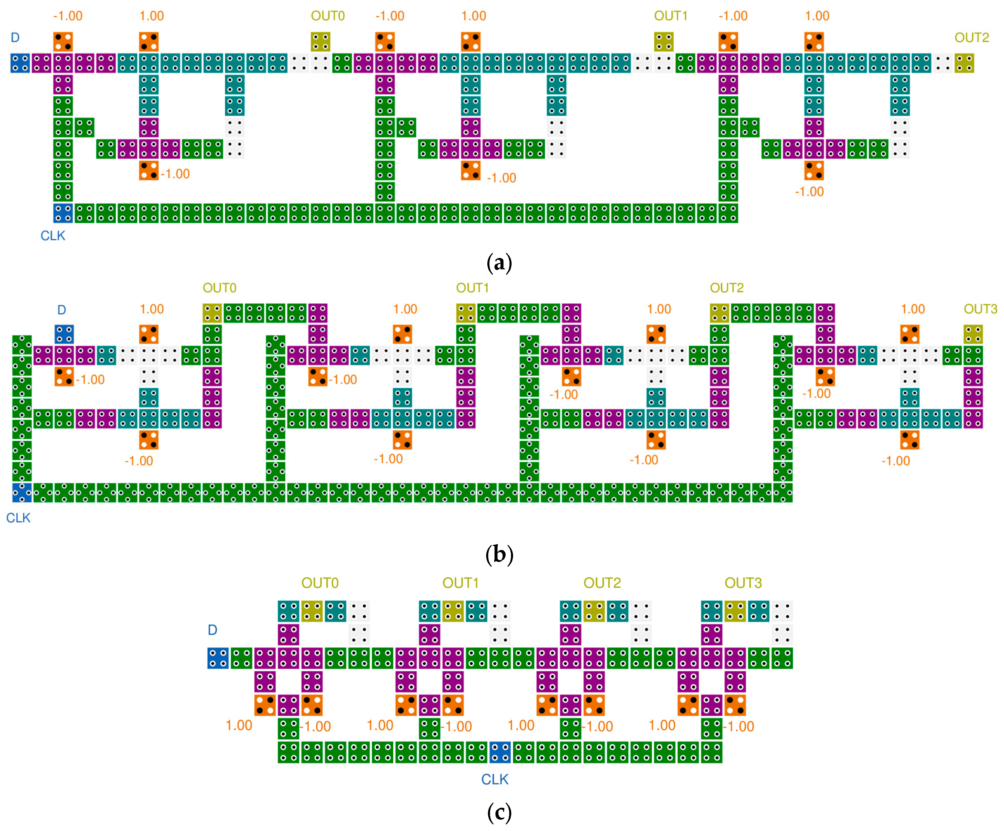
3. The Proposed Structures

In 2022, our team proposed a multi-layered D-latch to design an efficient LFSR structure and proposed a SIPO SR [33]. The proposed D-latch was designed very simply by cell interaction without using an MV gate. In this section, we show how easily the existing SIPO structure can be converted into SISO and PIPO structures and how superior the modularity and extensibility of the proposed structures are compared to the existing ones. Figure 9 shows a 4-bit SISO SR proposed in this study. The input value D is stored in the D-latch using the multi-layer structure and transmitted to the next D-latch by the CLK input. The proposed SISO SR can be easily implemented by replacing the output cells of layers 1 and 3 of the existing SIPO structure with normal cells.
Figure 10 shows a proposed 4-bit PIPO SR. For parallel input and output, input values D0~D3 and output values OUT0~OUT3 are located in all D-latch. Since each input cell is in a very stable state, it was confirmed that stable signal transmission is possible even though it is composed of only one cell. In addition, it was confirmed that each input value was output in parallel to the corresponding latch on every clock.
As shown in Figure 9 and Figure 10, the proposed SR structures can be converted very easily regardless of the type, and it can be confirmed that each layer of the proposed structure is easily expandable due to its excellent modularity. In addition, the structure using cell interaction does not depend on the operation of the MV gate.

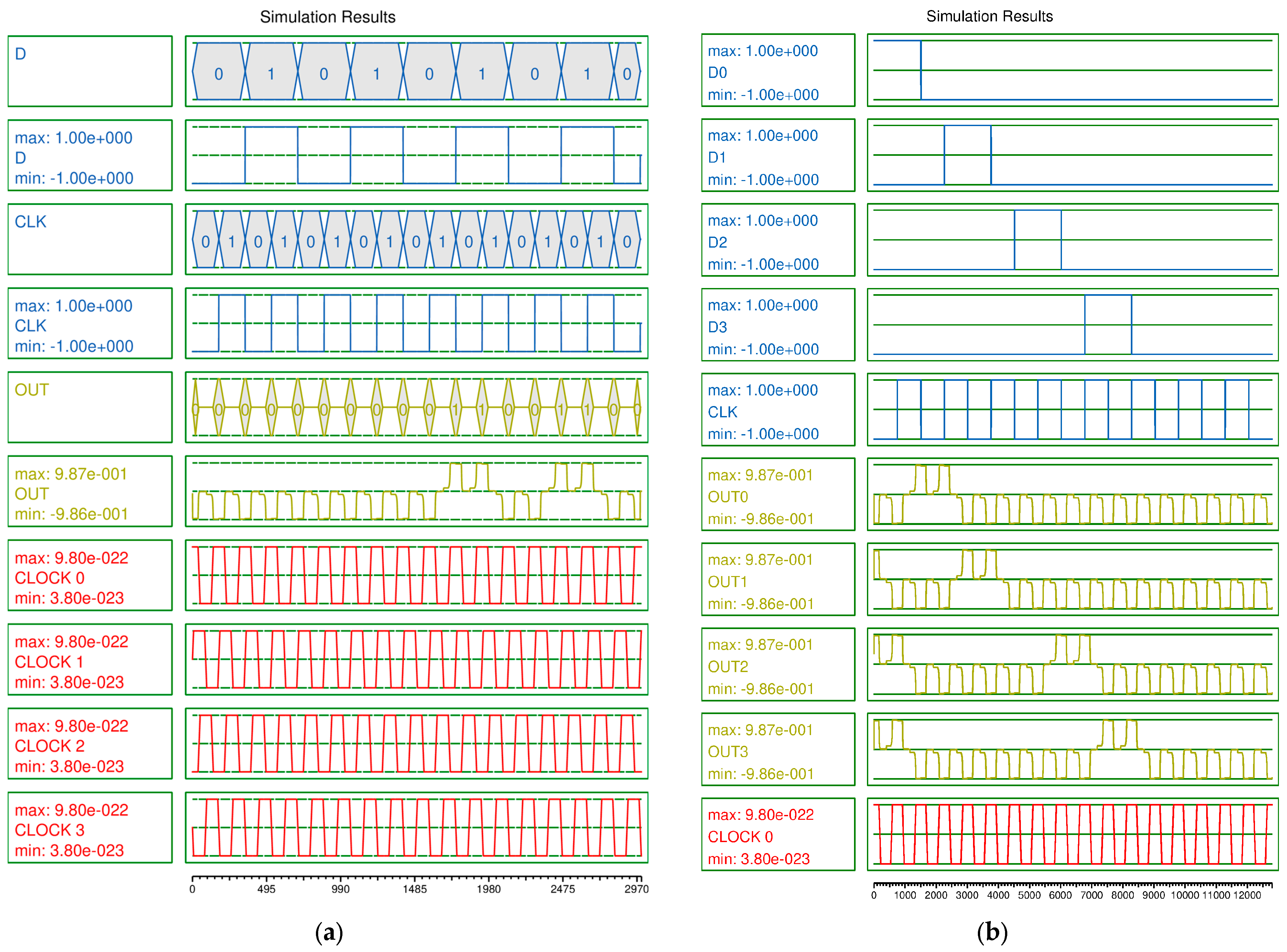
4. Structural Analysis and Simulation

In this section, we compare and analyze the performance along with the structural analysis of existing SR structures.

4.1. Structural Analysis

Since the LFSR structure for calculating a cryptographic random value only needs to add an XOR gate to the SR structure, most of the structure design cost depends on the SR structure. QCADesigner (version 2.0.3) was used to measure the design complexity of SR structures and to measure the accuracy and reliability of operations [39]. The simulation engine used Bistable Approximation, and the values of the simulation parameters are as follows: cell size: 18 nm, dot diameter: 5 nm, cell separation: 2 nm, layer separation: 11.5 nm, clock high: 9.8 × 10⁻²² J, clock low:3.8 × 10⁻²³ J, clock shift: 0, clock amplitude factor: 2.0, relative permittivity: 12.9, Temperature: 1 K, relaxation time: 1.0 × 10⁻¹⁵ s, time step: 1.0 × 10⁻¹⁶ s, and radius of effect: 65 nm.
The method of measuring the cost of QCA circuit design varies according to the basic unit and purpose of the circuit design [40]. There is a problem in that the existing cost measurement method for circuits designed based on MV gates cannot be applied to circuits based on cell interaction. Therefore, in this study, the design cost is calculated using the most basic AT product and the newly proposed cost calculation formula. AT complexity using the product of circuit area and latency is defined as Equation (2).
A T   c o m p l e x i t y = A × T p , 0 p 2
where A is the area and T is the latency of the QCA circuit. We assume that the value of p is 1 here and calculate and compare the AT complexity for each bit. However, AT complexity cannot measure the complexity of the multi-layer structure, and the design cost formula proposed in [40] cannot measure the MUX using cell interaction. Therefore, in this study, a new design cost calculation formula that complements the problems is proposed as Equation (3).
C o s t = M 3 + F × M C , 5 k + I + C l × T p
where M3 is the number of 3-input majority gates, F is the ratio of the number of cells of the cell-interaction-based multiplexer under consideration to the number of cells of the 3-input majority gate, MC,5 is the number of cell-interaction-based multiplexer or the 5-input majority gate, I is the number of inverters, C is the number of crossovers, and T is the delay of the circuit, and k, l, and p are the exponential weightings for majority gate count, crossover count, and delay, respectively. In the most general case, a double weighting is applied to M and C, which are associated with both complexity and fabrication difficulty, and a double weighting can be given to the delay as well since the demand for speed in recent circuit designs is increasing [40].
Table 1 compares the performance of the previously introduced SIPO SRs in Section 2. The SIPO SRs in references [28,29] are typical majority gate-based structures, and D flip-flops are constructed using majority gates and turning wires. The three SR structures proposed in [29] do not normally output result values because they are not composed of two or more cells in one clock phase. Ref. [30] uses a D-latch based on cell interaction to confirm that the AT complexity is reduced by about 60 to 65% and the cost by 47 to 57% compared to the existing MV gate-based SR.
The structure of [31] uses a 5-input MV gate and reduces the number of MVs and the clock phase; therefore, it has a very low AT complexity and a design cost that is more than 63% lower than that of [30]. The structure of [32] is a circuit designed to emphasize the functional aspect rather than structural characteristics by designing a dual edge-triggered D flip-flop; therefore, the design cost is very high. However, it has the advantage that both negative and positive triggers are possible. SRs with a multi-layer structure and a D-latch based on cell interaction were introduced in [33] and minimized the AT complexity and the design cost of existing coplanar SIPO SRs by approximately 90% and 76%, respectively.
Table 2 compares the performance of the proposed structure and the existing QCA SISO SR. The SISO SR presented in [29] has the same performance value as the SIPO SR described above, with the same structure except for the output cell part. The SR in [34] has the same form as SIPO structurally; however, it is serially output through the clock control of CLK. Ref. [35] proposed three different D flip-flops and designed them to operate in five multi-layer structures. By reducing the area, the AT complexity was reduced by 65% compared to existing coplanar structures; however, the cost was reduced by only about 18%. This is because the spatial design complexity of the multi-layer structure was considered.
Most existing SR structures used D flip-flops; however, the structure proposed in [36] was designed using a JK flip-flop, and this structure minimized latency by using one clock phase for processing one bit. However, one clock phase has to process too many cells, and the CLK input is not properly routed throughout the circuit; therefore, it does not work accurately. The SISO structures proposed in [37,38] are also MV gate-based SR structures with no particular differences, but they are composed of only one cell in one clock phase, or the space between cells is too narrow; therefore, signals are transmitted very unstable. However, the SISO structure proposed in this study can reduce the design cost by more than 53% compared to the multi-layer structure of [35] and can reduce the design cost by 27% compared to the structure of [38], which has the lowest design cost among the SISO SRs that operate properly.
Table 3 shows the performance comparison of QCA PIPO SRs. The PIPO structure has the advantage of very low AT complexity and design cost because it has low latency and fast output compared to other SR structures. The proposed PIPO structure compared AT complexity and cost with the structure of [38], which shows the best performance among existing PIPO SRs, and confirmed that it was reduced by more than 68% and 27%, respectively.
Figure 11 shows the simulation results of the proposed SISO and PIPO SRs. As shown in Figure 11a, it was confirmed that the result outputs a stable value with the input value as it is after 3.75 clock cycles. Figure 11b confirms that the input values from D0 to D3 designated through the vector table are output normally after 0.75 clock cycles. It can be seen that the proposed structures have a very stable signal of −9.86× 10⁻¹ J ≤ OUT ≤ 9.87× 10⁻¹ J.

4.2. Characteristic Analysis

Table 4 shows an analysis of the characteristics, strengths, and weaknesses of existing studies. In many papers, a weak inverter was used to reduce the area, and a 45° rotated cell was used instead of the inverter [29]. There have been many efforts to reduce the design cost by designing a D-latch based on cell interaction instead of the typical MV gate [30,32,33]. Ref. [31] uses a 5-input majority gate to have low latency; however, it needs to be redesigned by adding a CLK input. It is possible to have low AT complexity and design cost by designing a three-dimensional spatial SR structure that is composed of several multi-layer structures and breaking away from the coplanar limitations [33,35]. In Ref. [34], the circuit was designed based on the MV gate using at least cells, but forced control is required because there are many outputs. There has been a study to minimize latency by using the JK flip-flop instead of the D flip-flop, but the circuit does not work properly due to CLK routing problems [36]. Ref. [37] showed a circuit that can be used with both SIPO and SISO according to the adjustment of the output; however, there is a problem that the output must be forcibly adjusted. The structure of [38], which claims a very low design cost, makes it difficult to obtain stable results due to low signal stability. The proposed SISO and PIPO SRs can be easily modified from the previously proposed SIPO in [33] and have the lowest design cost compared to the existing SRs that operate accurately and output very stable signals.

5. Energy Dissipation Analysis

In order to find the energy dissipation and polarization of the QCA cell, a quantum mechanical calculation obtained by a Hamiltonian matrix is required. The Hamiltonian matrix using the Hartree-Fock approximation is used to calculate the energy analysis of QCA cells [41,42,43]. The Hamiltonian expression is as in Equation (4).
H = 1 2 i E k P i f i γ γ 1 2 i E k P i f i = 1 2 E k P γ γ 1 2 E k P
where the sums are over the cells in the local neighborhood. E k is the “kink energy” or the energy cost of two neighboring cells having opposite polarizations. f i is the geometric factor capturing electrostatic fall off with distance between cells. P i is the polarization of the i -th cell. And, γ is the tunneling energy between two cell states, which is controlled by the clocking mechanism [43]. The notation can be further simplified by using P to denote the weighted sum of the neighborhood polarizations i P i f i . From the above Equation (4), we can use the term ( P d i s s ) which represents the instantaneous energy dissipated as shown in the following Equation (5).
P d i s s t = h 2 Γ t d d t λ t
where λ us the coherence vector and Γ is the three-dimensional energy vector [23].
In this section, energy dissipation for the various SR structures introduced above is analyzed. For equal comparison, all SR structures are set to three bits, and energy dissipation is focused regardless of whether the proposed structure operates. To measure them, the QCADesigner-E [44] tool was used. This application for estimating the power dissipation of QCA circuits is based on the previous studies [41,42,43]. The simulation engine used a coherence vector with energy, and the values of the simulation parameters are as follows: cell size; 18 nm, dot diameter; 5 nm, cell separation; 2 nm, layer separation-11.5 nm, clock high; 9.8 × 10⁻²² J, clock low; 3.8 × 10⁻²³ J, clock shift; 0, clock amplitude factor; 2.0, relative permittivity 12.9, temperature; 1 K, relaxation time; 1.0 × 10⁻¹⁵ s, clock/input period; 4.0 × 10⁻¹² s, time step; 1.0 × 10⁻¹⁶ s, clock slope; 1.0 × 10⁻¹² s and radius of effect; 80 nm, relative permittivity: 12.9, layer separation 11.5 nm.
Table 5 is a table summarizing the energy dissipation of the existing SR structures discussed above. For spatial reasons, error rates are not indicated. Overall, it is generally true that the design cost of the circuit and the energy dissipation value are directly proportional; however, the structure in [32] has a relatively low energy dissipation value despite the high design cost. It has a long latency, but the length of each clock phase is short; therefore, it is judged that there is no large energy dissipation. The structure in [36] has a relatively high energy dissipation value despite having a very low design cost. This resulted in the dissipation of a lot of energy by processing too many cells in one clock phase. The proposed SISO has the lowest value of energy dissipation as well as the lowest existing structural complexity and design cost. This shows that if the multi-layer structure is designed efficiently, it is very effective in terms of overall circuit design cost and energy efficiency.
As seen in the previous experimental results, it can be confirmed that a short clock phase creates a long latency but is effective for energy loss. Conversely, a long clock phase not only causes large energy dissipation but also does not operate normally. Therefore, in this study, we would like to suggest an efficient way to reduce energy dissipation without increasing latency. In a circuit that is long according to the number of bits, such as the SR structure, many structures have a long CLK input wire. Such long input wiring not only causes signal instability but also has a lot of energy dissipation. Therefore, the long planar wiring is changed to a multi-layered wiring consisting of two layers. Figure 12 shows the CLK multi-layer input wiring consisting of lower and upper layers.
This prevents continuous energy dissipation that can occur in long planar wires by changing the potential energy of electrons in the cell and giving stability to the signal. The values in parentheses in Table 5 represent the energy dissipation of the modified circuit with multi-layered wiring. Among the circuits designed in a coplanar structure, when all the circuits with long CLK input wires were modified with multi-layer wiring and tested, most of the normal circuits showed improved results. The structure in [30] could lower the energy dissipation by up to 24.8% by moving only 6 cells to the upper layer. On the other hand, it is difficult to reduce energy dissipation when the CLK input changes to multiple clock phases, as in [34], and when there are problems with clock routing and signal instability, as in [32,36,38]. The summary of energy dissipation reduction using multi-layer wiring is as follows:
  • It is useful for circuits with long single-clock phase wiring, such as SR structure clock input.
  • Effective for circuits with longer wiring due to circuit expansion or relatively long wiring compared to the overall circuit size.
  • Do not use it in the corner of the circuit or in the section where the clock phase changes, as it may cause problems with the overall operation of the circuit and signal stability.
  • Circuits designed with existing multi-layer structures should be used carefully, considering inter-layer interference.
It is clear that the proposed multi-layer wiring technique helps maintain the clock and signal status of long input wiring. However, additional experiments and confirmation are needed to determine whether a stable condition can be guaranteed for a much longer wire, and another alternative is needed to ensure the stability of clocks and signals, and continuous research on this is required.

6. Conclusions

The efficiency and stability of the LFSR structure, which is the most basic hardware implementation of stream ciphers, are highly proportional to the effective design of the SR structure. Therefore, we focused on the SR structure, which occupies most of the design cost of the LFSR structure. The proposed study designed the circuit considering design cost, signal stability, and energy dissipation. The proposed multi-layer structured SRs are verified to be the most efficient in all parts compared to the existing SR structures. On the other hand, multi-layer wiring that can replace the single-layer wiring of a long single clock was proposed. If the single-clock wiring, which inevitably gets longer as the number of bits increases, is changed to a multi-layer structure, the wiring itself can have an amplification effect, preventing not only energy loss but also serious problems that can cause operational errors. As a result, this study proposed a structure and wiring that can minimize design cost and energy dissipation and verified its effect and performance. In the next study, various experiments and verifications will be conducted to determine how multi-layer wiring can be used well in a multi-layer structure and the length of single-clock wiring that can overcome signal stability.

Funding

This research received no external funding.

Data Availability Statement

Data are contained within the article.

Conflicts of Interest

The authors declare no conflict of interest.

References

  1. Jin, L. T5 What makes Moore’s law continue?—Recent advances in semiconductor. In Proceedings of the 7th International Conference on Asic, Guilin, China, 22–25 October 2007; p. 12. [Google Scholar] [CrossRef]
  2. Lent, C.S.; Tougaw, P.D.; Porod, W. Quantum cellular automata: The physics of computing with arrays of quantum dot molecules. Proc. Workshop Phys. Comput. 1994, 17, 5–13. [Google Scholar]
  3. Tougaw, P.D.; Lent, C.S. Logical devices implemented using quantum cellular automata. J. Appl. Phys. 1993, 75, 1818–1825. [Google Scholar] [CrossRef]
  4. Arden, W.M. The international technology roadmap for semiconductors—Perspectives and challenges for the next 15 years. Curr. Opin. Solid State Mater. Sci. 2002, 6, 371–377. [Google Scholar] [CrossRef]
  5. Seyedi, S.; Navimpipour, N.J. Ultra-efficient adders and even parity generators in nano scale. Comput. Electrcal Eng. 2021, 96, 107548. [Google Scholar]
  6. Vahabi, M.; Rahimi, E.; Lyakhov, P.; Otsuki, A. A novel QCA circuit-switched network with power dissipation analysis for nano communication applications. Nano Commun. Netw. 2023, 35, 100438. [Google Scholar] [CrossRef]
  7. Majeed, A.H. An ultra-low complexity of 2: 1 multiplexer block in QCA technology. Indones. J. Electr. Eng. Comput. Sci. 2021, 21, 1341–1346. [Google Scholar] [CrossRef]
  8. Rezaei, A.; Saharkhiz, H. Design of low power random number generators for quantum-dot cellular automata. Int. J. Nano Dimens. 2016, 7, 308–320. [Google Scholar]
  9. Kassa, S.R.; Nagaria, R.; Karthik, R. Energy efficient neoteric design of a 3-input majority gate with its implementation and physical proof in quantum dot cellular automata. Nano Commun. Netw. 2018, 15, 28–40. [Google Scholar] [CrossRef]
  10. Moghimizadeh, T.; Molsleh, M. A novel design of fault-tolerant RAM cell in quantum-dot cellular automata with physical verification. J. Supercomput. 2019, 75, 5688–5716. [Google Scholar] [CrossRef]
  11. Khosroshahy, M.B.; Moaiyeri, M.H.; Abdoli, A. Design and energy analysis of a new fault-tolerant SRAM cell in quantum-dot cellular automata. Opt. Quantum Electron. 2022, 54, 593. [Google Scholar] [CrossRef]
  12. Afrooz, S.; Navimipour, N.J. Fault-tolerant design of a shift register at the nanoscale based on quantum-dot cellular automata. Int. J. Theor. Phys. 2018, 57, 2598–2613. [Google Scholar] [CrossRef]
  13. Kassa, S.; Nema, S. Energy Efficient Novel Design of Static Random Access Memory Cell in Quantum-dot Cellular Automata Approach. Int. J. Eng. 2019, 32, 720–725. [Google Scholar]
  14. Majeed, A.H.; AlKaldy, E.; Albermany, S. An energy-efficient RAM cell based on novel majority gate in QCA technology. SN Appl. Sci. 2019, 1, 1354. [Google Scholar] [CrossRef]
  15. Gadim, M.R.; Navimipour, N.J. A new three-level fault tolerance arithmetic and logic unit based on quantum dot cellular automata. Microsyst. Technol. 2018, 24, 1295–1305. [Google Scholar] [CrossRef]
  16. Kim, H.I.; Jeon, J.C. Non-Restoring Array Divider Using Optimized CAS Cells Based on Quantum-Dot Cellular Automata with Minimized Latency and Power Dissipation for Quantum Computing. Nanomaterials 2022, 12, 540. [Google Scholar] [CrossRef]
  17. Safoev, N.; Jeon, J.C. Design and Evaluation of Cell Interaction Based Vedic Multiplier Using Quantum-Dot Cellular Autom-ata. Electronics 2020, 9, 1036. [Google Scholar] [CrossRef]
  18. Safoev, N.; Jeon, J.C. A novel controllable inverter and adder/subtractor in quantum-dot cellular automata using cell interac-tion based XOR gate. Microelectron. Eng. 2020, 222, 111197. [Google Scholar] [CrossRef]
  19. Jeon, J.C.; Almatrood, A.; Kim, H.I. Multi-Layered QCA Content-Addressable Memory Cell Using Low-Power Electronic Interaction for AI-Based Data Learning and Retrieval in Quantum Computing Environment. Sensors 2022, 23, 19. [Google Scholar] [CrossRef]
  20. Feng, Y.; Wang, H.; Chang, C.; Lu, H.; Yang, F.; Wang, C. A novel Nonlinear Pseudorandom Sequence Generator for the Fractal Function. Fractal Fract. 2022, 6, 589. [Google Scholar] [CrossRef]
  21. Roshan, M.G.; Gholami, M. Novel D Latches and D Flip-Flops with Set and Reset Ability in QCA Nanotechnology Using Minimum Cells and Area. Int. J. Theor. Phys. 2018, 57, 3223–3241. [Google Scholar] [CrossRef]
  22. Sasamal, T.N.; Singh, A.K.; Ghanekar, U. Design of QCA-Based D Flip Flop and Memory Cell Using Rotated Majority Gate, Smart Innovations in Communication and Computational Sciences. Adcances Intell. Syst. Comput. 2019, 670, 233–247. [Google Scholar]
  23. Jeon, J.C. Low-complexity QCA universal shift register design using multiplexer and D flip-flop based on electronic correlations. J. Supercomput. 2019, 76, 6438–6452. [Google Scholar] [CrossRef]
  24. Seyedi, S.; Navimpipour, N.J. An efficient structure for designing a nano-scale fault-tolerant 2:1 multiplexer based on quantum-dot cellular automata. Optik 2022, 251, 168409. [Google Scholar] [CrossRef]
  25. Jeon, J.C. Designing nanotechnology QCA–multiplexer using majority function-based NAND for quantum computing. J. Supercomput. 2021, 77, 1562–1578. [Google Scholar] [CrossRef]
  26. Ajitha, D.; VijayaLakshmi, K.N.V.S.; BhagyaLakshmi, K.; Mehetaj, M. 2:1 MUX Implementation Using NMV-Gate: Non Majority Gate in QCA. In Emerging Trends in Electrical, Communications, and Information Technologies; Springer: Singapore, 2020; Volume 569, pp. 557–563. [Google Scholar]
  27. Rezai, A.; Aliakbari, D.; Karimi, A. Novel multiplexer circuit design in quantum-dot cellular automata technology. Nano Commun. Netw. 2023, 35, 100435. [Google Scholar] [CrossRef]
  28. Beigh, M.R.; Mustafa, M. Novel linear feedback shift register design in quantum-dot cellular automata. Indian J. Pure Appl. Phys. (IJPAP) 2015, 52, 203–209. [Google Scholar]
  29. Reshi, J.I.; Banday, M.T.; Khanday, F.A. Sequential circuit design using quantum dot cellular automata (QCA). In 2015 Symposium on Computers, Communication and Electronic Engineering; University of Kashmir: Srinagar, India, 2015; pp. 143–148. [Google Scholar]
  30. Roshan, M.G.; Gholami, M. 4-Bit serial shift register with reset ability and 4-bit LFSR in QCA technology using minimum number of cells and delay. Comput. Electr. Eng. 2019, 78, 449–462. [Google Scholar] [CrossRef]
  31. Ajitha, D.; Ahmed, S.; Ahmad, F.; Rajini, G.K. Design of Area Efficient Shift Register and Scan Flip-Flop based on QCA Technology. In Proceedings of the 2021 International Conference on Emerging Smart Computing and Informatics (ESCI), Pune, India, 5–7 March 2021; pp. 716–719. [Google Scholar]
  32. Fan, S.; Khamesinia, M.S. An Efficient Design of Parallel and Serial Shift Registers Based on Quan-tum-Dot Cellular Automata. Int. J. Theor. Phys. 2021, 60, 2400–2411. [Google Scholar] [CrossRef]
  33. Kim, H.I.; Jeon, J.C. Quantum LFSR Structure for Random Number Generation Using QCA Multilayered Shift Register for Cryptographic Purposes. Sensors 2022, 22, 3541. [Google Scholar] [CrossRef] [PubMed]
  34. Das, J.C.; De, D. Operational efficiency of novel SISO shift register under thermal randomness in quantum-dot cellular automata design. Microsyst. Technol. 2017, 23, 4155–4168. [Google Scholar] [CrossRef]
  35. Divshali, M.N.; Rezai, A.; Karimi, A. Towards multilayer QCA SISO shift register based on efficient D-FF circuits. Int. J. Theor. Phys. 2018, 57, 3326–3339. [Google Scholar] [CrossRef]
  36. Kalyan, B.S.; Balwinder, S. Quantum dot cellular automata (QCA) based 4-bit shift register using efficient JK flip flop. Int. J. Pure Appl. Math. 2018, 118, 143–157. [Google Scholar]
  37. Abdullah-Al-Shafi, M.; Ziaur, R. Analysis and modeling of sequential circuits in QCA nano computing: RAM and SISO register study. Solid State Electron. Lett. 2019, 1, 73–83. [Google Scholar] [CrossRef]
  38. Li, T.; Kornovich, R. An Optimized Design of Serial-Input-Serial-Output (SISO) and Parallel-Input-Parallel-Output (PIPO) Shift Registers Based on Quantum Dot Cellular Automata Nanotechnology. Int. J. Theor. Phys. 2019, 58, 3684–3693. [Google Scholar] [CrossRef]
  39. Walus, K.; Dysart, T.J.; Jullien, G.A.; Budiman, R.A. QCADesigner: A rapid design and simulation tool for quantum-dot cel-lular automata. IEEE Trans. Nanotechnol. 2004, 3, 26–31. [Google Scholar] [CrossRef]
  40. Liu, W.; Lu, L.; O’Neill, M.; Swartzlander, E.E., Jr. A First Step toward Cost Functions for Quantum-Dot Cellular Automata Designs. IEEE Trans. Nanotechnol. 2014, 12, 476–487. [Google Scholar]
  41. Timler, J.; Lent, C.S. Power gain and dissipation in quantum-dot cellular automata. J. Appl. Phys. 2002, 91, 823–831. [Google Scholar] [CrossRef]
  42. Srivastava, S.; Sarkar, S. Estimation of upper bound of power dissipation in QCA circuits. IEEE Trans. Nanotechnol. 2009, 8, 116–127. [Google Scholar] [CrossRef]
  43. Torres, F.S.; Wille, R.; Niemann, P.; Drechsler, R. An energy-aware model for the logic synthesis of quantum-dot cellular automata. IEEE Trans. CAD Integr. Circuits Syst. 2018, 3, 3031–3041. [Google Scholar] [CrossRef]
  44. Qcadesigner-e. Available online: https://github.com/FSillT/QCADesigner-E (accessed on 24 August 2023).
Figure 1. QCA basic concept: (a) null state; (b) two possible polarizations; (c) binary logic “1” and “0” on standard cells and 45° rotated cells; (d) wiring of the arrangement of four cells.
Electronics 12 04093 g001
Figure 2. Logic gates: (a) Majority Voting Gate; (b) AND Gate; (c) OR Gate; (d) Strong Inverter; (e) Week Inverter.
Electronics 12 04093 g002
Figure 3. Four states of the QCA clock.
Electronics 12 04093 g003
Figure 4. Wire crossing technique: (a) coplanar-based crossover; (b) multi-layer-based crossover.
Electronics 12 04093 g004
Figure 5. Logic diagrams of 4-bit shift register: (a) SIPO; (b) SISO; (c) PIPO.
Electronics 12 04093 g005
Figure 6. QCA SIPO shift registers: (a) Beigh et al. [28]; (b) Reshi et al. [29]; (c) Roshan et al. [30]; (d) Ajitha et al. [31]; (e) Fan et al. [32]; (f) Kim et al. [33].
Electronics 12 04093 g006aElectronics 12 04093 g006b
Figure 7. QCA SISO shift registers: (a) Reshi et al. [29]; (b) Das et al. [34]; (c) Divshali et al. [35]; (d) Kalyan et al. [36]; (e) Abdullah-Al-Shaf et al. [37]; (f) Li et al. [38].
Electronics 12 04093 g007aElectronics 12 04093 g007b
Figure 8. QCA PIPO shift registers: (a) Reshi et al. [29]; (b) Li et al. [38]; (c) Fan et al. [32].
Electronics 12 04093 g008
Figure 9. Proposed 4-bit SISO SR: (a) Top view; (b) layer 1; (c) layer 2; and (d) layer 3.
Electronics 12 04093 g009
Figure 10. Proposed 4-bit PIPO SR: (a) Top view; (b) layer 1; (c) layer 2; and (d) layer 3.
Electronics 12 04093 g010
Figure 11. Simulation result of the proposed 4-bit SR; (a) SISO SR; (b) PIPO SR.
Electronics 12 04093 g011
Figure 12. Multi-layer wiring technique.
Electronics 12 04093 g012
Table 1. Performance comparison of QCA SIPO SR.
CircuitCell CountArea
(nm2)
Latency
(Clock Phase)
AT Comp.BitsAT(# of Fixed Inputs)/BitCost/3-BitStructure
[28]147162,53812487,6143162,538(3)11,808coplanar
[29]191174,42017741,2854185,321(3)14,703coplanar
[30]9268,72415257,715464,429(2)6273coplanar
[31]160132,4048264,808466,202(2)2298coplanar
[32]161204,978241,229,8683409,956(4)121,167coplanar
[33]8033,124324,84346210(2)548multi-layer
Table 2. Performance comparison of QCA SISO SR.
CircuitCell CountArea
(nm2)
Latency
(Clock Phase)
AT Comp.BitsAT(# of Fixed Inputs)/BitCost/3-BitStructure
[29]191174,42017741,2854185,321(3)14,703coplanar
[34]10080,50012241,500380,500(3)12,096coplanar
[35]12028,1241284,372328,124(3)15,696multi-layer
[36]226182,6844182,684445,671(2)1377coplanar
[37]128108,56412325,6923108,564(3)21,168coplanar
[38]105134,92211371,0363123,679(3)10,164coplanar
Ours8033,12415124,215431,054(2)7362multi-layer
Table 3. Performance comparison of QCA PIPO SR.
CircuitCell CountArea
(nm2)
Latency
(Clock Phase)
AT Comp.BitsAT(# of Fixed Inputs)/BitCost/3-BitStructure
[29]173153,6405192,050448,013(3)2175coplanar
[38]11592,204369,153323,051(3)756coplanar
[32]177149,7028299,404399,801(4)13,463coplanar
Ours8138,491328,86847217(2)548multi-layer
Table 4. Comparison of characteristics of QCA SR.
CircuitFeatureProsCons
[28]- week Inverter- high modularity- high AT complexity
[29]- 45° rotated cell- no inverter- high AT complexity
[30]- cell-interaction based D-latch- low area- high latency
[31]- 5-input MV gate- low latency- no CLK input
[32]- dual edge-triggered D F/F - positive and negative triggering- low scalability
[33]- multi-layer structure (3-layer)- minimized AT complexity- high design complexity
[34]- week Inverter- low cell count- forced control of CLK clocks
[35]- multi-layer structure (5-layer)
- Three types of D F/F
- minimized area- high design complexity
- low scalability
[36]- JK F/F- minimized latency- CLK routing problem
[37]- week Inverter- available as SISO and SIPO- forced control of the output
[38]- week Inverter- low design cost- low signal stability
Ours- multi-layer structure (3-layer)- high scalability and signal stability
- low AT complexity and design cost
- high design complexity
Table 5. Energy dissipation comparison of QCA 3-bit SR structure.
Energy Dissi.STR.[28][29][30][31][32][33][34][35][36][37][38]Ours
Total
(10−2 eV)
SIPO6.08 (4.91)4.89 (4.18)2.62 (1.97)3.933.091.25
SISO 5.04 (4.11) 4.09 (4.13)3.565.32 (5.14)5.32 (4.57)5.231.25
PIPO 5.03 (4.04) 3.88 (3.87) 6.94 (7.01)1.59
Average per cycle (10−3 eV)SIPO5.52 (4.46)4.45 (3.80)2.38 (1.79)3.572.811.14
SISO 4.58 (3.74) 3.72 (3.75)3.234.84 (4.68)4.84 (4.16)4.761.13
PIPO 4.57 (3.67) 3.53 (3.52) 6.31 (6.37)1.44
Disclaimer/Publisher’s Note: The statements, opinions and data contained in all publications are solely those of the individual author(s) and contributor(s) and not of MDPI and/or the editor(s). MDPI and/or the editor(s) disclaim responsibility for any injury to people or property resulting from any ideas, methods, instructions or products referred to in the content.

