1. Introduction
The miniaturization of existing microwave devices is one of the most relevant areas of research in nowadays [
1,
2]. The miniaturization is usually achieved, and scientists are working in two directions [
3,
4]. One of the directions is to work with new materials that allow for decreasing the size of devices while keeping the same operational parameters [
5,
6]. The new materials can also allow for making the tunable devices [
7]. Another direction is the development of original device designs, which allows for keeping the same operation parameters of the device while the size of the device is reduced [
8,
9].
The overview of the miniaturization of microwave devices oriented for wireless communications will be organized here in the following sequence: revision of existing conventional one-layer structures; revision of two-layer structures, connected with plastic screws; revision of multilayer meander structures; focus on the new materials in the production of multilayered meander structures; influence of the manufacturing errors in the production stage while solving miniaturization tasks; issues of characteristic impedance discontinuities; orientation to the signal propagation; and distortion in wireless communications.
A meander structure is a very popular construction that allows for keeping the same length of a signal’s traveling path while reducing the overall area of the PCB [
10]. Meander structures are used in many different microwave devices: antennas [
11], antenna arrays [
12], phase shifters [
13], filters [
14], resonators [
15], traveling wave tubes [
16], delay lines [
17], and others.
For example, a reflect-array antenna for X-band applications is presented in [
17]. This kind of phased arrays are used in order to obtain a high gain in long-distance communication. The presented antenna allowed for reaching a 25 dBi gain with a 52.8% aperture efficiency at a 10 GHz working frequency. Overall, the antenna array had
antenna cells, where each cell consisted of four meander structure delay lines in order to achieve the desired range of the reflection phase and also to miniaturize the size of the overall antenna device. The proposed single-layer reflect-array antenna was designed on a 1.5 mm FR4 substrate. The variation of the lengths of meander delay elements has allowed for realizing a smooth linear phase variation of 650
.
Multiple miniaturization techniques were applied on a dual-band filter for GSM applications in [
18]. The meander structure was one of the three used miniaturization techniques. The authors claim that the miniaturization allowed for reducing the dimensions of the proposed filter by 70% till
mm while improving its electrical performance. The proposed miniaturized structure of the filter did not change the cutoff frequencies of both low-pass and band-pass bands but allowed for achieving better than 10 dB matching of the filter in the bands of operation with about 2 dB insertion loss. The cutoff frequency of the low-pass band was equal to 0.9 GHz. The central frequency of the band-pass was equal to 2.4 GHz. The filter was implemented on a low-cost 1.59 mm thick FR4 epoxy substrate, in which
= 4.4 and
= 0.027.
In previously presented articles, the meander structure is designed in one layer, but when solving the miniaturization task, the overall area of the PCB could be decreased by routing the meander conductor through several layers [
19]. The usage of at least two layers could help to reduce the coupling between the adjutant conductors as it is presented in [
20]. For example, a band-absorptive frequency selective rasorber with dual polarization was proposed in [
21]. The presented rasorber was designed on two separated printed circuits, which were cascaded in two layers with connectors. The measured absorption band of the manufactured prototype was in the range of 4.8 GHz till 6.81 GHz. The presented structure was practically transparent to electromagnetic waves below 1.54 GHz.
The authors from [
22] also used the same technique and connected two separated substrates with meander structures using plastic screws in order to form one integral structure of a 5G J-type dual-band antenna for IoT devices. The presented construction allowed for minimizing the dimensions of the proposed antenna. The overall achieved size of the dielectric substrate was equal to
mm
2. The authors used a 1 mm thick NPC-F260A substrate with
= 2.55 and
= 0.0015.
The articles above presented multilayer meander structures of microwave devices when single layers of a meander conductor were routed on a separated PCB, and finally, these layers were connected into the cascade using different connectors, such as plastic screws. The next group of articles will present solutions when the multilayer PCBs are designed.
For example, the structure of a multilayer patch antenna with a two-layer electromagnetic band gap is presented in [
23]. The size reduction of the antenna was achieved using a meander structure, which was placed in two layers of PCB. Much attention was focused on the connecting via, which connected the meander conductors from separated layers. The proposed structure also allowed for significantly reducing the mutual coupling between two layers of the antenna by 35 dB till −58.67 dB at 5.30 GHz.
An example of a new structure of the electromagnetic band gap was proposed in [
24]. The proposed structure was designed in five layers. It was designed for a mobile platform application and allowed for efficiently suppressing the wide-band simultaneous switching noise level in a power line by more than 25 dB in the 1.55–5.83 GHz frequency range. The presented structure consisted of vertical double-patch and meander structures. Meander structures were used for increasing the inductance and for reducing a size of the patches. The achieved cell size of the unit was equal to
mm
2.
The multilayer structures in high-frequency circuits have also its risks. For example, problems of matching the characteristic impedance in vias that connects meander conductors in different layers of the PCB are presented in [
25]. As a result, the mismatch of characteristic impedance in vias leads to a narrowing of the bandwidth [
26]; therefore, it should be taken into account very carefully. There are different impedance compensation techniques that are used in PCB design [
27], for example, using reference plane cutouts [
28], but the solutions are usually specific and do not cover all possible cases.
Another group of researchers focuses on the material science while solving miniaturization issues. For example, the meander structure whose basis is the periodic ground structure was presented in [
29]. The purpose of the presented structure was to miniaturize the RF components on the monolithic microwave integrated circuit. A novel structure with a GaAs substrate exhibited a 16% shorter wavelength in comparison with structures whose substrate was based on ordinary materials.
The authors from [
30] replaced the FR4 substrate with metamaterial. The metamaterial is a perfect absorber and has allowed for jumping from GHz to THz frequencies while keeping the same structure of the antenna. The presented antenna with metamaterial has allowed for having 19.3% lower resonant frequency, and the antenna was 59.2% shorter in comparison with an ordinary microstrip patch antenna with conventional materials. A new metamaterial based on a 2.4 GHz RFID tag antenna is presented in [
31]. The antenna consisted of split-ring resonators and meander structures. Another example presents a low-cost and miniaturized metamaterial based on a microstrip resonator for sensing applications at approximately 6.2 GHz [
32].
The delay lines based on the meander structures are another group of microwave devices that are used in a wide frequency range. For example, a dispersive delay line was used in the structure of a circularly polarized patch antenna [
33]. The antenna prototype operates in the 2.4 GHz ISM band. Another example is a small size and cost-efficient PCB delay line with six ports for real-time frequency measurements [
34]. Authors have presented a four-layer structure with a 14 ns true time delay working in the 2.4 GHz ISM band.
An important factor while investigating the operation of the miniaturized microwave devices is the manufacturing errors. Manufacturing errors become increasingly important as dimensions decrease. For example, [
35] presented a serially fed, linear, and equidistant waveguide slot antenna for a low-cost radar system operating in the 71.5 GHz to 81 GHz frequency range. Authors have investigated the manufacturing errors by measuring five prototypes of the same model of the antenna and by comparing the results. As a qualitative parameter, authors have evaluated if matching fulfills the desired requirements and is less than −10 dB over the full bandwidth. An enhanced pencil-beam scanning CTS leaky-wave antenna is presented in [
36]. The antenna is based on a meander delay line. Authors have achieved –67° to 54.5° beam scanning range over the 26–35 GHz frequency range. The proposed antenna was fabricated out of aluminum by milling with a tolerance of 20 μm. The potential influence of manufacturing errors was estimated by comparing the peak gains and antenna efficiency versus the operating frequency. The authors from [
37] emphasized that a mismatch between simulation and manufactured results could be not only the fabrication tolerance but also factors like the deficient soldering effects of the SMA connectors. Authors have also discussed typical fabrication tolerances in complex PCB structures, which could reach up to 76 µm.
The focus is concentrated on the multilayer meander structures operating at a 2.4–2.5 GHz ISM frequency band in this paper. The focus is not on the specific application. The main objective is to miniaturize the one-layer conventional meander structure working at the 2.4 GHz ISM band while keeping the same operational parameters. On the other hand, the multilayer meander structure under study might be used in the filter technologies in the ISM frequency band, where miniaturization is one of the biggest issues [
38,
39]. The initial conventional single-layer meander structure is taken from our earlier research [
40], whose dimensions are discussed in the materials and methods section. The influence of a routing meander conductor through several layers on the operational parameters of the meander structure is investigated in detail. The novelty of this research is the presented construction of the multilayer meander structures working at the 2.4 GHz ISM band, the quantitative analysis of the analytical calculation, computer-based simulation, and experimental results of the multilayer meander structure. The results of the computer-based simulation are verified with the results of the physical experiment.
The paper starts from the introduction above, where the possibilities of miniaturization of microwave devices are discussed in detail based on examples of other scientists’ works. The further structure of the article is organized as follows: The mathematical model of the proposed multilayer meander structure, the computer-based models, and the experimental model of the meander structure are presented in
Section 2. The
and
characteristics, which were obtained using analytical calculations, computer-based simulation, and physical measurements, are provided in
Section 3.
Section 4 provides a detailed discussion of the obtained results. The article ends with conclusions and a list of references.
2. Materials and Methods
Models of the multilayer meander structures were investigated using the CST Microwave Studio© (CST 2010, Dassault Systèmes, Paris, France) software package and physical experiments. Additionally, the mathematical model of the proposed meander structure was constructed in order to deeply interpret the obtained results. The matrix method was used as a basis for the analytical analysis. The computer-based modeling using CST Microwave Studio© was based on the finite-difference time-domain (FDTD) method. FDTD belongs to a family of techniques that use a differential form of Maxwell’s equations. The results of the computer-based simulation were also verified by the results of the physical experiment.
2.1. Mathematical Model of the Meander Structure
The mathematical models of the proposed meander structures were created using the matrix method, which is described in detail in the monograph [
41]. Only the main ideas of this
matrix method using meander structure 1 (MS1), as an example, are presented in this section. MS1 is described in detail in the computer-based modelling section.
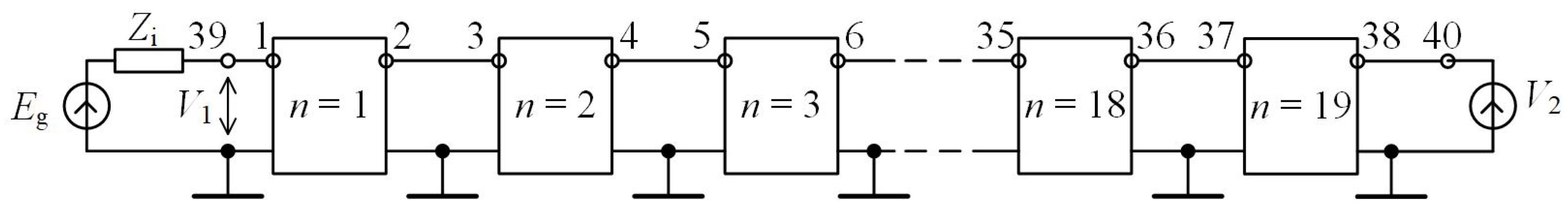
The model is based on a microstrip multiconductor line (MCL), whose structure corresponds to the studied meander structure and is represented as a multiport device (
Figure 1), described by a matrix, Equations (
1) and (
2):
or
where
is a
square scattering matrix of the MCL (in our case,
);
and
are
column matrices describing the incident and reflected scattering parameters.
To find the matrix
, the
A,
B,
C, and
D parameters of the MCL conductors for the even and odd modes are determined with (
3):
where
and where
f is the oscillation frequency;
is the speed of light in a vacuum.
Impedances
and effective dielectric constants
of line conductors are determined by the method of moments [
42]. The calculated values of these parameters for our case are presented in
Table 1.
is the characteristic impedance of the i-th conductor with an even excitation of the line, is the characteristic impedance of the i-th conductor with an even excitation of the line when the dielectric substrate is replaced by a vacuum, is the characteristic impedance of the i-th conductor with an odd excitation of the line, is the characteristic impedance of the i-th conductor with an odd excitation of the line when the dielectric substrate is replaced by a vacuum, is the relative effective permittivity of the i-th conductor with an even excitation of the line, and is the relative effective permittivity of the i-th conductor with an odd excitation of the line.
MCL scattering parameters for even and odd excitation are determined by these (
5) formulas:
While knowing these parameters, it is possible to make a matrix S of the entire MCL.
Since only even and odd excitation of the MCL is considered, only the mutual influence of neighboring conductors is taken into account, and the matrix
S turns out to be sparse (
6)–(
9):
where
Further, the ends of the conductors of the MCL are connected to each other (
Figure 2) so that the required meander structure is obtained and its
parameters are found by the matrix method.
While knowing
parameters, it is possible to find required characteristics and parameters of the system—input and characteristic impedances (
10):
and the transfer function
K of the MS1 structure (
11):
where
is the electromotive force of the signal generator,
is its internal impedance, and
is the load impedance.
The transfer function K is a complex value, its modulus determines the amplitude frequency response, and the argument is the phase frequency response from which the phase delay time of the meander structure can be calculated.
2.2. Computer-Based Models of the Multilayer Meander Structure
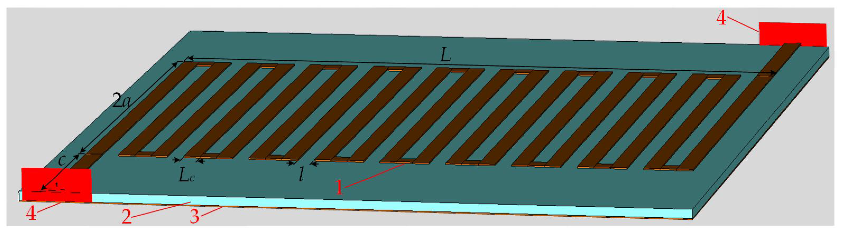
The general mathematical model of the proposed initial meander structure 1 (MS1) is presented in the previous subsection. The MS1 structure is designed in the CST Microwave Studio
© software environment (
Figure 3). The conductor of the meander is positioned in one layer in this particular case. In general, the meander structure consists of a meander-shaped conductor, a dielectric substrate, and a ground shield.
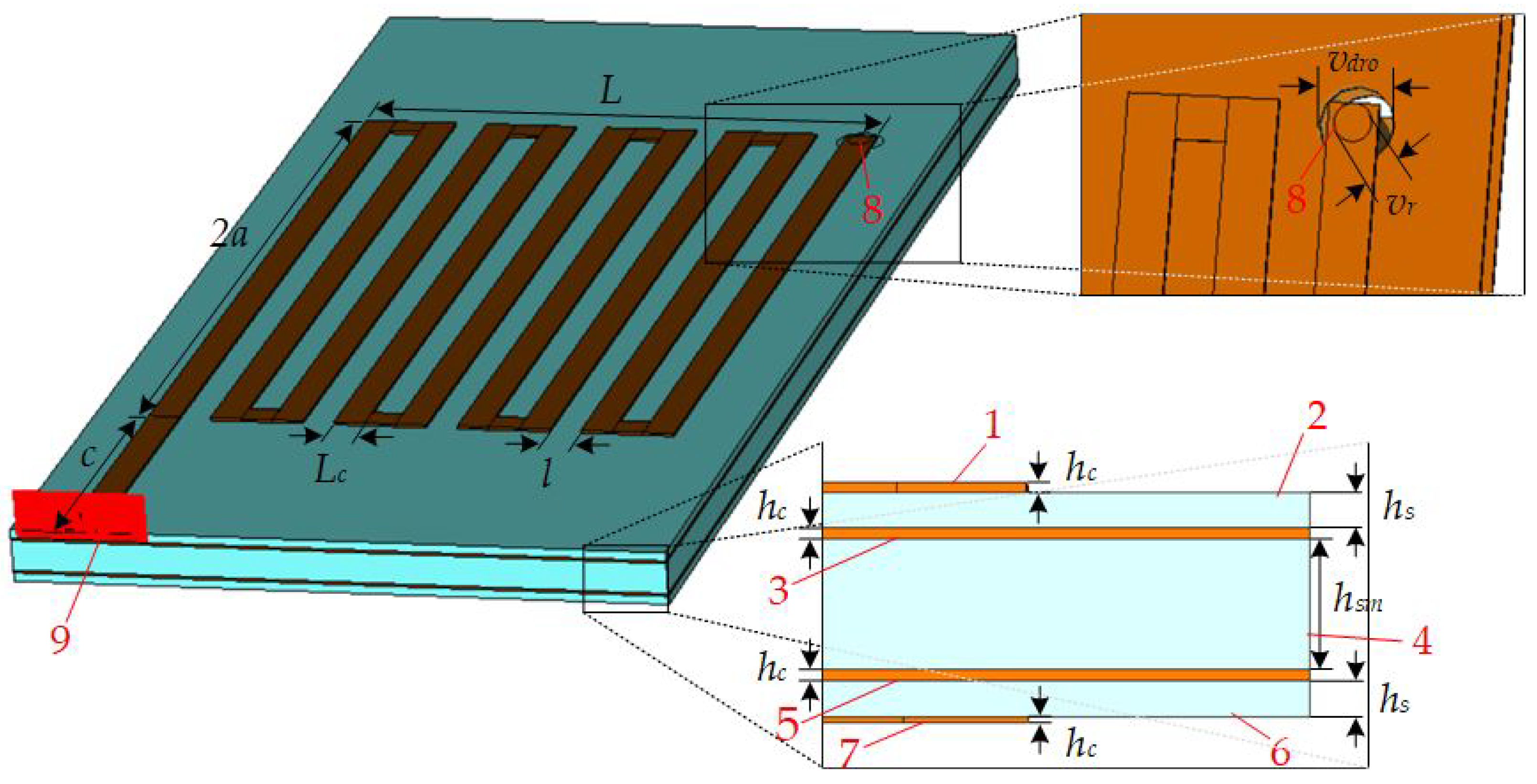
The main dimensions of the presented meander conductor are the following: the overall length of the meander conductor, L = 14.8 mm; the width of the central part of the meander structure, = 10 mm; the length of the additional conductors, c = 3.675 mm; the width of the meander strips, = 0.4 mm; the gap between adjacent conductors, l = 0.4 mm; the thickness of the substrate, = 0.221 mm; the thickness of the conductors, = 0.035 mm. An FR4 material is used for the substrate, where = 4.3 and tan = 0.02. Copper is used for the conductor, whose conductance is equal to S/m. The overall dimensions of the meander structure are mm.
The major focus is concentrated on the miniaturization in this article. Miniaturization is one of the current topics in the manufacturing of modern IoT devices [
43]. The main idea is to maintain the desired performance parameters of the device while miniaturizing the device. The miniaturization task is solved by placing the meander conductor through several PCB layers in this particular article.
First of all, the initial meander structure MS1 (
Figure 3) is miniaturized by breaking the meander structure in half and closing the ground shields of both divided parts of meander structure as a sandwich (
Figure 4). The structure, which is presented in
Figure 4 (left side) will be called meander structure 2 (MS2). The presented construction consists of a top meander conductor, top dielectric substrate, ground shield for both sides of conductors in the middle, bottom dielectric substrate, and bottom meander conductor (
Figure 4, bottom-right corner). The meander conductors, which are positioned in two separated layers, are connected with a connecting via (
Figure 4, top-right corner). A hole with twice the radius of the connecting via is made in the ground shield in order to avoid the interaction between the connecting via and the ground shield.
In practice, the stable and reliable attachment of two separated PCBs of meander structures is obtained by using the plastic screws as it was described in the previously discussed articles. Plastic screws are not presented in the computer model of MS2. The length of the meander conductor on every side of MS2 is reduced by till 7.6 mm. Therefore, the overall dimensions of the designed MS2 structure are mm. On the upper layer of the structure, there is a meander conductor consisting of 10 strips, and on the lower layer, there is a meander conductor of 9 strips (i.e., the total number of strips of both meanders is 19, which corresponds to the initial meander structure of MS1). The length of the overall meander structure is reduced by 7.24 mm, which is a decrease. The thickness of the MS2 structure increased by 0.256 mm till 0.547 mm.
The PCB design of the separated parts of the meander structure is elementary. On the other hand, the disadvantage of MS2 is that it is necessary to have the specific equipment in order to qualitatively attach both parts by plastic screws and qualitatively solder the connecting via. This type of connection is often used in the amateur or small-scale production because it has sufficient rigidity. On the other hand, it is more complicated to use this type of structure in production when a massive manufacture should be performed. By having everything in one PCB, a higher degree of integration will make the overall manufacturing process cheaper in high-quantity production. Most of the time, the PCB costs represent only a small part of the total cost of the device in the massive production.
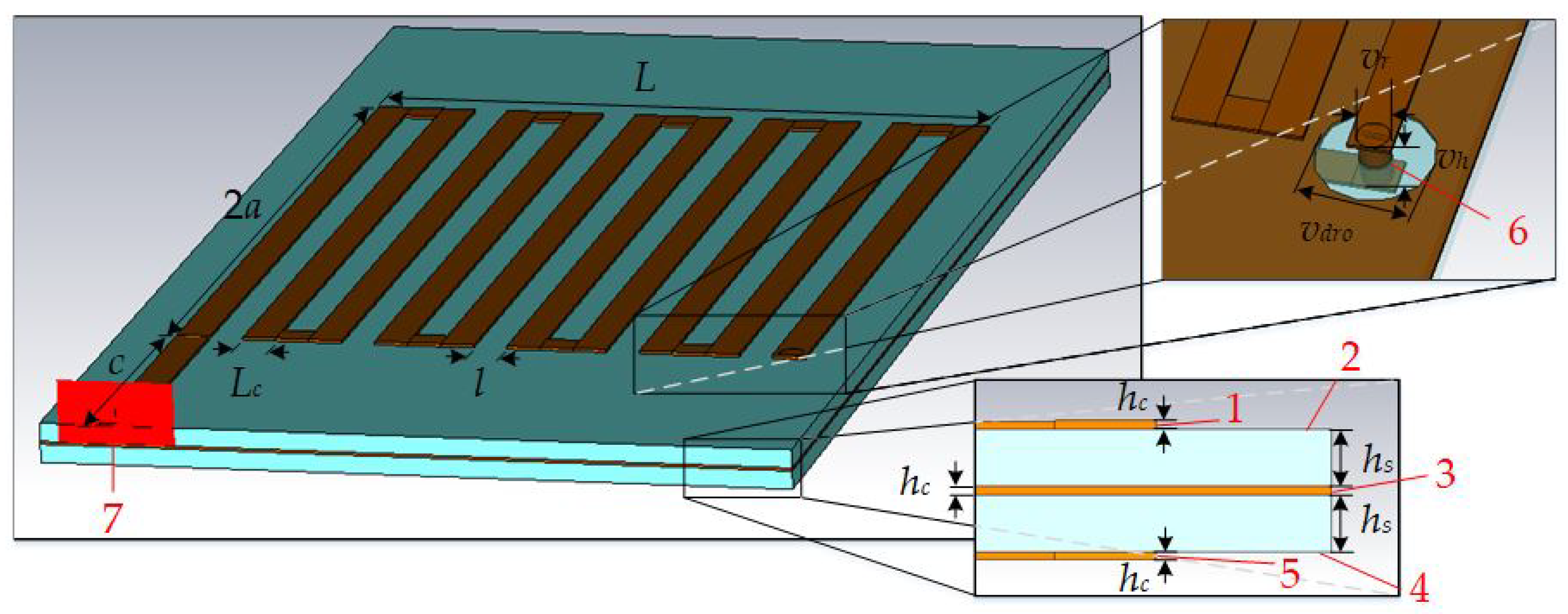
Therefore, a more complicated multilayer construction of the meander structure is designed, which will be titled meander structure 3 (MS3). The presented meander structure MS3 is adapted to the production capacities, which is possible to order from the PCB manufactures. The multilayer meander structure MS3 is presented in
Figure 5 (left side).
The exact height of each MS3 layer is equal to top meander conductor—0.035 mm, top dielectric—0.11 mm, top ground shield—0.035 mm, middle dielectric—0.4 mm, bottom ground shield—0.035 mm, bottom dielectric—0.11 mm, and bottom meander conductor—0.035 mm (
Figure 5, bottom-right corner). The overall dimensions of the designed multilayer meander structure MS3 with the same number of meander strips as MS1 (19 strips) would be equal to
mm. However, further studies have shown that a smaller number of the 17 meander strips is sufficient for this MS3 meander structure. Therefore, 9 strips of the meander are positioned on the top layer, and 8 central conductors of the meander are positioned on the opposite bottom layer (
Figure 5). The overall dimensions of the designed multilayer meander structure MS3 with 17 meander strips are equal to
mm. Only the conductor layers are presented in
Figure 5 (top-right corner). The connection via is isolated from both ground shields by making holes with twice the radius of the connecting via in both ground shields.
The time-domain solver was utilized in CST Microwave Studio© with the default parameters during the computer-based modeling. A hexahedral (legacy) mesh with a −40 dB accuracy was used for the modeling of the meander structure. CST Microwave Studio© employs methods such as adaptive meshing, which dynamically adjusts the mesh resolution based on the electromagnetic field variations in order to maintain accuracy and stability in simulations. S-parameters were normalized to a fixed impedance. The 0–10 GHz frequency range was investigated with the 0.01 maximum delta parameter and a single check. A total of 50 pulses were applied to the line. For stability considerations, a stability factor of 1 was initially chosen, accompanied by features such as restarting the solver after instability abort, considering a two-port reciprocity with an energy balance limit of 0.03 and employing automatic time signal sampling. An attempt was made to decrease the stability factor to 0.95, but as no significant differences were observed, the stability factor was reverted to a value of 1. The absence of stability criteria warnings or errors during the simulation process indicates stability.
The designed MS3 meander structure was manufactured and is presented in the next subsection of models for the experimental investigation.
2.3. Experimental Models of the Multilayer Meander Structure
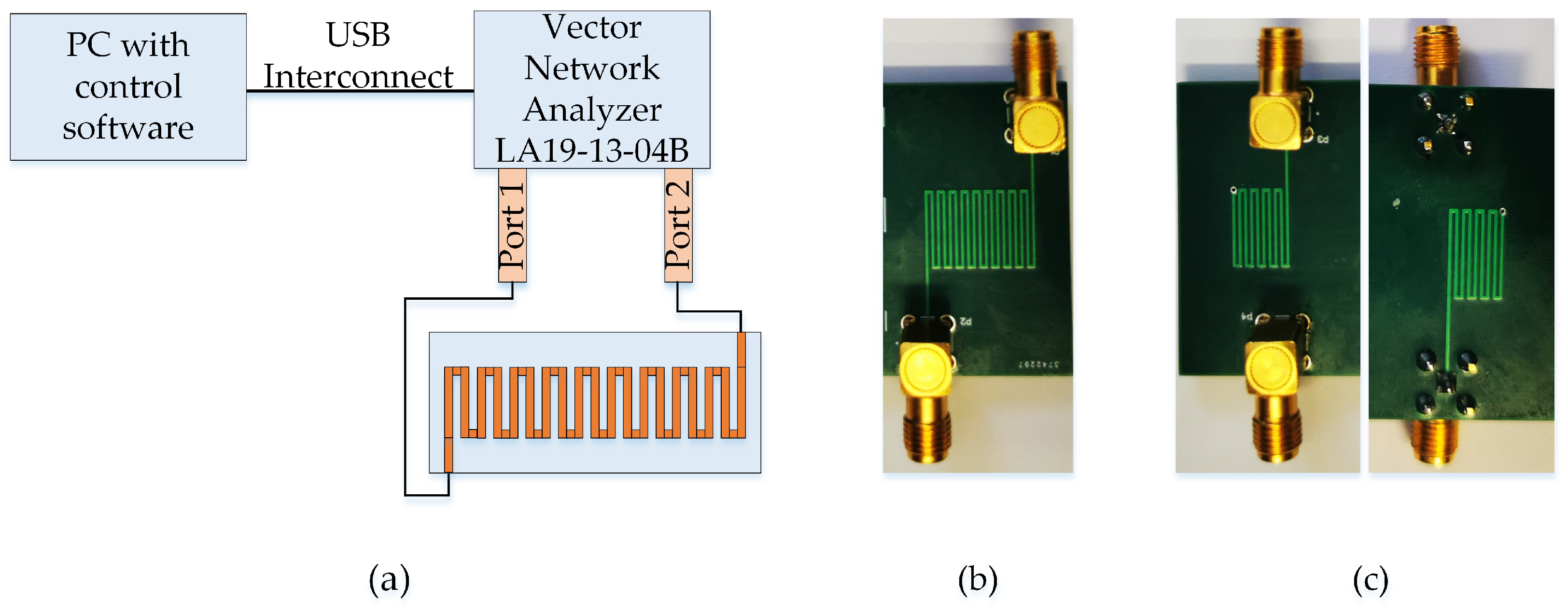
The PCBs of the one-layer MS1 and the multilayer meander structure MS3 were designed using the Altium Designer© (Altium Designer 2010, Altium, La Jolla, CA, USA, 2010) software package. The PCB of the multilayer meander structure was designed with the same design parameters as in the computer-based simulation.
Different variants of the multilayer meander structures are manufactured for testing. The top view of the initial meander structure MS1 is presented in
Figure 6b. The initial meander structure MS1 has 19 meander strips. The top and bottom views of the multilayer meander structure MS3 are presented
Figure 6c. The presented MS3 model is with 19 meander strips (10 strips in the top layer and 9 strips in the bottom layer). The position of the connecting via could be seen in top and bottom views of MS3. Later, the additional MS3 model of the meander structure with 17 meander strips was manufactured in order to produce a structure as similar as possible to the initial MS1 in its passband and delay time.
The overall dimensions and all other parameters are the same as during the computer-based modeling. The dimensions of the manufactured MS3 structure are as follows: L = 6.8 mm, = 10 mm, c = 3.675 mm, = 0.4 mm, l = 0.4 mm, = 0.11 mm, = 0.4 mm, = 0.035 mm, = 0.15 mm, = 0.547 mm, = 0.15 mm, and = 0.55 mm. The substrate is manufactured using the FR4 Kingboard tg150 material, where = 4.3 and tan = 0.02. Conductive layers were made from copper, the conductivity of which is S/m. The overall dimensions of the manufactured MS1 are equal to mm. The overall dimensions of MS3 with 19 central conductors are equal to mm. SMA connectors were used for the connection.
The
S reflection and
S transmission parameters were measured using the LA19-13-04B vector network analyzer (VNA). A block diagram with the equipment of the experimental measurement is presented in
Figure 6a. The LA19-13-04B VNA is connected to the PC using the USB interface. The LA19-13-04B vector analyzer has an 8.5 GHz frequency range and is capable of measuring the required S parameters. Two SMA connectors were soldered on both ends of every meander structure. The input of the meander structure through the SMA connector was directly connected to the VNA, whereas the second end was connected to the second port of the VNA using a low-loss Sucoflex 126EA cable. The calibration phase and obtaining of the results were performed using the recommendations of the manufacturer. The most common short-open-load-thru (SOLT) calibration method was used. SOLT requires a short circuit, an open circuit, a load of the same values as the system impedance and through line configurations. The reference plane was on the VNA connector after the calibration. The mechanical commercial calibration kit was provided by the manufacturer. The
t characteristics were calculated from the measured
S phase characteristics.
3. Results
MS1, MS2, and MS3 meander structures are investigated using analytical calculations, computer-based simulations, and physical experiments. Results of the investigation are presented in
Figure 7,
Figure 8,
Figure 9,
Figure 10,
Figure 11,
Figure 12,
Figure 13,
Figure 14,
Figure 15,
Figure 16,
Figure 17,
Figure 18 and
Figure 19.
3.1. Computer-Based Simulation Results
Frequency dependences of coefficient
and delay time
were calculated using the computer-based simulations of the meander structures with the CST Microwave Studio
© software package and are presented in
Figure 7,
Figure 8,
Figure 9,
Figure 10,
Figure 11 and
Figure 12.
First of all, a comparison of frequency dependences of
and
of the meander structure with the different number of layers is presented in
Figure 7 and
Figure 8. A comparison of
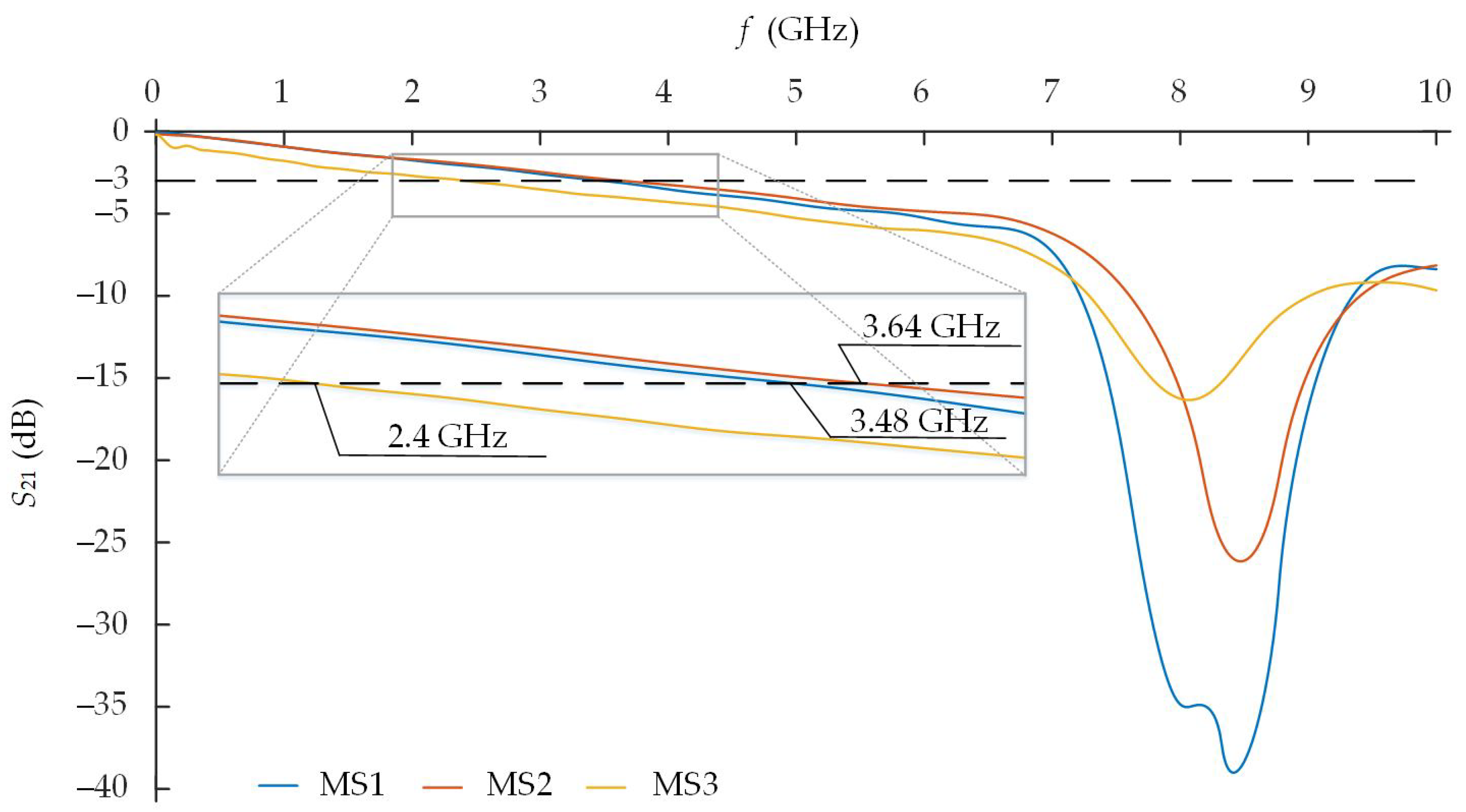
characteristics of three different MS1, MS2, and MS3 structures is presented in
Figure 7. The overall length of the meander conductor is the same in all three cases. All three models of meander structures have 19 meander strips. The blue line represents the initial MS1 model of the meander structure when the structure consists of conductor–dielectric–ground shield layers (
Figure 3). The red line represents the MS2 model of the meander structure, which consists of the conductor–dielectric–ground shield–dielectric–conductor layers (
Figure 4). The yellow line represents the MS3 model of the meander structure, which consists of conductor–dielectric–ground shield–dielectric–ground shield–dielectric–conductor layers (
Figure 5). Design parameters of the meander structures with a different number of layers are presented in the section of materials and methods.
Figure 7.
Frequency dependences of of the MS1, MS2, and MS3 meander structures with a different number of layers when the number of strips is equal to 19.
Figure 7.
Frequency dependences of of the MS1, MS2, and MS3 meander structures with a different number of layers when the number of strips is equal to 19.
Frequency dependences of
and
of the MS1, MS2, and MS3 meander structures that are presented in
Figure 7 and
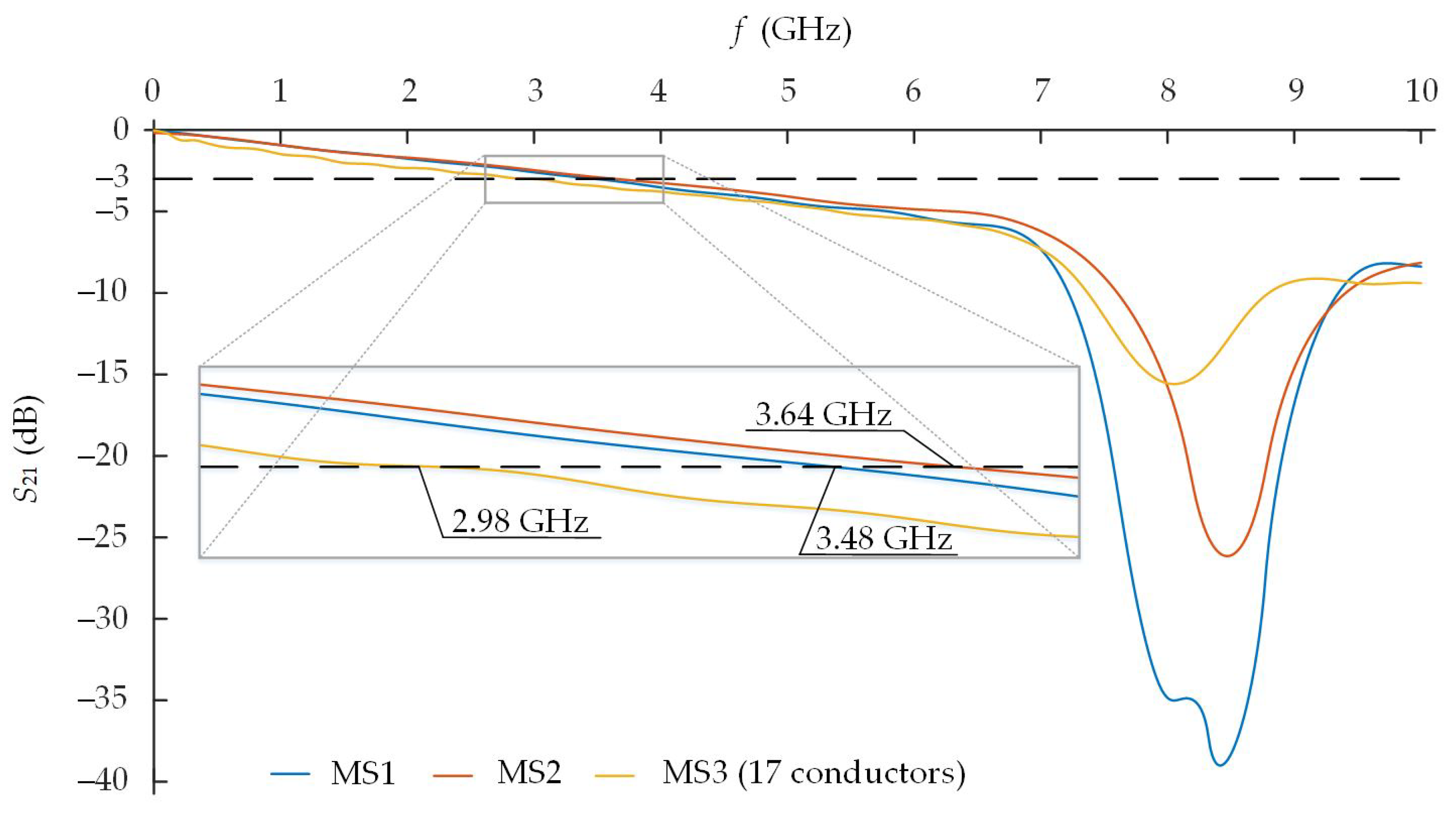
Figure 8, respectively, have shown that the different number of layers has an impact on the passband of the meander structure. The passband of the MS1 meander structure is equal to 3.64 GHz. The cutoff frequency of the MS2 meander structure has decreased by 160 MHz till 3.48 GHz when the meander conductor was positioned in two separated layers. The cutoff frequency of the MS3 meander structure decreased by 1.24 GHz till 2.4 GHz when it was adjusted to the production possibilities (
Figure 7).
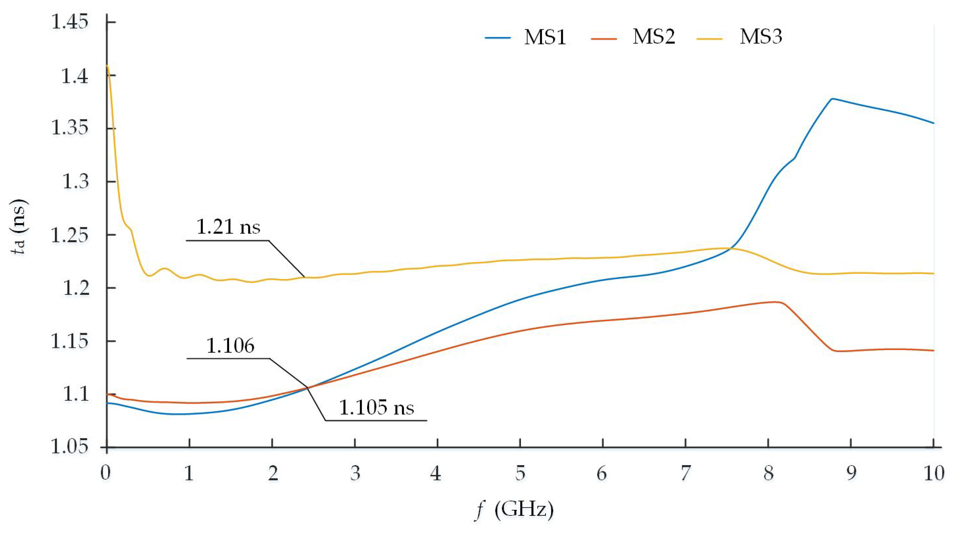
Frequency dependences of
(
Figure 8) have shown that the number of layers as well as the length of the transitions themselves between the layers has an impact on the
of the meander structure. The
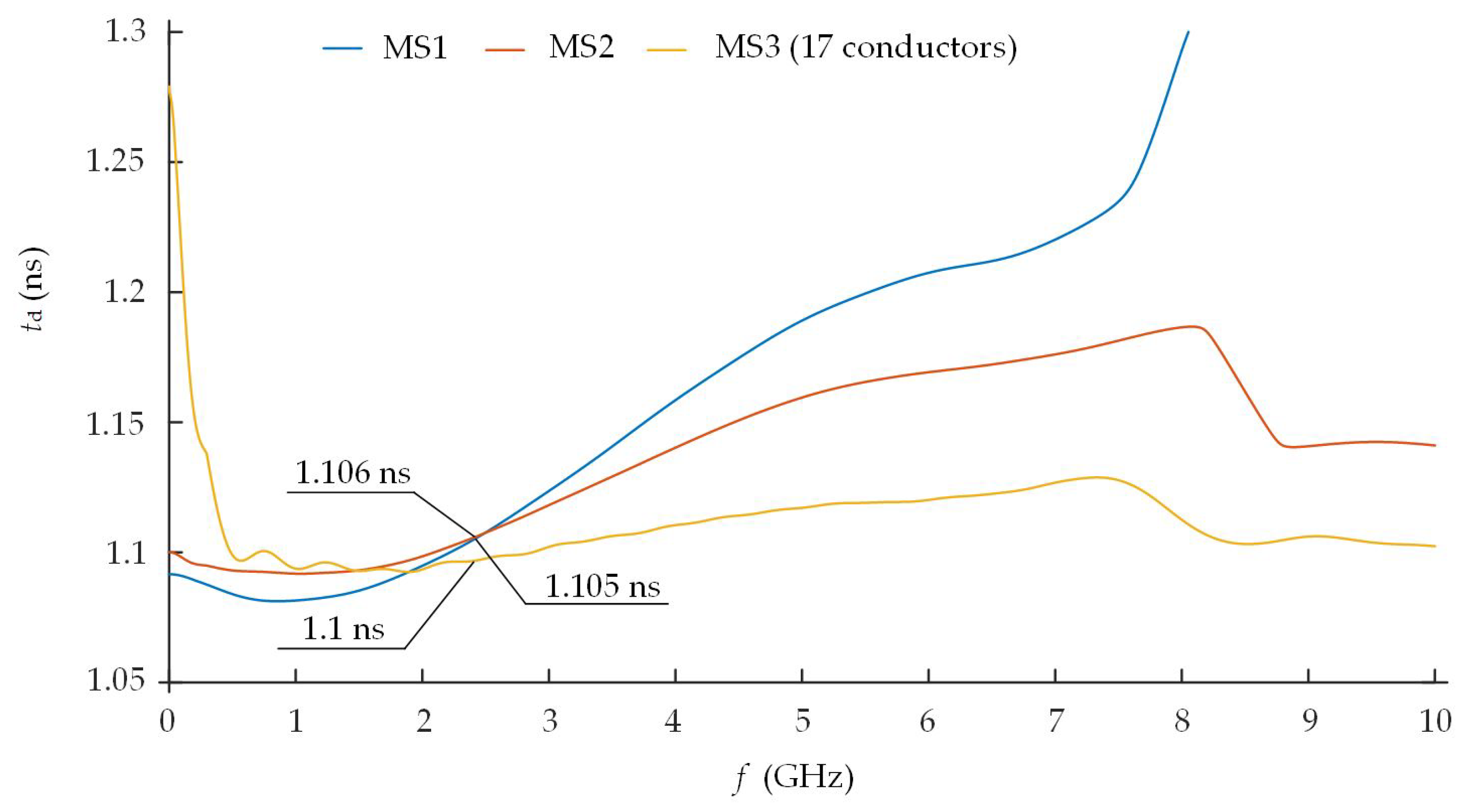
of the MS2 meander structure is of similar level compared with the MS1 model. The delay times of both models are practically equal at a frequency range of 2.4–2.5 GHz. The
of the MS1 structure is equal to 1.105 ns at a 2.4 GHz frequency. The
of the MS2 structure is equal to 1.106 ns. MS2 has a bit faster growth of
at higher frequencies. Meanwhile, the MS3 model has a 0.1 ns higher level of the delay time that is equal to 1.21 ns and is almost constant across the overall passband except the low frequencies. Larger fluctuations can be influenced by the unevenness of the characteristic impedance that is caused by the connecting via.
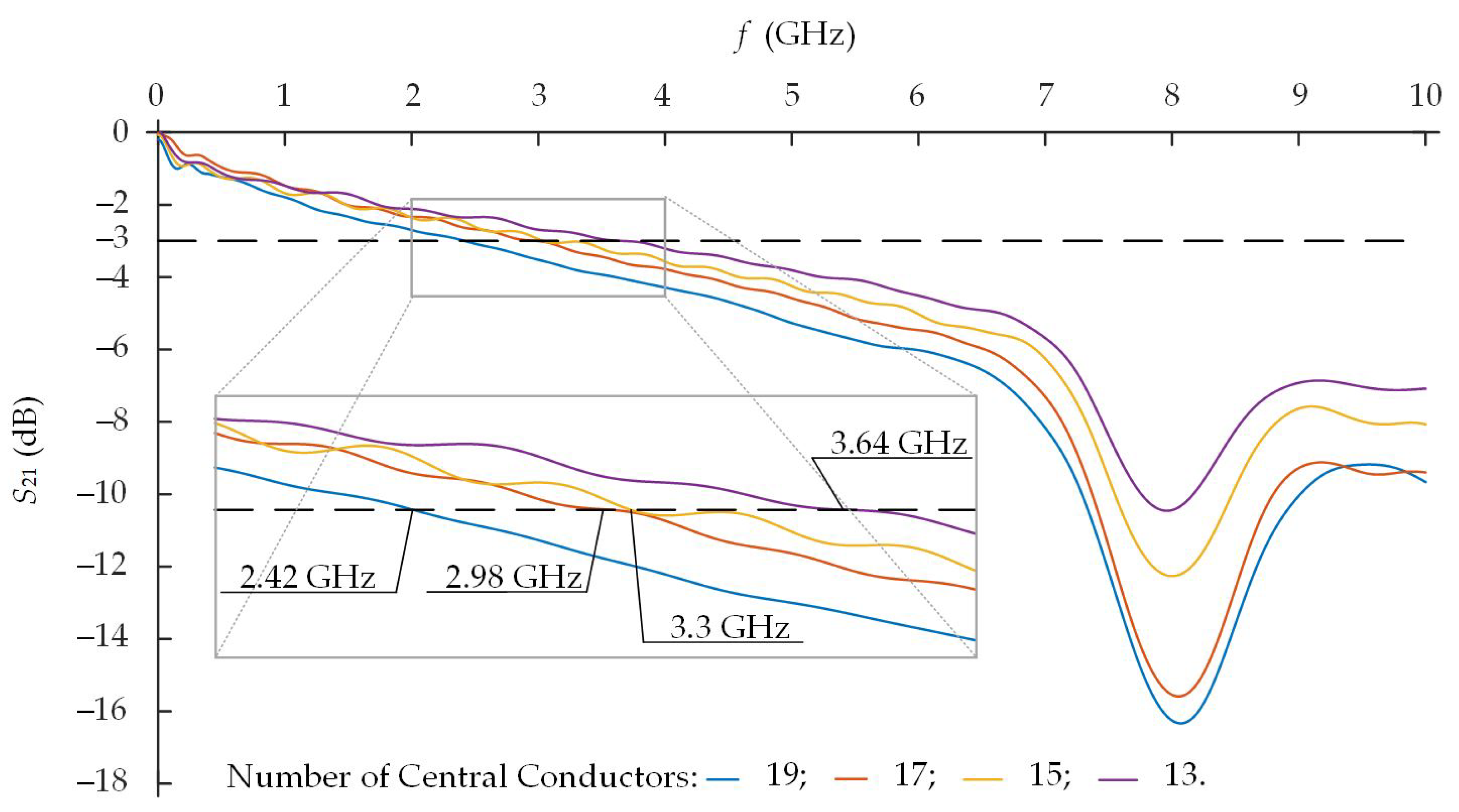
Simulated frequency dependences of
and
of the MS3 model of the meander structure with the different number of strips (13, 15, 17, and 19 strips, respectively) are presented in
Figure 9 and
Figure 10.
The positive feature of an MS3 meander structure is the miniaturized dimensions and bigger
. On the other hand, because of the bigger number of layers, a thinner dielectric layer between the meander conductor and the grounded shield and due to the longer connecting via, the MS3 model has a narrower passband. The variation of the number of meander strips allows for controlling the cutoff frequency of the passband. The decrease of the number of meander strips from 19 till 13 allowed for a wider passband from 2.42 GHz till 3.64 GHz (
Figure 9). Thus, the decrease of meander strips allowed for increasing the passband and having almost the same passband as the MS1 meander structure.
Figure 8.
Frequency dependences of of the MS1, MS2, and MS3 meander structures with a different number of layers when the number of strips is equal to 19.
Figure 8.
Frequency dependences of of the MS1, MS2, and MS3 meander structures with a different number of layers when the number of strips is equal to 19.
Figure 9.
Frequency dependences of of the MS3 meander structure when the number of strips is equal to 13, 15, 17, and 19.
Figure 9.
Frequency dependences of of the MS3 meander structure when the number of strips is equal to 13, 15, 17, and 19.
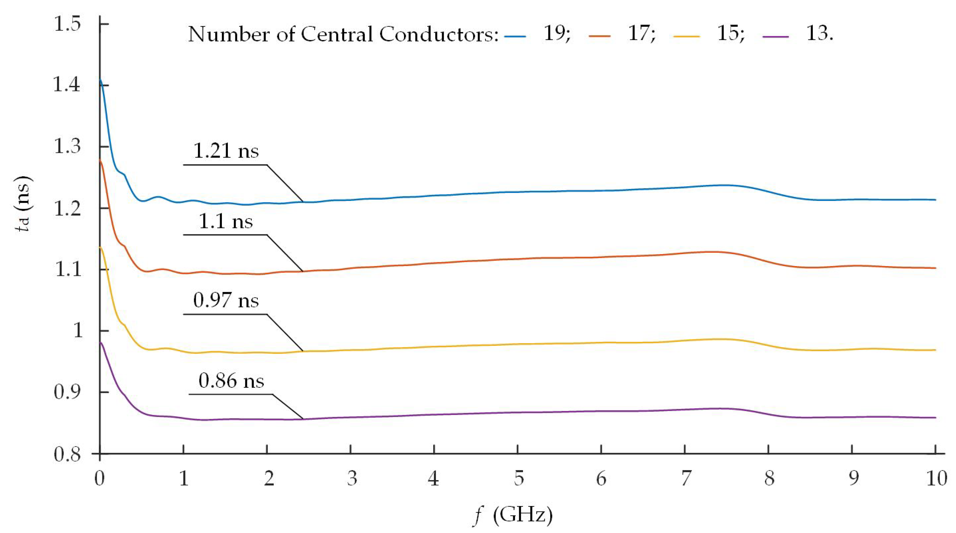
On the other hand, the decrease of the number of meander strips from 19 till 13 has a significant impact on the
of the MS3 model (
Figure 10). The
decreased from 1.21 ns till 0.86 ns.
The number of strips of MS3 was decreased from 19 till 17 in order to design the multilayer meander structure MS3 that operates as close as possible (equal
and the cutoff frequency higher than 2.4 GHz) to the initial meander structure MS1. For comparison, the frequency dependencies of
and
of the meander structures MS1, MS2 (19 strips each), and MS3 (17 strips) are shown in
Figure 11 and
Figure 12.
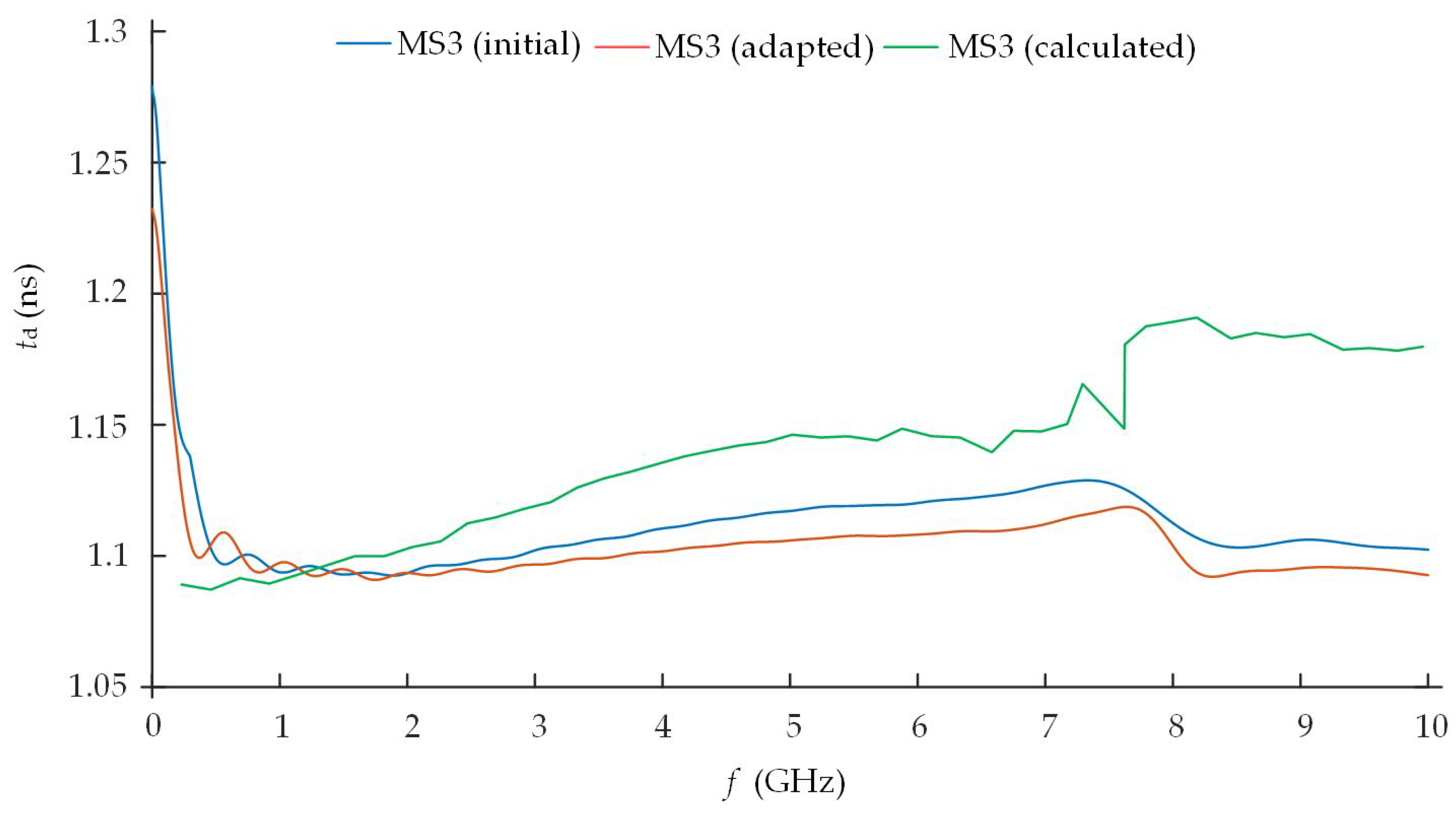
The value of frequency dependences of the delay time
characteristic of the MS3 model with 17 strips is equal approximately to 1.1 ns and is stable in the operating 2.4–2.5 GHz ISM frequency range (
Figure 11). The delay time of MS1 is equal to 1.106 ns. The delay time of MS2 is equal to 1.105 ns at the 2.4 GHz frequency. The differences in comparison between all three models do not exceed 6 and 5 ps, respectively (0.55% and 0.45%, respectively).
Figure 10.
Frequency dependences of of the MS3 meander structure when the number of strips is equal to 13, 15, 17, and 19.
Figure 10.
Frequency dependences of of the MS3 meander structure when the number of strips is equal to 13, 15, 17, and 19.
Figure 11.
Frequency dependences of of the meander structures MS1, MS2 (19 strips each), and MS3 (17 strips).
Figure 11.
Frequency dependences of of the meander structures MS1, MS2 (19 strips each), and MS3 (17 strips).
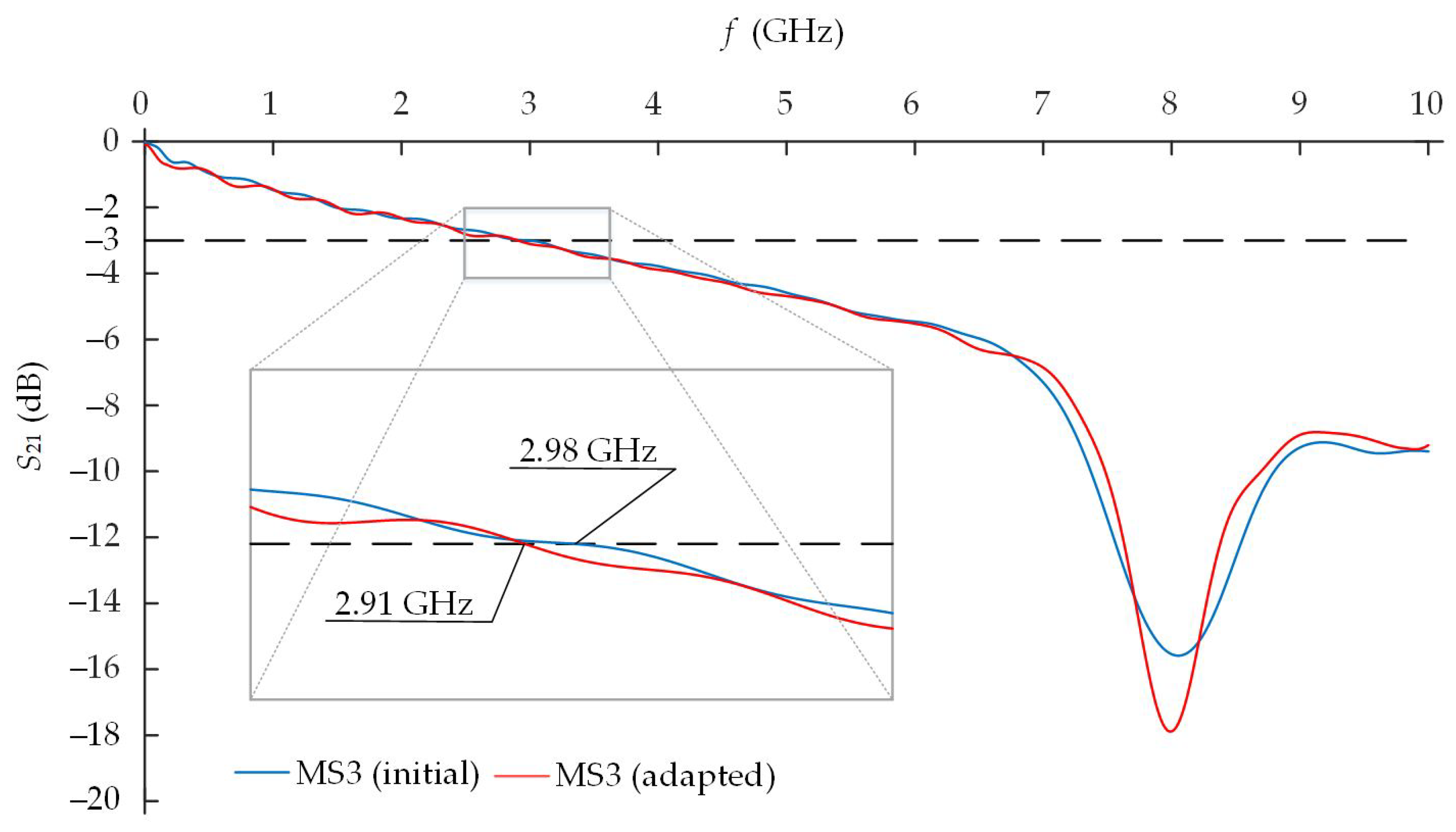
The passband of such MS3 model with 17 strips is till 2.98 GHz (
Figure 12). Therefore, it is capable of working in the 2.4–2.5 GHz ISM frequency range.
In summary, the designed MS3 meander structure allowed for maintaining almost the same while miniaturizing the length of the entire meander structure by 48% from 16.24 mm till 8.40 mm in comparison with the MS1 structure, while the thickness of the meander structure increased by 0.469 mm. On the other hand, the cutoff frequency of the passband decreased from 3.64 GHz till 2.98 GHz (−18%). However, MS3 is still appropriate for the IoT devices working in the 2.4–2.5 GHz ISM frequency range.
A sharp decrease in
values and an increase in
at frequencies of 7–9 GHz are explained by resonant phenomena, when the half-wave length of the
waveguide corresponds to the length of the meander strips (in our case, 10 mm).
Figure 12.
Frequency dependences of of the meander structures MS1, MS2 (19 strips each), and MS3 (17 strips).
Figure 12.
Frequency dependences of of the meander structures MS1, MS2 (19 strips each), and MS3 (17 strips).
3.2. Results of Experimental Investigation
Results of the computer-based simulations with CST Microwave Studio
© are verified with a physical experiment and also calculations with an analytical
matrix method. Measurements were made using the LA19-13-04B vector network analyzer. Two separated cases are presented for a comparison. These cases summarize and perfectly reflect all the other cases during the investigation. A comparison of results with all three methods are presented in
Figure 13 and
Figure 14.
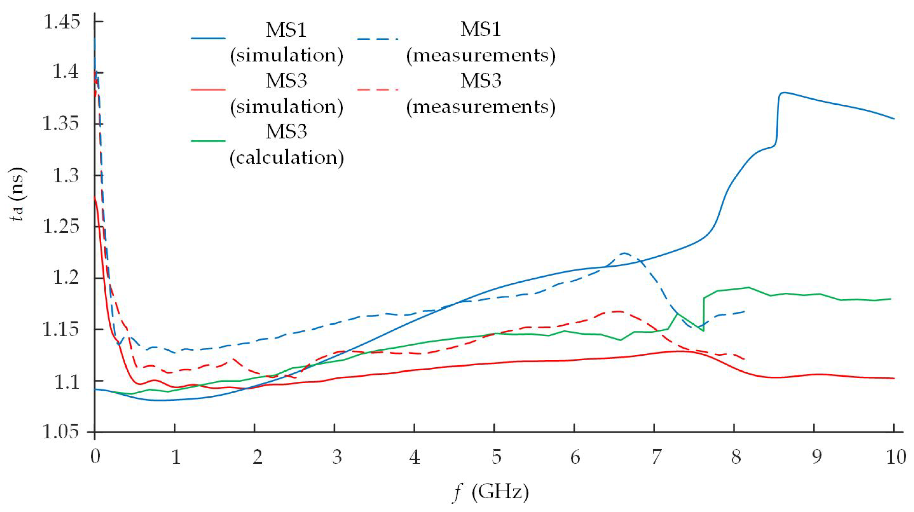
The comparison of the measured and simulated frequency dependences of
showed that the difference of the delay time between simulated and measured
of the meander structure MS1 is equal to 35 ps (3.2%) at 2.4 GHz. The difference of simulated, calculated, and measured
of the MS3 model of the meander structure does not exceed 5 ps (0.5%) at 2.4 GHz (
Figure 13). It should be emphasized that the comparison of
also includes calculations using the analytical
matrix method (
Figure 13, green solid curve), which is discussed in detail in the materials and methods section. The results of MS3 well correlated with all three methods in the ISM frequency band.
Figure 13.
Simulated, calculated, and measured frequency dependences of characteristics of the MS1 (19 strips) and MS3 (17 strips) meander structures.
Figure 13.
Simulated, calculated, and measured frequency dependences of characteristics of the MS1 (19 strips) and MS3 (17 strips) meander structures.
It should also be emphasized that the results of the computer-based simulation and analytical calculations are presented up to 10 GHz. Meanwhile, the results of measurements are presented up to 8.192 GHz, as these are the limits of the used LA19-13-04B VNA.
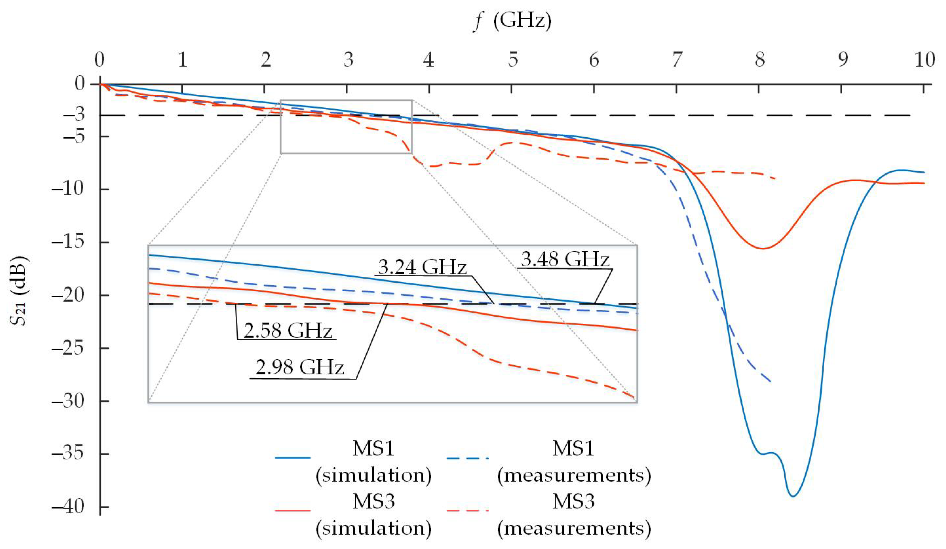
Measured and simulated frequency dependences of
are presented in
Figure 14. The difference between the simulated and measured cutoff frequencies of the meander structure MS1 is equal to 240 MHz (6.8%). The cutoff frequency of the simulated MS1 is equal to 3.48 GHz. The cutoff frequency of the measured MS1 is equal to 3.24 GHz. The cutoff frequency that was obtained from the physical experiment of the MS3 model is equal to 2.58 GHz, while the simulated value of MS3 is equal to 2.98 GHz. The discrepancy between the simulated and measured values of MS3 is equal to 400 MHz (13.4%). On the other hand, the meander structure is still capable of working in the 2.4–2.5 GHz ISM frequency band.
Figure 14.
Simulated and measured frequency dependences of the characteristics of the MS1 (19 strips) and MS3 (17 strips) meander structures.
Figure 14.
Simulated and measured frequency dependences of the characteristics of the MS1 (19 strips) and MS3 (17 strips) meander structures.
It could be noticed that without differences in passband, there are also some discrepancies that almost reach 3 dB between measured and simulated frequency dependences of
in the stop band, especially in the range of 3.5–5 GHz (
Figure 14). These differences occurred only in the multilayer MS3 structure. There could be various reasons for these differences. First of all, there will be a jump of characteristic impedance in this range of frequencies. The increase in characteristic impedance should be caused by the inductive elements in the meander line. The meander structure can be effectively represented by a two-port circuit model, where each section of the structure is replaced with an equivalent circuit comprising inductive and capacitive elements. In the case of such reasons, such a difference between simulated and measured characteristics is possible and likely, since approximation is used in the computer-based simulation, which eliminates this type of fluctuations. Meanwhile, the measured results were not approximated.
Moreover, the reference plane was selected on the VNA connector during calibration. This means that the SMA connectors influence the results of measurements. The SMA connectors were not designed during the simulation. Therefore, the effect of the coaxial to microstrip transition should not be visible. On the other hand, the port de-embedding was used during the simulation with a time-domain solver. The impedance was normalized to the fixed value.
It is possible to shift the measurement reference plane away from the value set during calibration, which can be useful in removing the effect of interconnecting cables or microstrip lines from measurements. However, we chose to keep the same reference plane for all variations. Our future works include the more accurate analysis of the simulation methods in order to take into account previously mentioned factors.
Variation of the parameters
and tan
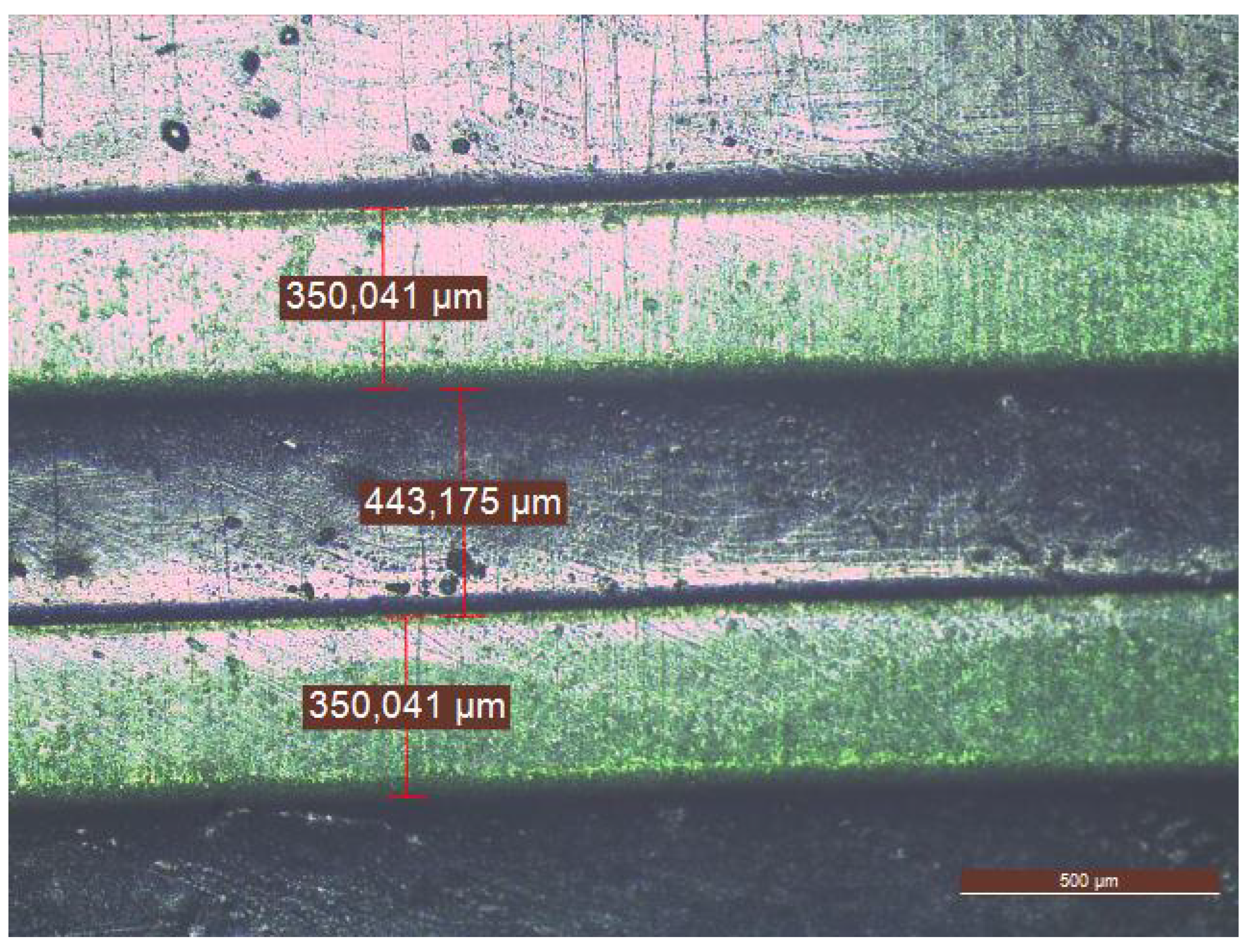
of the materials used, as well as manufacturing errors, could also have a noticeable impact on the performance of microwave devices. Manufacturing inaccuracies is a widely analyzed topic and is discussed in the introduction section. The manufacturing error of the width of the meander strips and gaps between them was investigated with a Leica DM750M binocular materials microscope that allows for a full range of magnifications between 50× and 1000×. The typical results of the meander PCB from the top are presented in
Figure 15, when the width of the meander strip
mm and the gap between the meander strips was
mm. Only the width of the strips and gaps between them was investigated from the top. The cross-sectional manufacturing errors were not investigated, which could also have a huge impact on the manufacturing error.
Figure 15.
The zoomed fragment of the top view of the MS3 meander structure with the measured width of the meander strips and gap between the strips using a Leica DM750M binocular materials microscope.
Figure 15.
The zoomed fragment of the top view of the MS3 meander structure with the measured width of the meander strips and gap between the strips using a Leica DM750M binocular materials microscope.
The PCB manufacturer provides the information that the maximum manufacturing error is ±0.0381 mm for line widths greater than 0.254 mm. We made the measurements with a Leica DM750M microscope in order to check the actual manufacturing error of the widths of the meander strips and gaps between the meander strips. It is seen that the manufacturing error of the strip’s width typically does not exceed and is wider by 0.041 μm (0.1%). The gap between the meander strips is typically wider by 44 μm (1.25%) (
Figure 15).
In order to check the influence of the observed manufacturing errors, first of all, the additional simulation was made with CST Microwave Studio
©. The results of the simulation are presented in
Figure 16 and
Figure 17.
The results of
showed that the influence of a manufacturing error practically do not impact the
characteristic at the ISM frequency band. The comparison of the initial MS3 structure with 17 meander strips and the adopted MS3 structure according to the measurements with a Leica DM750M microscope showed that the difference was only 2 ps at 2.4–2.5 GHz (0.2%) (
Figure 16). The calculated frequency dependences of the
characteristic using the analytical
matrix method is also provided in
Figure 16 for a comparison. The difference between the simulated and calculated frequency dependences of
does not exceed 16 ps (1.5%) in the ISM frequency band.
Figure 16.
Simulated and calculated frequency dependences of of the initial and adapted-to manufacturing error MS3 structure (17 strips).
Figure 16.
Simulated and calculated frequency dependences of of the initial and adapted-to manufacturing error MS3 structure (17 strips).
The results of the simulation of the frequency dependences of the
characteristics of the initial and adapted-to manufacture error MS3 showed that the manufacturing error shifted the cutoff frequency of the MS3 structure by 70 MHz from 2.98 GHz till 2.91 GHz (
Figure 17). Thus, the difference is insignificant.
Figure 17.
Simulated frequency dependences of of the initial and adapted-to manufacturing error MS3 structure (17 strips).
Figure 17.
Simulated frequency dependences of of the initial and adapted-to manufacturing error MS3 structure (17 strips).
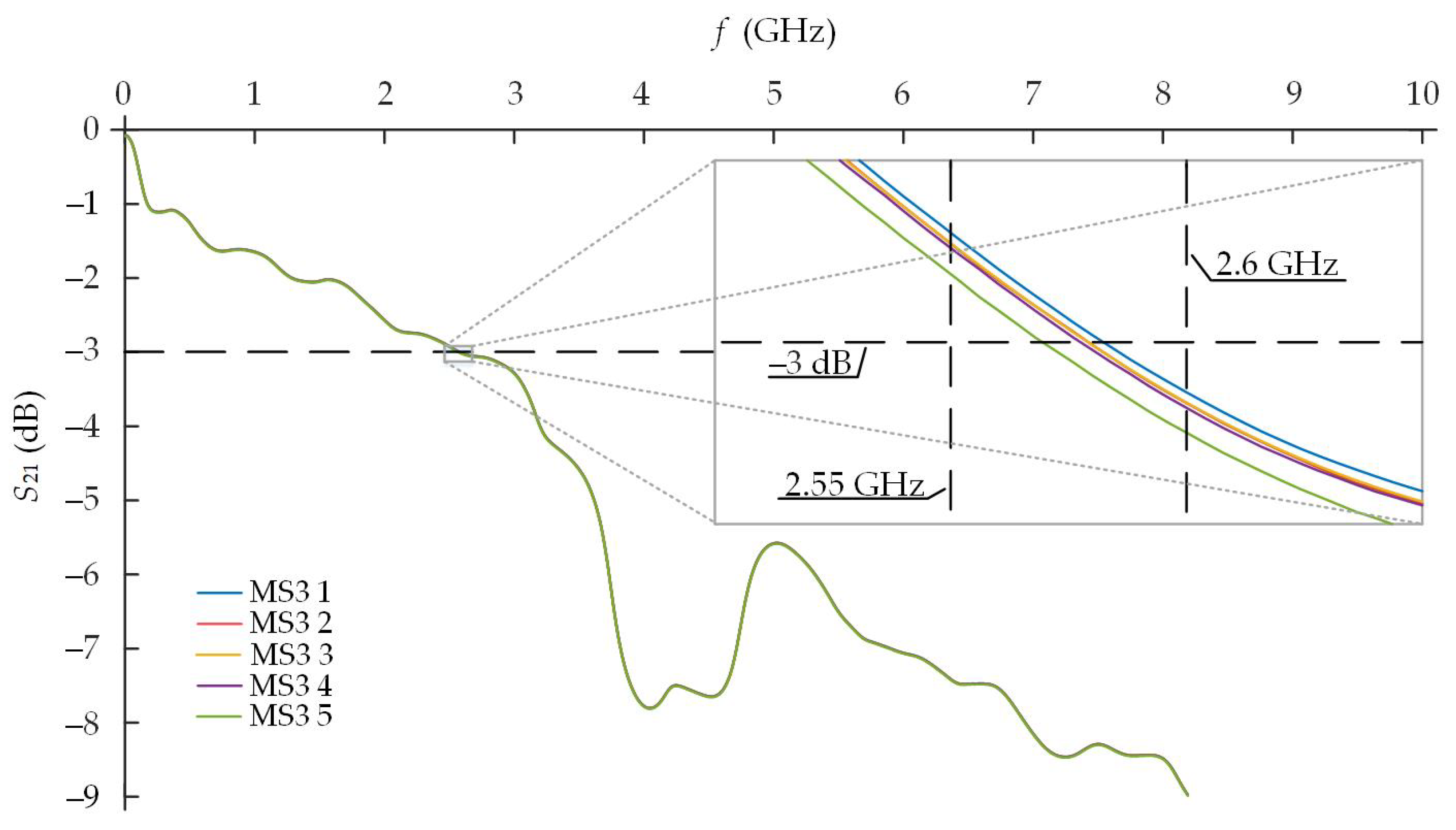
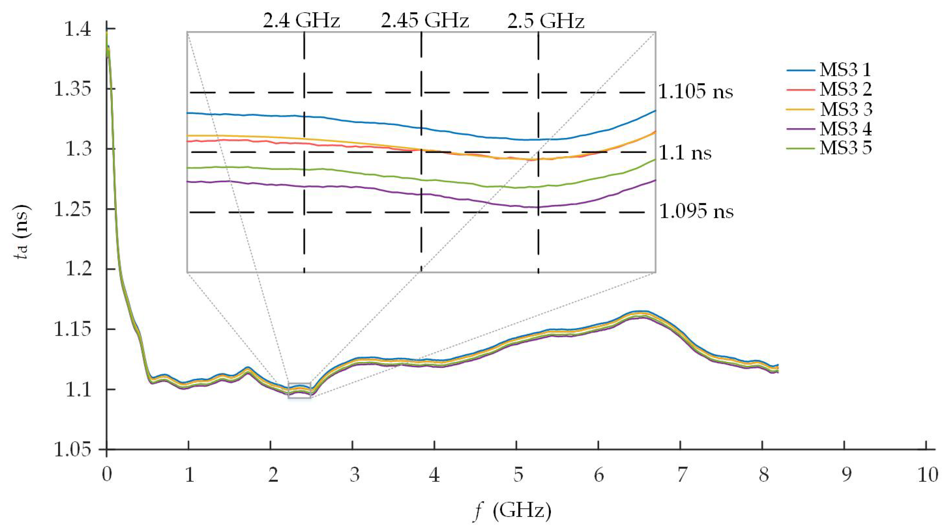
We would also like to emphasize that five units of each prototype of the different meander structure were produced. Measurements with the LA19-13-04B VNA were repeated with each of the five units of the same meander structure. The measured
practically agree (
Figure 18). The variation of the cutoff frequency did not exceed 12 MHz (0.4% of passband). The obtained deference could be influenced not only by the manufacturing error but also with the quality of soldering of the SMA connectors.
Figure 18.
Measured frequency dependences of of every of 5 units of the MS3 (17 strips) meander structures.
Figure 18.
Measured frequency dependences of of every of 5 units of the MS3 (17 strips) meander structures.
The difference of the delay time
did not exceed 10 ps (1%) (
Figure 19).
Figure 19.
Measured frequency dependences of of every 5 units of the MS3 (17 strips) meander structures.
Figure 19.
Measured frequency dependences of of every 5 units of the MS3 (17 strips) meander structures.
In summary, from the previously discussed results, it is seen that the variation dynamics of the simulated and measured characteristics coincide. However, the numerical values of the measured frequency dependences of the phase (group) delay time are slightly higher than the analogous values of the simulated dependences. This may be due to the mismatched characteristic impedance of the simulator ports, vector analyzer, and studied meander structures or not evaluating all factors when modeling meander structures, for example, the effect of the coaxial to microstrip transition. In summary, the area of the connecting via may require additional attention due to impedance discontinuity, followed by the stronger signal reflection.
4. Discussion
Our previous research [
40] showed positive features of the meander structures when the passband, delay time, and input impedance characteristics could be controlled without changing the dimensions of the overall meander structure. In this article, the miniaturization task was solved when the overall size of the meander structure was reduced from
mm till
mm while maintaining the same electrodynamical parameters of the meander structure.
Computer-based simulations, analytical calculations, and measurements results, which were presented in the previous section, showed that it is possible to reduce the overall dimensions of the meander structure by positioning the meander strips in the multiple layers. It was also noticed that the aspiration to decrease the overall dimensions of the meander structure by using several layers of the PCB increases the delay time of the meander structure by the order of ps. In our particular case, the delay time was increased in average from 1.09 ns till 1.21 ns. However, the passband of the meander structure decreased significantly by 1.22 GHz from 3.64 GHz till 2.42 GHz, when the MS1 and MS3 meander structures were compared.
It is also necessary to emphasize that the MS2 meander structure allowed for keeping an almost stable delay time characteristic in the passband area, but the passband defined at −3 dB decreased by 160 MHz from 3.64 GHz till 3.48 GHz in comparison with the MS1 meander structure. It should be noted, however, that the production of such a structure in a large-scale production is very problematic.
The results of the physical experiments verified the results of the computer-based simulation. Frequency dependences from simulation and experimental data have very similar variation dynamics. However, the values of the measured dependences are higher by the same level through all the range of frequencies. This may be due to not evaluating all factors when modeling meandering structures. The difference of did not exceed 5 ps (0.5%) in the ISM frequency band.
A narrower passband when increasing the number of layers is influenced by the irregularities of the characteristic impedance that occur in the connecting via. Other factors of the narrower passband could be the increased number of layers and the thinner dielectric layer between the meander conductor and the grounded shield. A more detailed analysis of the connecting vias was not carried out in this article. This was because it was enough for the designed multilayer MS3 meander structure in order to achieve miniaturization goals while maintaining the same delay time and ensuring correct functioning at a 2.4–2.5 GHz ISM frequency band.
The general mathematical model of the meander structure was also presented. The analytical calculations also verified the results of the computer-based simulation and physical experiment, thus confirming that the mathematical model is suitable and can be applied in further analysis.
Future works will include a more detailed analysis of the connecting and grounding vias in order to decrease the impact of a number of layers on the cutoff frequency of the passband. The elimination of the causes of the unevenness of the characteristic impedance may also lead to new opportunities for reducing the dimensions of the multilayer meander structures.


 ,
, 

