Article

Effect of Non-Ideal Cross-Sectional Shape on the Performance of Nanosheet-Based FETs

1
School of Microelectronics, Xidian University, Xi’an 710071, China
2
Department of Electrical and Computer Engineering, McMaster University, Hamilton, ON L8S 4K1, Canada
*
Author to whom correspondence should be addressed.
Electronics 2023, 12(16), 3419; https://doi.org/10.3390/electronics12163419
Submission received: 27 June 2023 / Revised: 1 August 2023 / Accepted: 2 August 2023 / Published: 11 August 2023
(This article belongs to the Special Issue Advanced CMOS Devices)

Abstract

:
In this article, the effects of non-ideal cross-sectional shapes of stacked nanosheet FET (NSFET) and nanosheet FET with inter-bridge channel (TreeFET) are studied through calibrated 3D TCAD simulations. The impact of non-ideal cross-sectional shapes on the electrical characteristics due to insufficient/excessive etch processes are investigated in terms of inner spacer (IS), nanosheet (NS) channel, and inter-bridge (IB) channel. Simulation results show that the geometry and material of the IS have significant effects on the performance of the NSFET. Compared with the rectangular inner spacer (RIS), the low-k crescent inner spacer (CIS) enhances the gate control capability while the high-k CIS degrades the drain-induced barrier lowering ( D I B L ) and reduces the gate capacitance ( C g g ). The tapered NS channel improves short-channel effects (SCEs), but sacrifices the driving current. For the TreeFET, considering the fin angle and concave arc, the IB channel can degrade the gate control capability, and SCEs degradation is severe compared to the ideal structure. Therefore, the non-ideal cross-sectional shapes have a significant impact on NSFET-based structure. This research provides development guidelines for process and structure optimization in advanced transistor technology nodes.

1. Introduction

Recently, gate-all-around (GAA) field-effect transistors have been proposed and widely studied to improve the short-channel effects (SCEs) that arise due to the continuous scaling down of the MOSFETs. Among them, stacked nanosheet field-effect transistors (NSFETs) are considered very promising candidates thanks to their excellent gate control capability, superior current drive capabilities, variable channel widths, and FinFET-compatible processes [1,2,3,4,5,6].
However, continuous scaling down leads to many non-ideal effects, such as self-heating effects (SHEs) [7,8,9] and higher leakage currents [10,11]. Moreover, the manufacturing process of NSFET is highly complex and presents numerous engineering challenges at each step. Currently, foundries struggle to increase the yield of advanced process nodes, indicating the presence of many non-ideal factors [12,13]. Among those factors, non-ideal cross-sectional shapes resulting from insufficient or excessive etch can significantly impact the NSFET performance and lead to yield issues [14,15,16,17].
First, the non-ideal cross-sectional shape of the inner spacer (IS) due to insufficient etch can significantly impact the NSFET performance. The primary function of the IS is to isolate the gate region from the source-drain extension regions. The indentation of SiGe defines the gate length and high-k metal gate (HKMG) placement [18]. It was shown that the dimension of the IS significantly affects NSFET’s characteristics, leading to many studies on optimizing the size and structure of the IS [19,20,21,22,23]. However, most published papers on IS optimization are based on the ideal cross-sectional shape of the IS. There is little analysis based on the non-ideal cross-sectional shape of the IS formed by actual NSFET processes.
Second, the non-ideal channel cross-sectional shape due to excessive etch also severely impacts the performance of NSFETs. In the channel release, it is important to reduce the non-uniform etch front along the nanosheet width and maximize the effective channel width [15]. When the nanosheet (NS) width and the spacing distance between the NS channels of NSFET are large enough, the effect of non-ideal etching on the channel cross-sectional shape can be ignored. Rectangular channel cross-sectional shapes with rounded corners can be found in the papers on NSFET TCAD simulation [24,25,26,27]. However, when the distance between the channels and the NS width are scaled down, the etching selectivity will also cause the edge of the NS to be etched when removing the SiGe sacrificial layers, which leads to both ends of the NS being thinner than its middle [28]. In this case, the influence of the non-ideal channel cross-sectional shape cannot be ignored.
Third, the non-ideal etching has a more complex influence on the channel cross-sectional shapes of NSFET-based advanced structures, such as the TreeFET, which combines the stacked NS channel and the fin-like inter-bridge (IB) channel [29,30,31,32]. The TreeFET channel geometry can be achieved by partially removing the SiGe sacrificial layers between the stacked NS channels during the channel release [29]. The presence of IB aggravates the influence of the non-ideal etching on cross-sectional shapes. The width of the top stacked sheet is smaller than that of the bottom stacked sheet due to the fin angle in the vertical direction during the fin formation process. Therefore, the width of IB from top to bottom is not uniform when the IB is formed by the subsequent isotropic etching step. In addition, the IB can be wider near the NS due to the insufficient etching during the channel release. Therefore, the edges of IB are not straight lines but concave arcs. The impact of these non-ideal channel cross-sectional shapes caused by non-ideal etching on the TreeFET performance are also worthy of in-depth analysis.
In summary, the non-ideal cross-sectional shapes of the IS, NS, and IB are formed due to the limited etching selectivity. However, in previous TCAD simulations, the cross-sectional shapes are often idealized [19,20,21]. The non-ideal cross-sectional shape has a significant impact on the characteristics of the devices. Therefore, it is necessary to analyze the effects of the IS, NS, and IB cross-sectional shapes formed by non-ideal etching selectivity in the actual process on the device’s performance. This work comprehensively analyzes this non-ideal effect based on calibrated TCAD simulations. The rest of this article is organized as follows. In Section 2, we mainly introduce the device structure and electrical parameters in the simulation. The simulation setting is also discussed. In Section 3, we analyze the influence of non-ideal cross-sectional shapes on device performance. Finally, the conclusions are given in Section 4.

2. Device Structure and Simulation Methodology

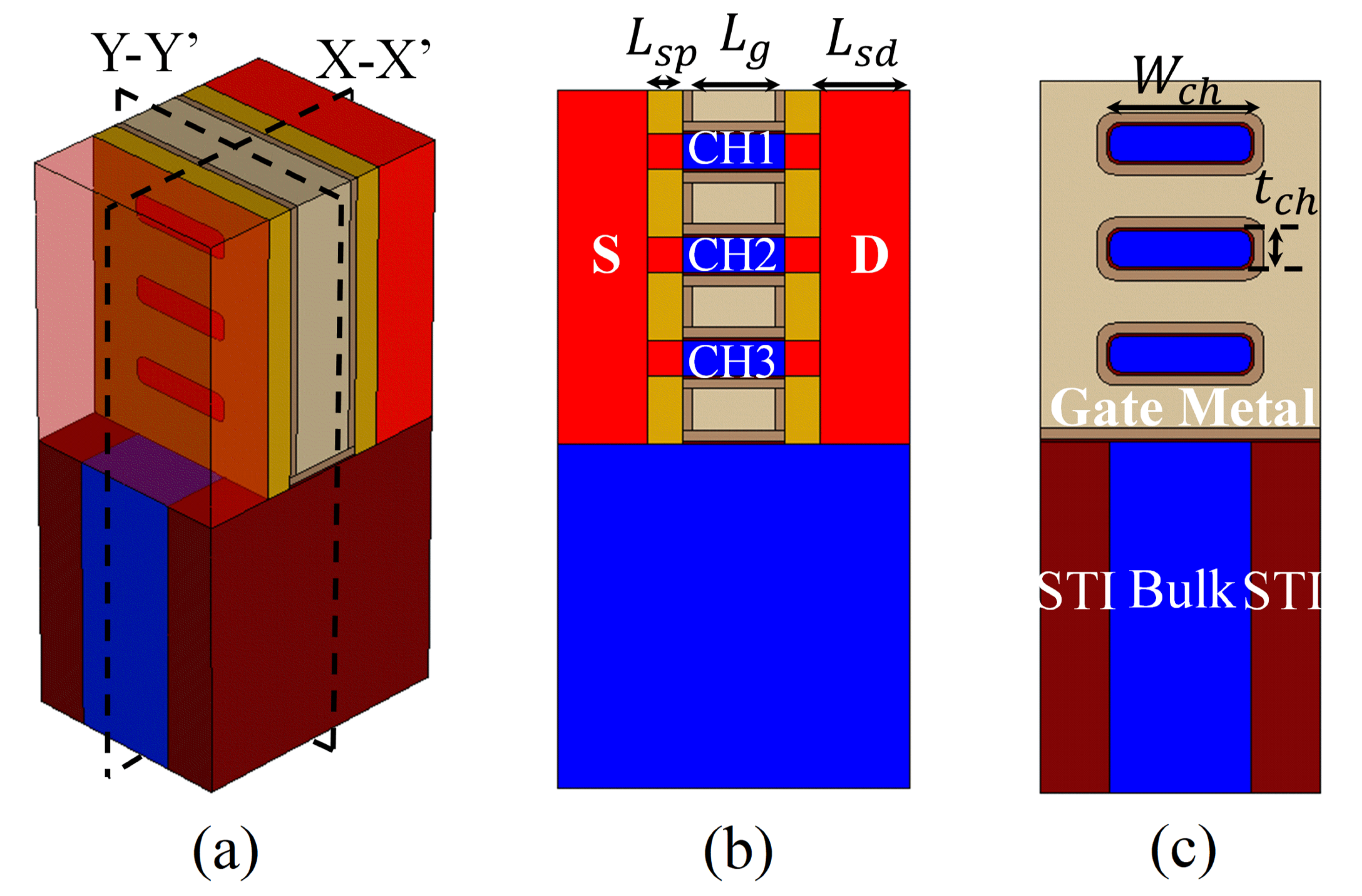
2.1. Device Structure

The 3-D schematic and 2-D cross-sectional views along and across the channel of the conventional 7-nm NSFET with punch through stopper (PTS) doping scheme, which is referred to in [19], are shown in Figure 1. The gate length ( L g ) and inner spacer length ( L s p ) are 12 and 5 nm, respectively. The S/D length is set to 13 nm. The vertical channel space ( N c h ) and channel thickness ( t c h ) are 10 and 5 nm, respectively. The doping concentrations of the channel and S/D region are 1 × 10 16 cm 3 and 1 × 10 20 cm 3 , respectively. Moreover, in order to reduce I O F F , the doping concentration of the PTS structure is 5 × 10 18 cm 3 . An effective-oxide-thickness (EOT) of 0.7 nm (0.45 nm SiO 2 and 1.5 nm HfO 2 ) is achieved. The source and drain contact resistance of NSFET is 1 × 10 9   Ω ·cm 2 . All the relevant physical parameters of the device are listed in Table 1.

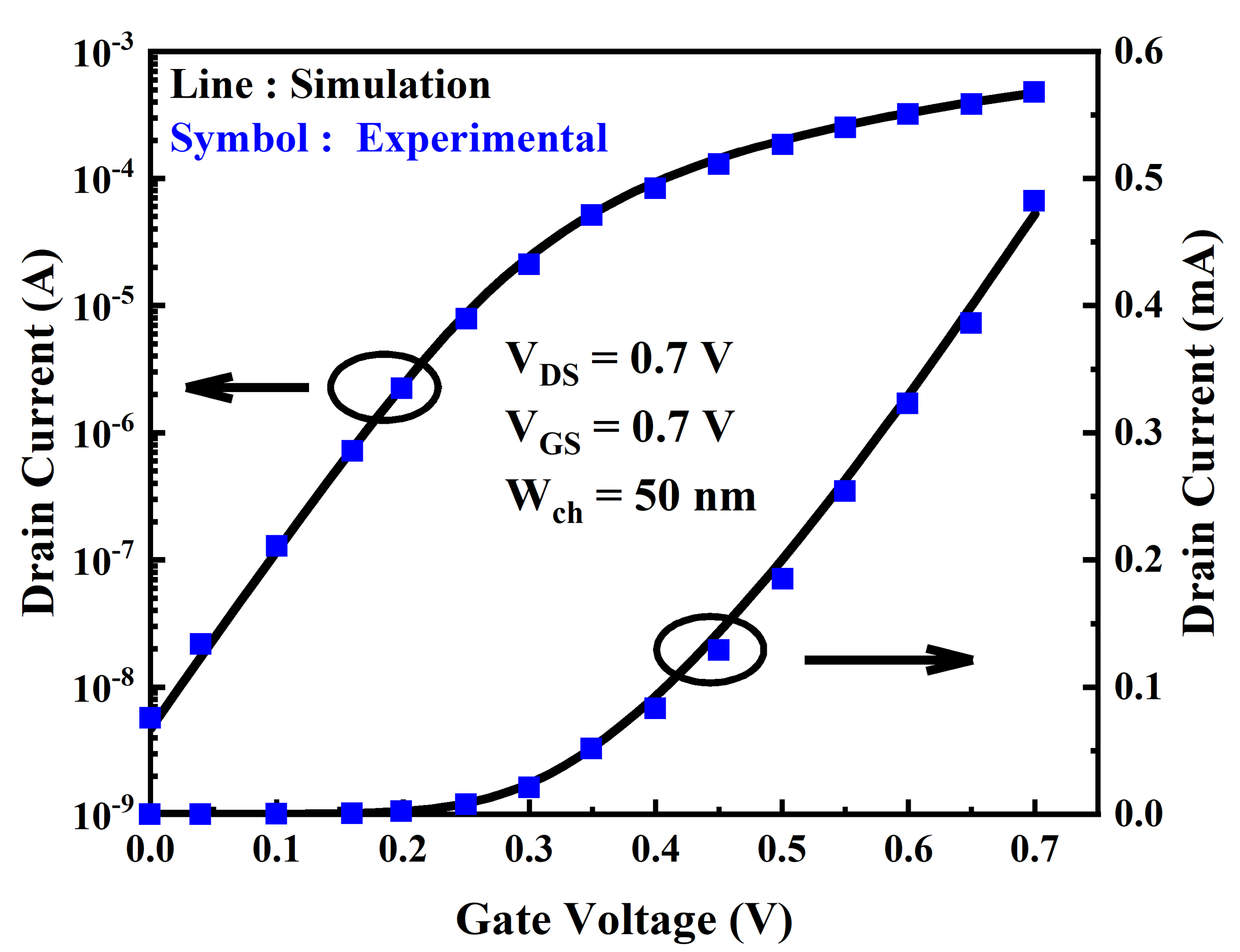
2.2. Simulation Settings

To ensure the accuracy of the following simulations, the physical parameters of NSFET are calibrated using the experimental data in [2]. According to the cross-sectional shapes given in [2], a similar structure was designed. In this calibration work, the channel had a rectangular cross-sectional shape with rounded corners, and the crescent inner spacer was also designed. The channel width is set to 50 nm to minimize the influence of the non-ideal channel cross-sectional shape on the NSFET performance. Figure 2 shows good calibration with the experimental data in the saturation regime. Here, we adjusted the channel doping concentration and the gate metal work function to control the OFF-state current ( I O F F ) in the subthreshold region. Then, we adjusted the high-field saturation model parameters to make the simulation results match the experimental data in the saturation region.
In addition, the density gradient quantization model is used to consider the quantum confinement effect of the nanosheets. The recombination models include Shockley–Read–Hall (SRH) and Auger models. In order to calculate the effective bandgap width, which determines the intrinsic density, the Bandgap Narrowing Slotboom Model was used. As the thickness of the nanosheet channel is only a few nanometers ( N c h = 5 nm), the mobility cannot be expressed with a typical field-dependent interface model. Thus, the thin-layer mobility and Lombardi models are applied to reflect the phonon and surface roughness scattering. The Doping Dependence model is specified to reflect the carrier-impurity scattering. The high field saturation model is also included to describe the carrier velocity saturation effect at high electric fields.
Finally, due to the different mobilities of the NS with (100) surface orientation and IB with (110) surface orientation, the parameter sets of the mobility model related to the surface orientation in TreeFET are adjusted [29,30,31,32]. After adjustment, the electron mobility and hole mobility of (110) are 0.9× and 1.3× of (100) [29], respectively. For areas that cause hybrid orientation, different sets of parameters are selected for simulation based on their spatial location, according to the nearest interface direction.

3. Results and Discussion
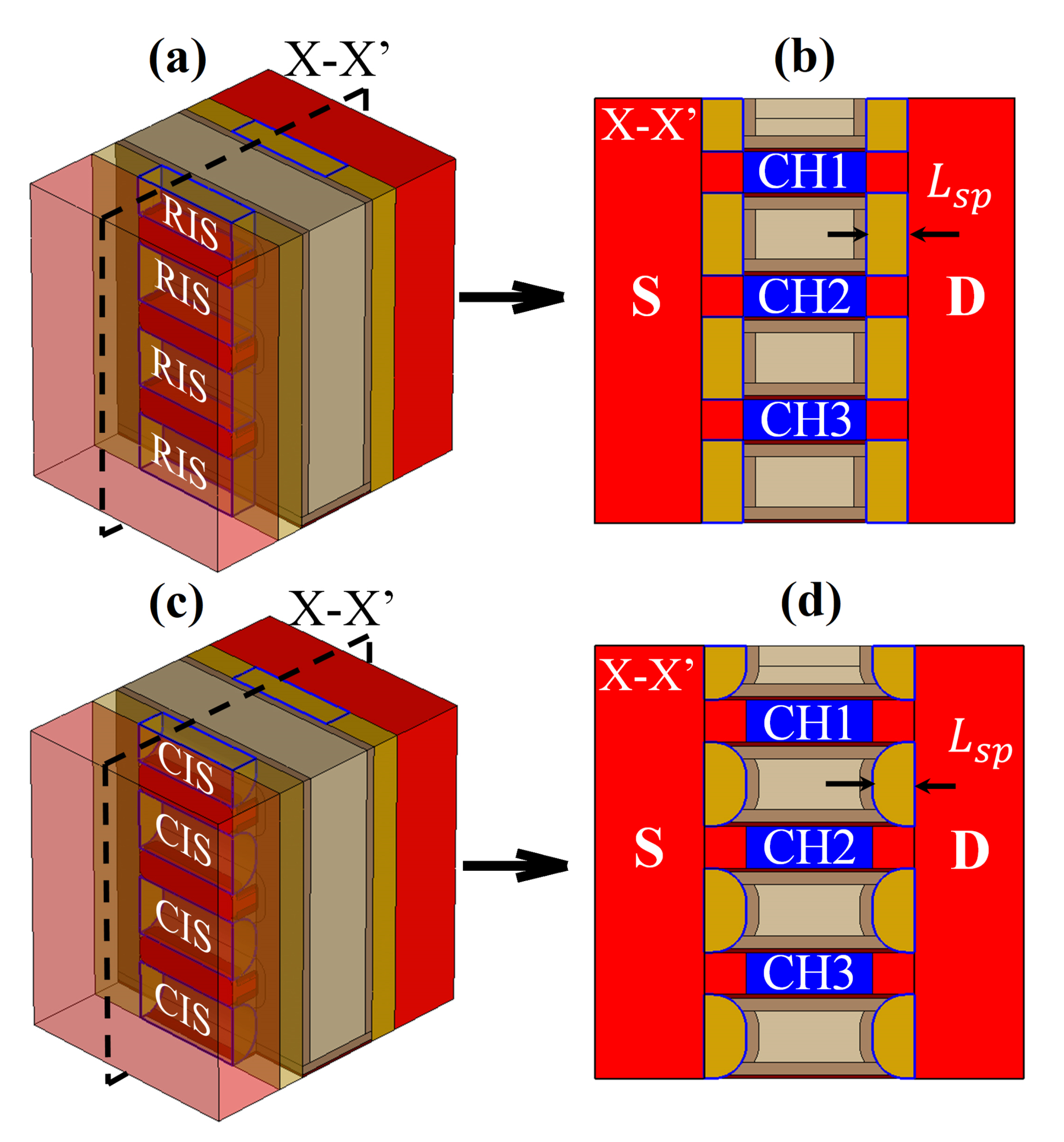
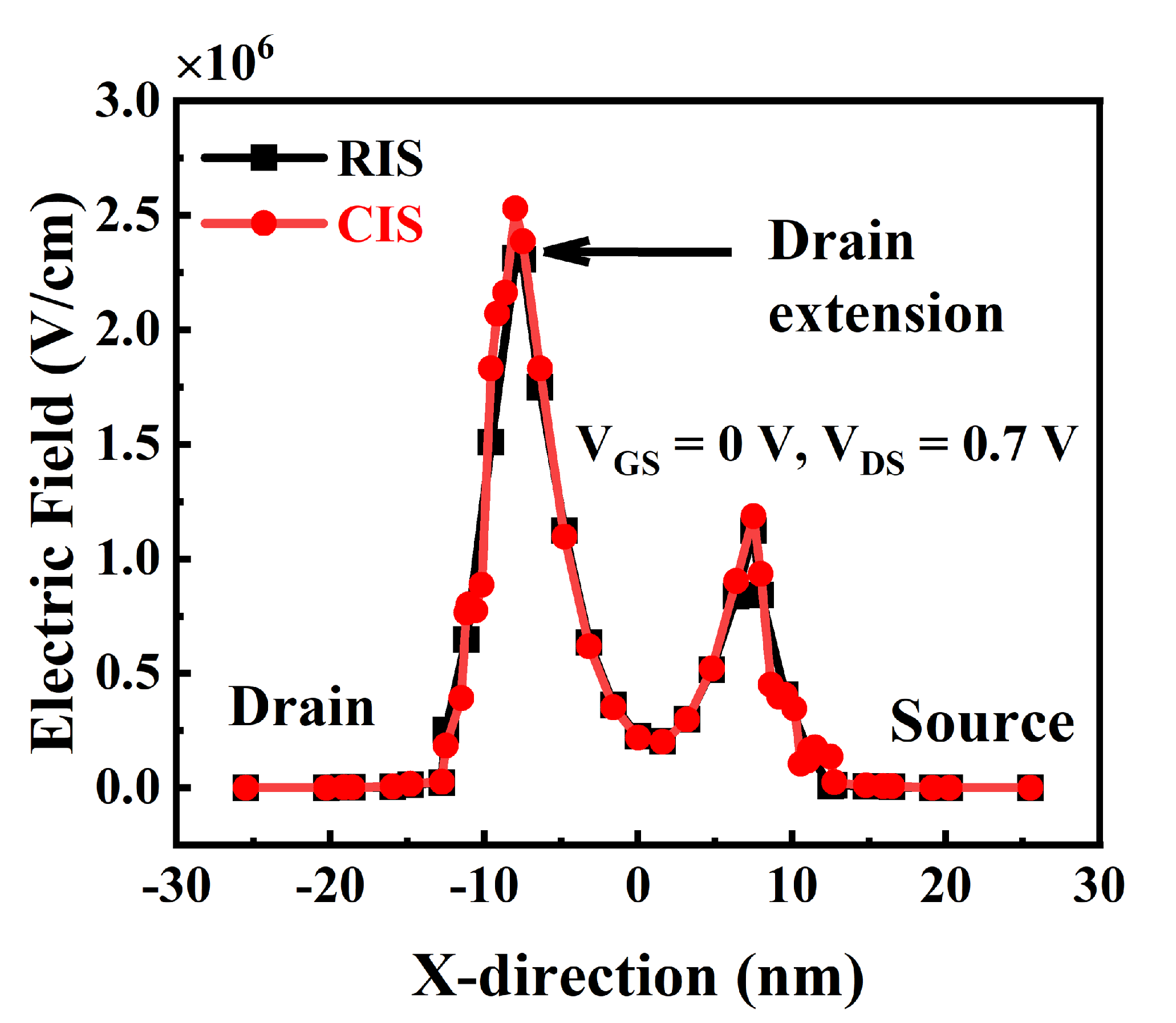
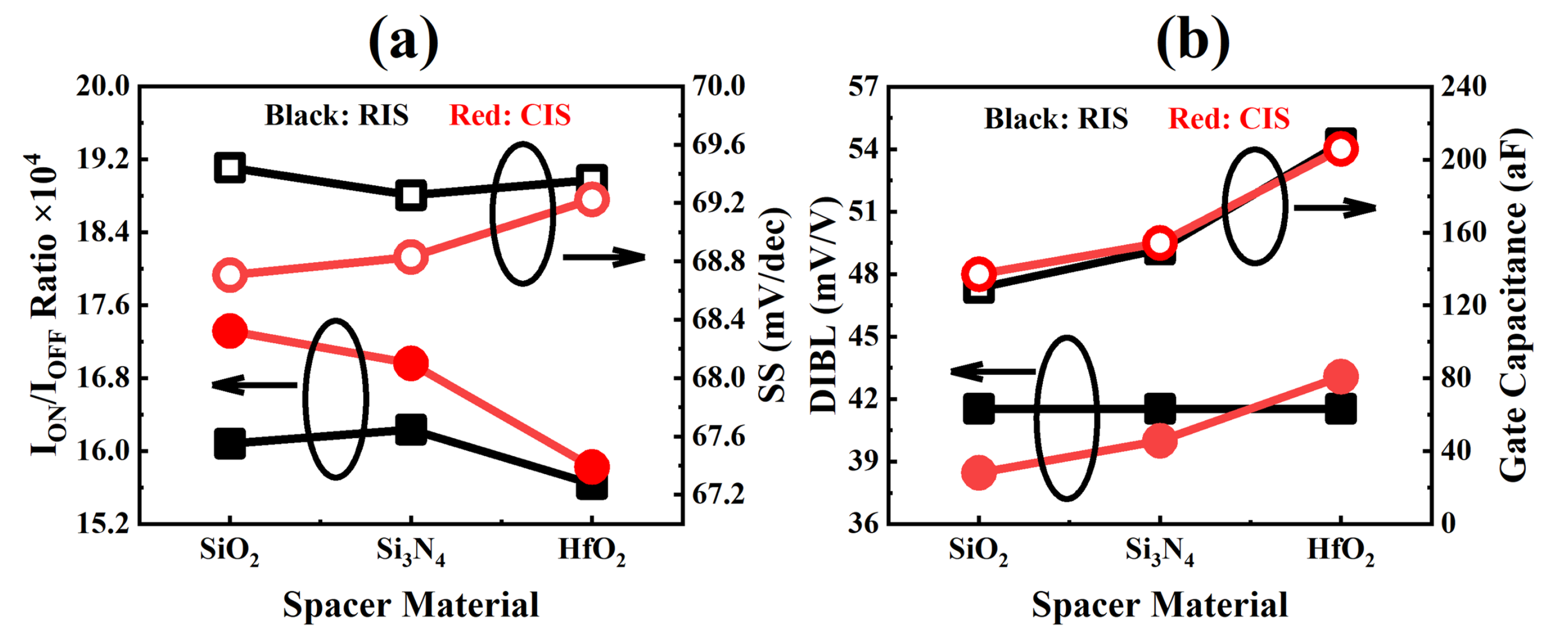
In this section, the effects of different cross-sectional shapes on the device characteristics are investigated. The Sentaurus TCAD is used to simulate the electrical characteristics of devices. I–V curves of all structures and significant electrical parameters are obtained. Here, the On-state current ( I O N ) is calculated at V G S = V D S = 0.7 V, while the OFF-state current ( I O F F ) is calculated at V G S = 0 V and V D S = 0.7 V [2]. The total gate capacitance ( C g g = I G × t/ V G S , and the I G is the gate displacement current under a time-dependent gate voltage) is calculated at V G = 0.7 V and V S = V B = V D = 0 V. A critical parameter that represents SCE is the drain-induced barrier lowering (DIBL), which can be calculated from the following equation [33,34]:
D I B L = V t l i n V t s a t V D s a t V D l i n
The DIBL effect is related to the threshold voltage definition. Here, the threshold voltage ( V t h ) is extracted by the constant current method. The V t s a t is the threshold voltage calculated in the saturation region ( V t s a t = V G S when the V D S = V D s a t = 0.7 V and the I D S = 100 nA × W e f f / L g ), and V t l i n is the threshold voltage calculated in the linear region ( V t l i n = V G S when the V D S = V D l i n = 0.05 V and the I D S = 100 nA × W e f f / L g ).

3.1. Inner Spacer

In previous TCAD simulations, the traditional rectangular inner spacer (RIS) is common [19,20,21], as shown in Figure 3a,b. However, a crescent inner spacer (CIS) can be formed due to the insufficient etching selectivity in the actual process [14,15,16,17], as shown in Figure 3c,d. To investigate how the non-ideal inner spacer cross-sectional shape impacts the performance of NSFET, the electrical characteristics of NSFET with RIS and CIS are simulated at different L g . In this work, we change the L g from 8 to 16 nm (meanwhile, the L s p is changed from 7 to 3 nm), keeping the total length of the L g plus the L s p fixed.
The comparison of the NSFET with a CIS and the NSFET with a RIS is analyzed under varying L g , as shown in Figure 4. From Figure 4a, it is observed that the NSFET with a CIS has a higher I O N / I O F F ratio than NSFET with a RIS. The increased trend slows down with L g increasing, showing improvements of 11.1%, 4.5%, and 2.4%, respectively. The I O N / I O F F ratio increases for NSFET with a CIS compared to NSFET with a RIS because the CIS improves the I O N and decreases the I O F F . Since the total length of the L g plus the L s p is fixed, the smaller is the L g , the weaker is the gate control capability, leading to a significant difference in the impact of CIS on NSFETs under varying L g . Figure 4b,c show that the subthreshold swing (SS) and drain-induced barrier lowering (DIBL) of the NSFET with a CIS are improved compared to the NSFET with a RIS. These results are consistent with the short-channel effects improvement due to the CIS increasing the effective gate length [6]. It also can be seen that the CIS has a more significant effect on the SS and DIBL with the smaller L g . The reason for the trend of SS is that the CIS has a more significant improvement in I O N , with the L g decreasing. For the trend of DIBL, the reason is that the CIS has a more significant enhancement in the gate control capability with the smaller L g . As shown in Figure 4d, the NSFET with a CIS has a larger C g g than the NSFET with a RIS. The phenomenon occurs because the CIS causes the high-k dielectric and gate to extend towards the junction region, increasing the outer-fringing field at the junction [Figure 5]. Then, the parasitic capacitance increases [22,23]. However, the C g g variation caused by CIS increases due to the enhancement in the increased trend of the gate fringing electric field, with L g increasing. Therefore, the non-ideal cross-sectional shape of the inner spacer has a significant impact on NSFET.
Moreover, many studies have demonstrated that the inner spacer material impacts the electrical characteristics of the NSFET [19,20]. We also studied the performance difference between CIS and RIS of various materials. Figure 6 displays the relevant simulation results. The NSFET with a CIS exhibits a higher I O N / I O F F ratio, smaller SS and DIBL, and larger C g g for both SiO 2 and Si 3 N 4 . The results for HfO 2 are not quite the same as SiO 2 and Si 3 N 4 . The NSFET with a CIS has a degraded DIBL and smaller C g g . This is because the coverage of HfO 2 layer of CIS is smaller than RIS, showing a lower outer fringing electric field. Therefore, the material also affects the effect of CIS on NSFET.

3.2. Stacked NS Channel

In the channel release process, the excessive etch can cause the loss of Si and form a tapered channel cross-sectional shape [28]. Figure 7a,b show the 3-D structure and X-X view of a 7-nm node NSFET with a tapered stacked NS channel cross-sectional shape, designed following the experimental work in [28]. Here, the rounding corner is introduced to reduce the corner effect of the device in the simulation. The parameter g is defined as the channel thickness ( t c h ), and the parameter e represents the thickness of Si at the end of the channel. The ideal channel cross-sectional shape is indicated by e/g = 1.0. Figure 7c illustrates the I O N and the I O F F at varying e/g ratios when W c h = 20 nm. It is shown that the non-ideal channel cross-sectional shape has a significant impact on NSFETs. As the e/g changes from 1.0 to 0.2, the I O N and the I O F F decrease from 193.8 to 132.8 µA and 1.22 to 0.3 nA, respectively, resulting in a reduction of 31.5% and 75.3%, respectively. This phenomenon occurs because the smaller is the e/g ratio, the larger is the loss of Si at the edge of the channel. Therefore, the device current decreases with a smaller e/g ratio due to the reduction in conduction area. In addition, the I O F F due to SCEs is also reduced, resulting in a significant degradation in I O F F than I O N .
The non-ideal cross-sectional shapes are mainly formed in the initial stage of the etching process and do not vary with the etching time [16]. Therefore, the channel width ( W c h ) also impacts the effect of the non-ideal channel cross-sectional shape on NSFET. Figure 8 shows the electrical characteristics of NSFETs with different e/g ratios at varying W c h from 20 to 40 nm. Since the effective channel width ( W e f f ) is insensitive with the e/g ratio varying when the W c h is large enough, the effect of the non-ideal channel cross-sectional shape on NSFETs becomes insignificant with the W c h increasing. Figure 8a plots the I O N / I O F F ratio variation with NS width. It can be seen that the NSFET with a smaller e/g ratio provides a larger I O N / I O F F ratio at a fixed channel width. For example, the I O N / I O F F ratio with an e/g ratio of 0.2 is 177.7% higher than that of conventional NS when W c h = 20 nm. This increased trend for I O N / I O F F can be explained by the fact that the I O F F decreases faster than the I O N , with the e/g falling. As the W c h increases, the I O N / I O F F ratio with an e/g ratio of 0.2 decreases by 68.5% at W c h = 40 nm compared with that at W c h = 20 nm. This reduction in drain current can be explained by the trend of SS with W c h varying, as shown in Figure 8b. As the W c h increases, the I O N increases slightly due to the increase in SS, while the I O F F increases due to the enlargement in the conduction area. The SS and DIBL are improved with a smaller e/g ratio, as shown in Figure 8b. These improvements are because the short-channel effects (SCEs) can be alleviated by reducing the channel width [35]. Figure 8c shows that the threshold voltage ( V t h ) of the tapered NS is increased by 16.6% over that of the conventional NS due to the lower I O N . The conduction area increases with W c h increasing. So, the increase of W c h would result in a reduction in the threshold voltage. Figure 8d indicates that the NSFET with conventional stacked NS channels presents a larger maximum transconductance ( g m , m a x ) value than the tapered NS channel. This is because the former has a larger W e f f . Therefore, the tapered NS improves the SCEs but sacrifices the driving current, resulting in an improvement in I O N / I O F F ratio, SS, and DIBL, but a degradation in V t h and g m , m a x .

3.3. Fin-Shaped IB Channel

The TreeFET structure is proposed to balance the electron and hole mobilities for CMOS devices [31]. It also enhances the device current compared to NSFET [29,30,31,32]. However, the presence of the IB significantly impacts TreeFET performance due to the insufficient etching selectivity. In order to investigate how the non-ideal cross-sectional shapes impact the TreeFET performance, we designed similar cross-sectional shapes based on the cross-sectional shapes given by the existing experimental results in [31], as illustrated in Figure 8. The 3-D scheme and the ideal Y-Y’ view of the TreeFET are depicted in Figure 9a,b. The height of IB ( H I B ) is 20 nm, and the width of IB ( W I B ) is 5 nm. The rest of the relevant parameters are consistent with the NSFETs listed in Table 1.
Two factors will result in a non-ideal channel cross-sectional shape of the TreeFET. The first factor is that the fin angle can cause the W c h and W I B at the bottom to be wider than that at the top, as shown in Figure 9c. Here, the top width of CH1 for all schemes is fixed at 20 nm, while the rest widths of channels vary with the fin angle from 0° to 4°. A fin angle of 0° represents the conventional cross-sectional shape. The second factor is that the insufficient etch can form a concave arc IB during the channel release, as shown in Figure 9d. In this case, the IB can be wider near the NS. Here, the parameter m is defined as the width of IB at the intersection, whereas the parameter t represents the ideal width of IB. The t/m = 1.0 is the ideal cross-sectional shape. To accurately analyze the effect of the corresponding factor on TreeFET performance, in this work, we discussed the two factors separately.
Figure 10 shows the influence of the above two factors on TreeFET performance at different W I B . As expected, the I O N / I O F F ratio, SS, and DIBL all deteriorate with W I B increasing. The two non-ideal factors have a more significant impact on electrical characteristics as the W I B increases. These results are because the gate control capability degrades with W I B increasing [3].
As the fin angle increases, the W c h and W I B increase, increasing the device current. However, the I O F F rises faster than the I O N . So, the I O N / I O F F ratio decreases as the fin angle changes from 0° to 4°, reaching 92.9% at W I B = 5 nm, as shown in Figure 10a. The larger W c h can degrade the electrostatic control behavior [6]. Also, the larger W I B reduces the gate control capability due to the smaller area-volume ratio of the channel region [3]. As shown in Figure 10b,c, these two cooperative phenomena eventually lead to the SS and DIBL all deteriorating as the fin angle varies from 0° to 4°, with the degradation reaching 23.4% and 69.6%, respectively, at W I B = 5 nm. Therefore, due to the rapid decrease in gate control capability, the fin angle increases from 0° to 4°, SCEs degradation is severe compared to the conventional TreeFET.
The smaller t/m is, the wider is the IB near NS, causing the current conduction area to increase. In this case, both I O N and I O F F increase, but I O F F rises dramatically, leading to a 79.9% decrease in the I O N / I O F F ratio at W I B = 5 nm, as shown in Figure 10d. As t/m decreases, SS and DIBL degrade by 19.3% and 50.0%, respectively, at W I B = 5 nm, as illustrated in Figure 10e,f. This is because the gate is further away from the intersection due to the wider IB near the NS, which reduces the gate control capability [30]. Therefore, the concave arc IB also causes a severe degradation in gate control capability. For the TreeFET with a concave arc IB, the I O N / I O F F ratio, SS, and DIBL all deteriorate compared to the conventional TreeFET.

4. Conclusions

In this article, the effects of non-ideal cross-sectional shapes of the inner spacer (IS), nanosheet (NS), and inter-bridge (IB) are investigated. The results show that the geometry and material of the inner spacer have significant effects on the performance of the NSFET. Compared with the rectangular inner spacer (RIS), the low-k crescent inner spacer (CIS) enhances the gate control capability while the high-k CIS degrades the drain-induced barrier lowering ( D I B L ) and reduces the gate capacitance ( C g g ). When the e/g = 0.2 and W c h = 20 nm, the tapered NS shows the best on/off current ratio ( I O N / I O F F ) with 177.7% improvement while increasing the threshold voltage by 16.6% over the rectangular NS. The TreeFET considering the fin angle and concave arc IB can degrade the gate control capability, and the SCEs degradation is severe compared to the ideal structure. When W I B = 5 nm, the degradation of I O N / I O F F , S S , and D I B L can reach 92.9%, 23.4%, and 69.6%, respectively, with fin angle increasing; The degradation of I O N / I O F F , S S , and D I B L can reach 79.9%, 19.3%, and 50.0%, respectively, with the t/m increasing. Moreover, the relevant parameters of each structure are well investigated, and the results show that the non-ideal cross-sectional shapes significantly impact device performance under smaller gate length ( L g ), narrower NS width ( W c h ), and wider IB width ( W I B ). To reduce the effect of non-ideal cross-sectional shapes on performance, geometry parameters including L g , W c h , and W I B should be set reasonably. Therefore, the detailed TCAD simulation results show that the non-ideal cross-sectional shapes should be considered to accurately determine the device’s electrical performance.

Author Contributions

Conceptualization, C.L. and M.J.D.; Data curation, H.L.; Formal analysis, H.Y.; Funding acquisition, C.L. and H.Y.; Investigation, F.K. and C.L.; Methodology, F.K., C.L. and M.J.D.; Project administration, C.L.; Software, H.L.; Supervision, C.L. and M.J.D.; Validation, F.K. and H.L.; Visualization, F.K.; Writing—original draft, F.K.; Writing—review and editing, F.K., C.L., H.Y. and M.J.D. All authors have read and agreed to the published version of the manuscript.

Funding

This research was funded in part by the cooperation project between Xidian University and Beijing Microelectronics Technology Institute, in part by the Project of Science and Technology on Reliability Physics and Application Technology of Electronic Component Laboratory (under Grant 6142806210302), in part by the China National Key R&D Program (Grant No. 2022YFF0605800), in part by the 111 Project of China.

Data Availability Statement

All data that support the findings of this study are included within the article.

Conflicts of Interest

The authors declare no conflict of interest.

References

  1. Lee, K.S.; Park, J.Y. Inner Spacer Engineering to Improve Mechanical Stability in Channel-Release Process of Nanosheet FETs. Electronics 2021, 10, 1395. [Google Scholar] [CrossRef]
  2. Loubet, N.; Hook, T.; Montanini, P.; Yeung, C.W.; Kanakasabapathy, S.; Guillom, M.; Yamashita, T.; Zhang, J.; Miao, X.; Wang, J.; et al. Stacked nanosheet gate-all-around transistor to enable scaling beyond FinFET. In Proceedings of the 2017 Symposium on VLSI Technology, Kyoto, Japan, 5–8 June 2017; pp. T230–T231. [Google Scholar] [CrossRef]
  3. Sun, Y.; Li, X.; Liu, Z.; Liu, Y.; Li, X.; Shi, Y. Vertically Stacked Nanosheets Tree-Type Reconfigurable Transistor with Improved ON-Current. IEEE Trans. Electron Devices 2022, 69, 370–374. [Google Scholar] [CrossRef]
  4. Wang, D.; Sun, X.; Liu, T.; Chen, K.; Yang, J.; Wu, C.; Xu, M.; Zhang, W.D. Investigation of Source/Drain Recess Engineering and Its Impacts on FinFET and GAA Nanosheet FET at 5 nm Node. Electronics 2023, 12, 770. [Google Scholar] [CrossRef]
  5. Yoon, J.S.; Jeong, J.; Lee, S.; Baek, R.H. Optimization of nanosheet number and width of multi-stacked nanosheet FETs for sub-7-nm node system on chip applications. Jpn. J. Appl. Phys. 2019, 58, SBBA12. [Google Scholar] [CrossRef]
  6. Kim, S.; Lee, K.; Kim, S.; Kim, M.; Lee, J.H.; Kim, S.; Park, B.G. Investigation of Device Performance for Fin Angle Optimization in FinFET and Gate-All-Around FETs for 3 nm-Node and Beyond. IEEE Trans. Electron Devices 2022, 69, 2088–2093. [Google Scholar] [CrossRef]
  7. Rathore, S.; Jaisawal, R.K.; Kondekar, P.N.; Bagga, N. Design Optimization of Three-Stacked Nanosheet FET from Self-Heating Effects Perspective. IEEE Trans. Device Mater. Reliab. 2022, 22, 396–402. [Google Scholar] [CrossRef]
  8. Liu, R.; Li, X.; Sun, Y.; Li, F.; Shi, Y. Thermal Coupling Among Channels and Its DC Modeling in Sub-7-nm Vertically Stacked Nanosheet Gate-All-Around Transistor. IEEE Trans. Electron Devices 2021, 68, 6563–6570. [Google Scholar] [CrossRef]
  9. Venkateswarlu, S.; Nayak, K. Hetero-Interfacial Thermal Resistance Effects on Device Performance of Stacked Gate-All-Around Nanosheet FET. IEEE Trans. Electron Devices 2020, 67, 4493–4499. [Google Scholar] [CrossRef]
  10. Yoo, S.; Kim, S. Leakage Optimization of the Buried Oxide Substrate of Nanosheet Field-Effect Transistors. IEEE Trans. Electron Devices 2022, 69, 4109–4114. [Google Scholar] [CrossRef]
  11. Lee, K.S.; Shin, W.C.; Yeon, J.W.; Park, J.Y. Impact of device-to-device interference in nanosheet field-effect transistors. Microelectron. Reliab. 2023, 145, 114995. [Google Scholar] [CrossRef]
  12. Santos, A.; Deen, M.J.; Marsal, L.F. Low-cost fabrication technologies for nanostructures: State-of-the-art and potential. Nanotechnology 2015, 26, 042001. [Google Scholar] [CrossRef] [PubMed]
  13. Mukesh, S.; Zhang, J. A Review of the Gate-All-Around Nanosheet FET Process Opportunities. Electronics 2022, 11, 3589. [Google Scholar] [CrossRef]
  14. Loubet, N.; Kal, S.; Alix, C.; Pancharatnam, S.; Zhou, H.; Durfee, C.; Belyansky, M.; Haller, N.; Watanabe, K.; Devarajan, T.; et al. A Novel Dry Selective Etch of SiGe for the Enablement of High Performance Logic Stacked Gate-All-Around NanoSheet Devices. In Proceedings of the 2019 IEEE International Electron Devices Meeting (IEDM), San Francisco, CA, USA, 7–11 December 2019; pp. 11.4.1–11.4.4. [Google Scholar] [CrossRef]
  15. Durfee, C.; Kal, S.; Pancharatnam, S.; Bhuiyan, M.; Otto, I., IV; Flaugh, M.; Smith, J.; Chanemougame, D.; Alix, C.; Zhou, H.; et al. Highly Selective SiGe Dry Etch Process for the Enablement of Stacked Nanosheet Gate-All-Around Transistors. ECS Meet. Abstr. 2021, MA2021-02, 943. [Google Scholar] [CrossRef]
  16. Zhao, Y.; Iwase, T.; Satake, M.; Hamamura, H. Formation Mechanism of a Rounded SiGe-Etch-Front in an Isotropic Dry SiGe Etch Process for Gate-All-Around (GAA)-FETs. In Proceedings of the 2021 5th IEEE Electron Devices Technology & Manufacturing Conference (EDTM), Chengdu, China, 8–11 April 2021; pp. 1–3. [Google Scholar] [CrossRef]
  17. Zhao, Y.; Iwase, T.; Satake, M.; Hamamura, H. Formation Mechanism of Rounded SiGe-Etch Front in Isotropic SiGe Plasma Etching for Gate-All-Around FETs. IEEE J. Electron Devices Soc. 2021, 9, 1112–1116. [Google Scholar] [CrossRef]
  18. Schmidt, D.; Cepler, A.; Durfee, C.; Pancharatnam, S.; Frougier, J.; Breton, M.; Greene, A.; Klare, M.; Koret, R.; Turovets, I. Development of SiGe Indentation Process Control for Gate-All-Around FET Technology Enablement. IEEE Trans. Semicond. Manuf. 2022, 35, 412–417. [Google Scholar] [CrossRef]
  19. Liu, R.; Li, X.; Sun, Y.; Shi, Y. A Vertical Combo Spacer to Optimize Electrothermal Characteristics of 7-nm Nanosheet Gate-All-Around Transistor. IEEE Trans. Electron Devices 2020, 67, 2249–2254. [Google Scholar] [CrossRef]
  20. Ryu, D.; Kim, M.; Kim, S.; Choi, Y.; Yu, J.; Lee, J.H.; Park, B.G. Design and Optimization of Triple-k Spacer Structure in Two-Stack Nanosheet FET from OFF-State Leakage Perspective. IEEE Trans. Electron Devices 2020, 67, 1317–1322. [Google Scholar] [CrossRef]
  21. Jeong, J.; Yoon, J.S.; Lee, S.; Baek, R.H. Novel Trench Inner-Spacer Scheme to Eliminate Parasitic Bottom Transistors in Silicon Nanosheet FETs. IEEE Trans. Electron Devices 2023, 70, 396–401. [Google Scholar] [CrossRef]
  22. Yoon, J.S.; Jeong, J.; Lee, S.; Baek, R.H. Punch-Through-Stopper Free Nanosheet FETs with Crescent Inner-Spacer and Isolated Source/Drain. IEEE Access 2019, 7, 38593–38596. [Google Scholar] [CrossRef]
  23. Lee, S.; Jeong, J.; Yoon, J.S.; Lee, S.; Lee, J.; Lim, J. Sensitivity of Inner Spacer Thickness Variations for Sub-3-nm Node Silicon Nanosheet Field-Effect Transistors. Nanomaterials 2022, 12, 3349. [Google Scholar] [CrossRef]
  24. Jegadheesan, V.; Sivasankaran, K.; Konar, A. Optimized Substrate for Improved Performance of Stacked Nanosheet Field-Effect Transistor. IEEE Trans. Electron Devices 2020, 67, 4079–4084. [Google Scholar] [CrossRef]
  25. Jegadheesan, V.; Sivasankaran, K.; Konar, A. Impact of geometrical parameters and substrate on analog/RF performance of stacked nanosheet field effect transistor. Mater. Sci. Semicond. Process. 2019, 93, 188–195. [Google Scholar] [CrossRef]
  26. Woo, S.; Jeong, H.; Choi, J.; Cho, H.; Kong, J.T.; Kim, S. Machine-Learning-Based Compact Modeling for Sub-3-nm-Node Emerging Transistors. Electronics 2022, 11, 2761. [Google Scholar] [CrossRef]
  27. Seon, Y.; Chang, J.; Yoo, C.; Jeon, J. Device and Circuit Exploration of Multi-Nanosheet Transistor for Sub-3 nm Technology Node. Electronics 2021, 10, 180. [Google Scholar] [CrossRef]
  28. Catano, C.; Joy, N.; Talone, C.; Sridhar, S.; Voronin, S.; Biolsi, P.; Ranjan, A. Peculiarities of selective isotropic Si etch to SiGe for nanowire and GAA transistors. In Advanced Etch Technology for Nanopatterning VIII; Wise, R.S., Labelle, C.B., Eds.; SPIE: Bellingham, WA, USA, 2019; Volume 10963, p. 109630E. [Google Scholar] [CrossRef]
  29. Tsen, C.J.; Chung, C.C.; Liu, C.W. Self-Heating Mitigation of TreeFETs by Interbridges. IEEE Trans. Electron Devices 2022, 69, 4123–4128. [Google Scholar] [CrossRef]
  30. Li, X.; Zhu, H.; Gan, W.; Huang, W.; Wu, Z. A Three-Dimensional Simulation Study of the Novel Comb-Like-Channel Field-Effect Transistors for the 5-nm Technology Node and Beyond. IEEE Trans. Electron Devices 2022, 69, 4786–4790. [Google Scholar] [CrossRef]
  31. Tu, C.T.; Hsieh, W.H.; Huang, B.W.; Chen, Y.R.; Liu, Y.C.; Tsai, C.E.; Chueh, S.J.; Liu, C.W. Experimental Demonstration of TreeFETs Combining Stacked Nanosheets and Low Doping Interbridges by Epitaxy and Wet Etching. IEEE Electron Device Lett. 2022, 43, 682–685. [Google Scholar] [CrossRef]
  32. Ye, H.Y.; Liu, C.W. On-Current Enhancement in TreeFET by Combining Vertically Stacked Nanosheets and Interbridges. IEEE Electron Device Lett. 2020, 41, 1292–1295. [Google Scholar] [CrossRef]
  33. Deen, M.; Yan, Z. DIBL in short-channel NMOS devices at 77 K. IEEE Trans. Electron Devices 1992, 39, 908–915. [Google Scholar] [CrossRef]
  34. Deen, M.; Yan, Z. Substrate bias effects on drain-induced barrier lowering in short-channel PMOS devices. IEEE Trans. Electron Devices 1990, 37, 1707–1713. [Google Scholar] [CrossRef]
  35. Wu, Y.T.; Chiang, M.H.; Chen, J.F.; Liu, T.J.K. Simulation-Based Study of High-Permittivity Inserted-Oxide FinFET With Low-Permittivity Inner Spacers. IEEE Trans. Electron Devices 2021, 68, 5529–5534. [Google Scholar] [CrossRef]
Figure 1. (a) 3-D view, (b) X-X’ view, and (c) Y-Y’ view of the conventional 7-nm NSFET with PTS doping scheme.
Electronics 12 03419 g001
Figure 2. The calibration of I d V g curve of the NSFET ( W c h = 50 nm) with experimental data from [2] in the saturation regime.
Electronics 12 03419 g002
Figure 3. (a) 3-D structure, and (b) X-X’ view of the NSFET with Rectangular Inner Spacer (RIS). (c) 3-D structure, and (d) X-X’ view of the NSFET with Crescent Inner Spacer (CIS).
Electronics 12 03419 g003
Figure 4. Trend of (a) I O N / I O F F ratio, (b) SS, (c) DIBL, and (d) C g g of NSFET with a rectangular inner spacer compared with the NSFET with a crescent inner spacer under different L g .
Electronics 12 03419 g004
Figure 5. Electric field along the x-direction according to the cross-sectional shape of inner spacer when the V G S = 0 V, the V D S = 0.7, and the L g = 12 nm.
Electronics 12 03419 g005
Figure 6. Comparison of (a) I O N / I O F F ratio and SS, (b) DIBL and C g g between NSFET with a rectangular inner spacer and NSFET with a crescent inner spacer of different materials.
Electronics 12 03419 g006
Figure 7. (a) 3-D structure, and (b) Y-Y’ view of the NSFET with a tapered channel cross-sectional shape. (c) drain current of NSFETs at varying e/g ratios when W c h = 20 nm.
Electronics 12 03419 g007
Figure 8. Trend of (a) I O N / I O F F ratio, (b) SS, (c) DIBL and, (d) g m , m a x of NSFETs with different e/g ratios considering different NS width ( W c h ).
Electronics 12 03419 g008
Figure 9. (a) 3-D view, and (b) ideal Y-Y’ view of TreeFET. (c) Y-Y’ view of TreeFET considering fin angle. (d) Y-Y’ view of TreeFET with concave arc IB.
Electronics 12 03419 g009
Figure 10. The influence of fin angle on (a) I O N / I O F F ratio, (b) SS and (c) DIBL at varying IB width. The effect of concave arc IB on (d) I O N / I O F F ratio, (e) SS and (f) DIBL at different IB width.
Electronics 12 03419 g010
Table 1. Device parameters.
ParametersValues
Gate length, L g 12 nm
Spacer length, L s p 5 nm
Source/Drain length, L s d 13 nm
Contact gate pitch, CGP48 nm
Channel width, W c h 20–50 nm
Channel thickness, t c h 5 nm
Vertical channel space, N c h 10 nm
Equivalent oxide thickness, E O T 0.7 nm
Channel doping, N c h a n n e l 1 × 10 16 cm 3
Source/Drain doping, N S D 1 × 10 20 cm 3
PTS doping, N b u l k 5 × 10 18 cm 3
Contact resistance 1 × 10 9 Ω ·cm 2
Disclaimer/Publisher’s Note: The statements, opinions and data contained in all publications are solely those of the individual author(s) and contributor(s) and not of MDPI and/or the editor(s). MDPI and/or the editor(s) disclaim responsibility for any injury to people or property resulting from any ideas, methods, instructions or products referred to in the content.

