Article

Control and Implementation of the Parallel Enhanced Commutation Integrated Nested Multilevel Inverter Topology

Research Group Electromobility and Learning Systems, Technische Hochschule Ingolstadt, D-85049 Ingolstadt, Germany
*
Author to whom correspondence should be addressed.
Electronics 2023, 12(14), 3130; https://doi.org/10.3390/electronics12143130
Submission received: 19 June 2023 / Revised: 5 July 2023 / Accepted: 13 July 2023 / Published: 19 July 2023

Abstract

:
Due to their high efficiency and advanced battery management capability, cascaded multilevel inverters are an exciting option for battery electric powertrains. A promising, new and highly efficient cascaded multilevel inverter is the Parallel Enhanced Commutation Integrated Nested Multilevel Inverter. The inverter, with four semiconductor switches per submodule, can reconfigure individual battery cells in series and parallel and generate positive and negative phase voltages in regular four-quadrant operation. Therefore, emerging degrees of freedom in battery management and inverter operation must be managed and mapped into a specific Switching State for every switch. As controlling the high number of switches is safety-relevant, this publication profoundly explains the inverter’s functionality. We introduce a Switching Function that accepts easy-to-understand functional states as input, simplifying research on higher-level control algorithms and advanced single-cell battery-management capabilities. As the Switching Function guarantees safe operation and the correct contribution of every cell to the overall functionality of the inverter, it enables researchers to confidently use and thereby accelerate research on the promising new topology. The method we describe is fast, simple, deterministic and designed to convert setpoint specifications into an executable Switching Pattern. We prove that our Switching Function is operable on an FPGA with a twenty-kilohertz setpoint update operating a 17-level inverter.

1. Introduction

The field of e-mobility has seen a huge upswing and massive investment in recent years, as the race is on for the drive technology of the future. Battery Electric Vehicles (BEVs) are currently seen as the favoured solution and are being focused on by politicians and industry.
Nowadays, the traction battery of these BEVs consists of many battery cells electrically connected in series and parallel to form a battery system [1]. This is the only way to achieve high output voltage and the energy content required by traction applications with prevailing lithium-ion battery technology [2]. Due to the rigid interconnection of the battery cells, there is a fixed DC output voltage at the terminals of the battery system. To generate the frequency- and amplitude-adjustable AC voltage required by the three-phase motors used in BEVs, a two-level inverter is currently connected between the battery system and the electrical machine. Since the two-level inverter only has one DC voltage source available, it cannot set any intermediate voltage values between the positive and negative DC-Link voltage directly. To achieve variable voltages in frequency and amplitude, methods of Pulse Width Modulation (PWM) and the filtering effect of ohmic-inductive loads are needed [3]. These methods can be used to generate a pulse-modulated voltage that has a similar effect on the resulting current as a comparable sinusoidal AC voltage. The required high switching frequencies are in the kilohertz range and lead to high switching losses. However, even with these high switching frequencies harmonic contents in the current and torque of the electrical machine are not avoidable and unwanted effects of electromagnetic interference arise [2,3,4].
An interesting enhancement of the two-level inverter is the Multilevel Inverter (MLI). MLIs were known from high-voltage high-power applications. In this area, conventional two-level inverters cannot be used due to the limited voltage ratings of the current semiconductor technology [5,6,7]. However, in addition to its traditional field of application, recently the usage of MLIs in the field of renewable energies for low-voltage applications has been investigated. The MLI idea is to intrinsically have several voltage levels. If a specific voltage value is demanded by a controller, the MLI can approximate the desired voltage by choosing the most suitable available voltage level [8]. Therefore, even with a comparatively small number of levels, PWM can be wholly dispensed with. As a result, lower switching losses, lower harmonic content and higher efficiency are to be expected compared to conventional two-level IGBT or MOSFET inverters, as suggested by the studies [9,10,11,12]. However, with MLIs, many individual switching elements must be operated. At the same time, correct and deterministic switching behaviour is crucial to guarantee safe operation, correct output voltage and exact execution of the battery-management requirements. The Parallel Enhanced Commutation Integrated Nested (PECIN) MLI, in particular, has a high functional density where dedicated control mechanisms are required if the inverter’s full functionality is to be used. Since switching device control is safety-critical and essential to MLI usability, a structured and easy-to-use Switching Function is provided within our publication.
The parts of the paper are structured according to the following description. Section 2 introduces the idea of battery electric cascaded MLIs and, as a member of this family, the PECIN MLI, which is the subject of this publication. Therefore, Section 3 provides a fundamental analysis of the PECIN topology, as a deep understanding is critical to deriving the control scheme. It includes a detailed study of the principle of operation with examples and an explanation of state-of-the-art control techniques from the literature. Thereupon, the general idea of the Switching Function is derived. First, the inputs of the Switching Function are discussed since their understanding is essential for a later application of the Switching Function and, thus, the usability of the PECIN topology in general. After that, the complete process to derive a Switching Pattern from the input is presented, resulting in a fully functional Switching Function. Finally, Section 4 presents an optimisation of the Switching Function from Section 3. The implementations from Section 3 and Section 4 provide the same results since they are based on the same principle. However, the algorithm from Section 4 focuses on execution performance and can be implemented very efficiently on an FPGA. Section 4 results in the final Switching Function. In Section 5, experimental validation for the Switching Function is provided.

2. Cascaded Multilevel Inverters

Cascaded MLIs are promising candidates for BEVs due to their modular approach and the resulting good scalability. Within a cascaded MLI, several voltage sources with smaller output voltages are connected via an electrical network to achieve multiple voltage levels and the high output voltage of the MLI. A core aspect of a cascaded MLI is that the electrical network consists of a recurring structure. Thus, recurring electrical circuitry and energy storage can be combined into one submodule (SM) [7,13,14]. By simply stringing these SMs together, a phase string with any number of levels can be constructed.
The electrical network consists of different power paths with switches that can be activated to create and dissolve connections between the voltage sources during operation. By activating specific switching combinations, different voltage levels can be directly provided at the terminals of the inverter [8,15]. Due to the resulting low switching effort in combination with the low-voltage MOSFET technology, the MLI approach promises maximum efficiency, especially in the partial load range where BEVs are most often operated [9,10,11,12].

2.1. Cascaded Multilevel Inverters as Reconfigurable Batteries

The MLI becomes a reconfigurable battery system if battery cells are used as voltage sources [7,9,15,16]. Here, the traction batteries of BEVs in particular are suitable for the construction of cascaded MLIs since many individual and galvanically isolated voltage sources, the incorporated battery cells, are already present [9,12,13,17]. In such a system, energy storage and inverter are merged into one system, a battery electric MLI.
In conventional battery systems, Battery Management System (BMS) cannot intervene in the operation of the individual battery cells due to the rigid connection of the battery cells and the performance of the entire battery system is limited by the weakest individual cell. In addition to improved inverter performance, the reconfiguration capability of the MLI can be used to manipulate the operation of individual battery cells to perform BMS tasks such as balancing [13,16,18,19,20,21,22], bad-block management [23] and advanced cell monitoring through reconfiguration [23,24,25,26].
The battery electric MLI can provide AC voltage with adjustable amplitude and frequency and DC voltage with adjustable amplitude. These abilities make the battery electric MLI suitable as variable-speed drives in four-quadrant operation and for direct bidirectional AC or DC charging of incorporated battery storage without additional charging electronics, e.g., in grid-connected applications [27,28,29]. In addition, the MLI enables dedicated single-cell battery management by reconfiguration during load operation without affecting load operation. The opportunities to leverage synergies in inverter performance and battery-management capabilities make the battery electric MLI a promising candidate for future propulsion technology [9,10,12,15,17].

2.2. PECIN MLI

For the practical implementation of the battery electric cascaded MLI concept, many different electrical circuits with various scopes of functions have been developed in recent years [15,30,31]. These circuits, referred to as topologies, have different capabilities and differ in performance and efficiency [10,32].
An up-and-coming candidate in functional scope and efficiency is the PECIN MLI presented in [32]. The PECIN MLI offers inherent commutation capability and serial and parallel reconfiguration, focusing on the lowest possible internal circuit resistance. Therefore, it excels in efficiency compared to other MLI topologies [32]. At the same time, it provides full single-cell battery-management capability and retains a reduced amount of required electronic components compared to its functional range [32,33]. A comprehensive analysis of the PECIN MLI, its development process, an efficiency analysis and a comparison to state-of-the-art MLI topologies can be found in [32]. A PECIN MLI can be built out of A phase arms. Typically, A = 3 for traction applications, e.g., to operate a three-phase induction motor. A phase arm comprises the PECIN topology and can incorporate N cells. For clarity, a single PECIN MLI phase arm with N = 4 cells is presented in Figure 1. The investigated PECIN MLI would thus consist of N·A = 12 cells in a three-phase setup. Since the functional principle is the same for all phase arms, only one will be considered in the following. In Figure 1, this phase arm has a different Switching Pattern in subfigure a–c. These Switching Patterns result in the load paths shown as examples, based on which some primary considerations and an introduction to the functional scope of the topology will be presented in the following.
The PECIN MLI is considered a symmetric MLI; therefore, the built-in battery cells are of the same type [32]. Two consecutive cells within the topology are connected via four powerlines, each containing a switching device. The basic principle is that the cell terminals of one cell are directly connectable to both output terminals of the previous and subsequent cell. With these powerlines, it is possible to connect an anode or a cathode of a cell to a cathode or an anode of the preceding or following cell to create an electric series connection of cells (cf. Figure 1c). Therefore, the PECIN MLI is bidirectional and can intrinsically generate positive and negative output voltages between the phase string terminals {N,L}. A PECIN MLI with N incorporated cells can thus provide L = 2N + 1 different output voltage levels. In addition to regular four-quadrant operation, connecting the anodes and cathodes of a series of consecutive cells is possible to connect them electrically in parallel (cf. Figure 1a Z2, Z3 and Z4). This functionality can, e.g., be used to distribute load current among parallel cells and effectively reduce the internal resistance of the battery system and thus the conduction losses of the inverter [32]. Furthermore, cell individual bypassing is possible at any time by passing through the network so that bypassed cells are only electrically connected to the load path on one terminal (cf. Figure 1b Z2 and Z3). Therefore, single-cell battery-management capability is provided as the connection of cells decides which cells are operated and which cells are idle [15]. Because of low switching and conduction losses, the MOSFET technology is a suitable choice for the switching elements [10,12]. One disadvantage of the MOSFET that comes into play with the PECIN topology is that it is only unidirectionally blocking. However, the PECIN design needs switches with unidirectional and switches with bidirectional blocking capability [32]. For unidirectional blocking switches, a single MOSFET can be used (cf. Figure 1: M1–M10), while for the bidirectional blocking switches, Back-to-Back (BtB) MOSFETs in common source configuration are suitable (cf. Figure 1: B1–B8). In this configuration, the BtB and the single MOSFET can be treated like ideal switches with discrete ’on’- and ’off’-states to develop the control scheme. However, a BtB MOSFET has twice the internal resistance of a single MOSFET. As a result, the PECIN MLI has traces with different line resistances. A good control procedure takes this characteristic into account to operate the inverter at its highest possible efficiency [32].

3. Elaboration of the PECIN Switching Function

While the control of the few switches in the conventional two-level inverter is simple, the sheer number of semiconductor switches in the MLI makes the control and management of the switches a demanding task. Every switch {B1,…,B2N, M1,…,M2N+2} must be applied with an individual control signal. The sequence of control signals must ensure that a valid current path is created between the terminals {N,L} of the inverter and that short circuits of cells are safely prevented.
However, since the PECIN topology has a high density of functions compared to the number of installed traces and switching elements, the paths are assigned with multiple functions and multiple dependencies between switching operations must be considered. For example, activating switch B7 in Figure 1b leads to a short circuit of the cell Z4, while in Figure 1c it represents a valid switching position. In addition, even if a valid and save load path can be established, several options are available to create a path for similar output functionality [33]. For example, the valid load paths presented in Figure 1a–c deliver the same output voltage between their phase terminals {N,L}, even if they all use a different switching pattern. In addition, they assign different operating states to the individual cells. In Figure 1a, Z3 is in parallel with Z2 and Z4 and the cell compound delivers a positive load current IL. However, Z3 is idle in Figure 1b and even carries a negative current in Figure 1c. Therefore, on the one hand, the load path design determines the operation of the cells and the BMS of the inverter can exploit this degree of freedom to optimise inverter operation. On the other hand, the intended integration of individual cells determines the switching states of the surrounding switches, although the overall connection of the cells must provide the desired output voltage requested by the traction control.
Here, a Switching Function that optimally acts on the individual switches must be implemented to interconnect all battery cells according to these requirements (cf. Figure 2). The phase arms are operated independently as every phase arm has its own set of switches and control signal CoS from the level control; therefore, every phase arm needs its own instance of the Switching Function. Finally, a method for determining switching operations must be fast, simple and deterministic to be implemented on a target device with minimal response times.
In general, there are different approaches for the implementation of the Switching Function, which are presented in the following. Subsequently, the Switching Function tailored to the needs of the PECIN topology is derived.

3.1. Table Lookups

An immediate solution to create a Switching Function is a table lookup approach. The switching state of every switch in the entire phase arm is written down in a table. Here, a separate table must be created for every different valid load path that is of interest during operation, e.g., for every voltage output level. These tables can be manually constructed offline, stored and uploaded from the data storage if a specific voltage level is needed. Since the tables are created manually, topology-specific properties such as differently weighted paths, e.g., due to BtB and single MOSFET, can be considered. Table lookup is a straightforward approach, is flexible and works fine for the first commissioning of all MLI topologies. Therefore, it is the most common approach used in the literature [14,33,34,35,36]. However, due to the rigid structure of the lookup tables, cell failures or balancing algorithms are challenging to integrate. Here, every switching case forces the use of an additional lookup table, even if only a single switch out of all switches of the phase string changes its switch state. Therefore, the number of cases quickly becomes very large, creating memory and search requirements for the control function. Even mapping a small number of control parameters into a series of lookup tables beyond pure output voltage specification is already impractical. In addition, the lookup tables become even bigger with the number of built-in switches, which massively increases the complexity.

3.2. Modularisation and Switching States

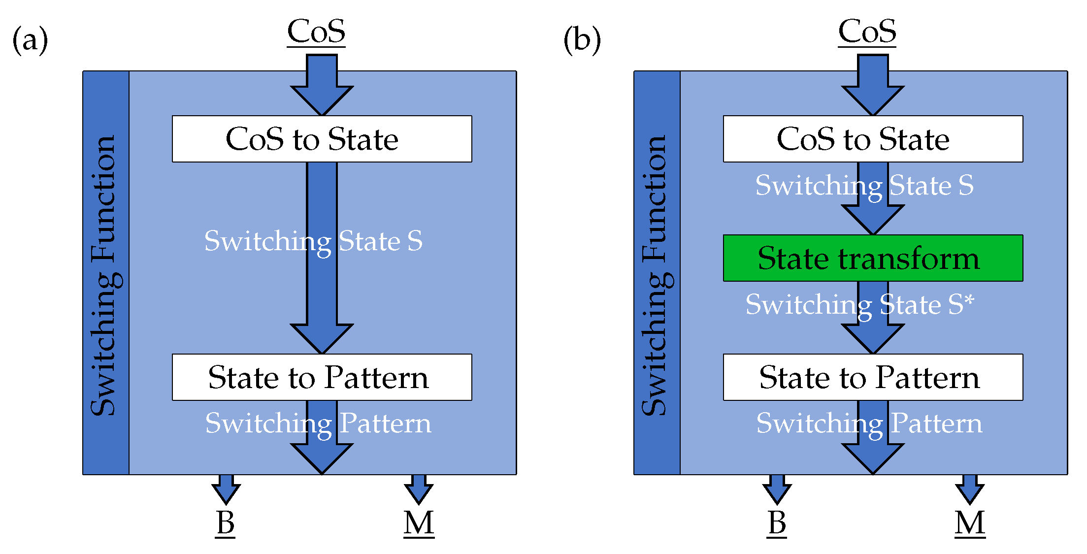
To address these shortcomings and meet more demanding control requirements, the modularisation of the lookup table concept is very effective. Here, more flexibility can be gained if a reoccurring network structure can be identified. This network structure is referred to as a submodule (SM) and is particularly associated with the class of cascaded MLIs [7,13]. Due to the identical structures, switching tables only need to be created for the switches of a single SM. Since the number of switches within an SM is only a fraction of those of an entire phase string, the size of the lookup table is massively reduced by exploiting redundant information. The SMs can be operated with the same control scheme by choosing a suitable switching table for every SM based on the intended cell’s function. The intended function of an SM’s cell demanded by the Inverter Control is referred to as the Cell operating State (CoS). A valid set of switching positions for all switches within one SM in these lookup tables is referred to as a Switching Pattern (SP). The task of a Switching Function is to assign an SP to each SM based on a Switching State (S) developed from the CoS that is input to the Switching Function (cf. Figure 3a). Since the hardware is identical with all SMs, expanding the circuit and the control by simply connecting additional SMs is easy [15].
The modular approach works efficiently for cascaded MLIs such as Cascaded H-Bridge (CHB) [8], Cascaded half Bridge (ChalfB) [7], MARX [36], Modular Multilevel Battery (M2B) [17] and Modular Multilevel Series/Parallel Converter (MMSPC) [13]. Here, the functional role of a SM’s cell can directly be applied to a SP via unique links between CoS and S and S and SP. However, a challenge for the PECIN MLI is that the assignment of S to SP is not unique. As the PECIN structure is very compactly designed, it offers much functionality with a very low number of semiconductor switches and traces on the printed circuit board. For this reason, SPs are used for more than one functionality and the resulting function of a switch depends on the switching positions of the surrounding switches. In order to assign a CoS to an SP, a state transformation from Switching State (S) to an abstracted Switching State (S*) must first be performed. S* must be selected in such a way that there is again a unique assignment from S* to SP (cf. Figure 3b)). Therefore, a more sophisticated Switching Function for the PECIN MLI is needed.

3.3. PECIN Switching Function

In Section 3.3.1, Section 3.3.2, Section 3.3.3, Section 3.3.4, Section 3.3.5, Section 3.3.6 and Section 3.3.7, the Switching Function for the PECIN MLI is developed in detail. They include an in depth analysis of the function of the PECIN topology and the underlying principles. In Section 3.3.1, input variables to the Switching Function are presented and the functional scope of the PECIN topology to an application is explained. Section 3.3.1, Section 3.3.2, Section 3.3.3, Section 3.3.4, Section 3.3.5, Section 3.3.6 and Section 3.3.7 explain in detail the process from application-based functional tasks for every cell to a SP for the phase strand as output of the Switching Function. The deliberations result in an advanced Switching Function operable on a Field Programmable Gate Array (FPGA), presented in Section 4. According to the input requirements in the CoS, it delivers a valid control signal for every switching device in the PECIN MLI, ensuring the intended and safe functionality of every single cell.

3.3.1. Inputs of the Switching Function

In order to be able to trigger a defined operating point of the inverter from the outside, input variables to the Switching Function must be provided. The operating point is defined by the application and by the BMS. The application asks for the desired voltage to be set. At the same time, the BMS monitors the energy storage limitations and a safe and optimised operation and executes advanced battery-management strategies [13,16,18,19,20,21,22]. To be able to implement these strategies with the help of the PECIN topology, it must be possible to transfer particular tasks to individual cells by electrically interconnecting these cells through SPs in such a way that the desired function, e.g., charge balancing, is implemented. Therefore, the Switching Function that implements the SPs must provide abstract inputs compatible with the BMS and voltage demand, providing sufficient scope for optimising battery operation via upstream single-cell BMS, and allow targeted action on the operation of specific battery cells. The input parameters focus on a full description of the cell’s functionality, while the switches are managed by the Switching Function. As a result, the following input parameters were identified as the Cell operating State (CoS).
It is important to note that a cell can only perform one function at a time. Therefore, the SMs are assigned to different functional subsets with ascending priority.

Subset 1: Which Cells Can Contribute?

First, the inverter control must be told which subset of the total number of cells is operational to supply the load. It takes into account that there are cells that must not be operated. The reasons why cells must not be operated are manifold. On the one hand, they can be severe safety reasons. For example, an upstream monitoring function has detected a defect in a cell [23] or that the State-of-Charge (SOC) of a cell may be too low for further discharging or too high for further charging. On the other hand, there could be requirements from the operating strategy, e.g., a balancing strategy or a diagnostic function that isolates a specific cell for further diagnostic procedures [26]. In order to be able to integrate cells into a valid load path, the Switching Function must be told which cells may be operated and which may not. Therefore, an upstream BMS must provide a vector ’cell is operable (IO)’ with one Boolean entry per cell. The entry indicates whether the cell is ready for use (logical 1) and may carry current or not (logical 0). A logical 0 uncompromisingly removes the cell from the load path.

Subset 2: Of Those That Can, Which Cells Must Contribute?

With the remaining cells, the operation of the MLI can be designed. First of all, the main task of the MLI, the setting of the desired voltage, must be ensured. After the safety issues, this is the most crucial aspect, since it is necessary to achieve the desired functionality of the connected load. Therefore, a certain number of cells must be connected in series to achieve the needed output voltage. A vector ‘Cell generates a new Voltage Level (makeLvL)’ is passed to the Switching Function to indicate these cells. It contains one entry per cell, a logical 1 if the corresponding cell adds another voltage level to the output voltage and a logical 0 if the cell must not. Via this vector, the BMS can directly instruct the inverter which specific cells contribute to the voltage generation. This setting lever could be used, e.g., to optimise charge-balancing procedures according to state-of-the-art balancing methods e.g., presented in the literature [13,16,18,19,20,21,22].

Subset 3: How Should the Cells Contribute?

The PECIN topology is a bidirectional inverter that can directly generate positive and negative output voltage values. Furthermore, with the PECIN topology, not only one polarity can be defined for the entire phase string output, but each cell can be assigned to an individual polarity for its voltage contribution to the phase string voltage independent of the polarity of the previous or subsequent cell. The definition of individual cell polarity allows to use individual cell voltages additive or subtractive to form the output voltage. The control uses this ability to increase the number of voltage levels given a number of voltage sources in asymmetric MLIs or perform a faster balancing by connecting individual cell pairs with reversed polarity [33].
A vector ’Sign of the Cell Voltage (VZ)’ with a Boolean entry for every cell, representing the sign of its voltage contribution, has to be provided to the Inverter Control. The vector entry is logical 1 for a positive and logical 0 for a negative voltage contribution. Setting every entry of VZ to the sign of the desired output voltage of the inverter makes it possible to switch to a standard operation where only additive voltage contributions are used.

Subset 4: What Happens to the Cells That Are Not Needed?

For most MLIs, the remaining cells are tied to an idle state since they are not used to operate the load. The PECIN MLI additionally offers the possibility to use the remaining cells in parallel to relieve active cells and decrease the internal resistance of the battery system [32]. A vector ‘Allow Cell in parallel Operation (allPar)’ must be specified. It contains a Boolean entry for every cell that specifies whether cells may be used in parallel operation with a neighbouring cell (logical 1) or whether the cell may only be used in serial operation (logical 0). An entry logical 0 means that the cell is separated from the load path by the SM if it is not specified makeLvL. In this case, the SM’s electrical circuitry has to bypass the cell and to open a new current path to maintain a continuous load path. Therefore, a cell can be excluded from parallel connection with other cells and forced into an idle state without interrupting overall MLI operation. The possibility of preventing parallel connection could be helpful to the control if, for example, there is a risk of equalisation currents with subsequent cells due to excessive SoC differences [32]. Furthermore, cells in idle mode serve as backup for active cells and can be used to balance the charge in the battery system in a targeted manner [15,16].

3.3.2. Declaration of the Switching State S

From the input information provided by the CoS, the function the cell assumes in the network can be derived. This function can be expressed compactly in a Switching State (S). Although the definition of S is used in the following for the PECIN topology, it is general for MLIs. In general, there are five essential functions of a cell in an MLI and the PECIN MLI is designed to offer all of them [32]. Cells can add a positive (state 1, ‘+’) or a negative (state 2, ‘−’) voltage contribution to the inverter’s output voltage in the active state. Cells that are not contributing have to be switched in parallel (state 3, ‘=’) to other contributing cells or must be bypassed (state 0, ‘0’) to keep the load path operable. The states 0–2 are distinguishable via the following definition given the previously defined input parameters.
MSB n = IO n makeLvL n VZ n ¯
LSB n = IO n makeLvL n VZ n
S n = MSB n · 2 1 + LSB n · 2 0
where n = 1 indicates the first SM of the phase, SMn is the current SM under consideration, N is the total number of SMs present in the phase string and SMN is the last SM in the phase string. The states of successive SMs can be combined into a vector S = [S1, …, Sn, …, SN]. For a purely serial operation of the PECIN topology, the states 0–2 are sufficient. A definition of state 3 for parallel cells cannot be achieved directly because parallel connections depend on surrounding cell states, as they need a cell with which they can be connected in parallel. As a design decision, it is postulated that a parallel-connected cell Zn must be preceded by a cell Zn−1 in active ‘+/−’ or parallel state ‘=’ (Sn−1∈{1, 2, 3}). Therefore, the following directed pathfinding Algorithm 1 with serial iteration from SM1 to SMN can determine SMs that fulfil these prerequisites.
Algorithm 1 Finalisation of the cell states
1:
CP = false(N,1);
2:
ParPos = false(N,1);
3:
iterPar = false;
4:
for n = 1:N
5:
leading active cells
6:
     if ∼IO(n) | | ∼allPar(n)
7:
          iterParPos = false;
8:
     end
9:
     if IO(n) && makeLvL(n) && allPar(n)
10:
          iterParPos = true;
11:
     end
12:
     ParPos(n) = iterParPos;
13:
finalisation state declaration
14:
     CP(n) = ∼makeLvL(n) && ParPos(n);
15:
     if IO(n) && ∼makeLvL(n) && CP(n)
16:
          state(n) = 3;
17:
     end
18:
end
It is important to note that the CoS has only Boolean entries. Therefore the value range for inputs is limited and both possibilities, logical 0 and logical 1, are valid for IO, makeLvL, VZ and allPar. Therefore, any input to the Switching Function will result in a valid output. Furthermore, conversion of inputs to states is only possible in a fixed set of known states 0–3. Therefore, inputs always lead to valid state sequences.

3.3.3. General Switching Patterns of the PECIN MLI

As Switching State (S) describes the abstract functional requirements of the application for every cell, the Switching Pattern (SP) represents the possibilities for reconfiguration offered by the design of the topology. While S can initially be defined as a topology-independent function of a cell in the inverter, SP embodies the topology’s functional spectrum and reconfiguration capabilities. There are different possibilities to create a SM for the PECIN topology. Therefore, the SP depends on the design of the SM, as it assigns the switches of the phase string to a specific SM. For this reason, a specific PECIN SM needs to be postulated to design the inverter’s control. First, a viewing direction from terminal N to terminal L is selected. Then, it is chosen that the previous network out of two single and two BtB MOSFETs and their connections are assigned to the following cell. This assumption leaves two switches at the highest level, which cannot be assigned to any cell if SMs are constructed equally (cf. Figure 1 and Figure 4).
For this reason, these switches form a separate unit, the Termination Unit (TU) (cf. [32]). Thereby, the PECIN MLI has four switches per SM and thus sixteen SPs, of which six SPs are of practical relevance (Figure 4) [32]. The idle state is a particular case. A single SM switched to SP6 interrupts the entire load path. For this reason, an SM can never be switched to idle in an operating inverter. However, SP6 and TUSP3 are important SPs for a switched-off inverter with high impedance output. The intended functionality of SP6 and TUSP3 can thus be mapped via an overall ‘off’-state for the entire MLI by overwriting the Switching Function’s output by logical 0. As no additional dependencies need to be considered, it is easier to integrate a general ‘off’-state and assign SP6 and TUSP3 outside the Switching Function. Therefore, the ‘off’-state is neglected in the design of the Switching Function but needs to be integrated subsequently.

3.3.4. State Transformation and Switching State S*

The aim is to achieve an output of the Switching Function that reflects the overall function of the phase string as an energetically optimal SP for the entire phase string based on the given CoS. Therefore, a matching of S and the topology-dependent SP has to be carried out to operate the inverter. In this context, the interactions between successive SMs must be examined. First, the interaction of two successive SMs is studied before the construction of an overall phase string by converting Switching State Switching State (S) into  abstracted Switching State (S*) is presented.
The quadripole of the electrical switch network Cn is connected to the input side of SMn. It can connect each input terminal {kzpn−1, kznn−1} to each output terminal {kzpn, kznn} of SMn by operating appropriate switching elements (cf. Figure 4). Cell Zn is directly connected to SMn’s output terminals {kzpn, kznn}, with its electrodes directly accessible from outside. As illustrated in Figure 5, a current can enter the quadripole of SMn at terminal kzpn−1 or terminal kznn−1. Furthermore, terminal kznn or terminal kzpn can be used to exit the quadripole. If SMn is entered, the SPn of the switching network Cn and the SPn+1 of the switching network Cn+1 determine which terminals are used and how the cell Zn is incorporated into the load path. However, given SPn the electrical connection of Zn is determined by SPn+1, as SPn+1 can allow or block the flow of current through {kzpn, kznn} of SMn. Here, the circuit Cn+1 of SMn+1 is likewise able to freely connect {kzpn, kznn} to {kzpn+1, kznn+1} of SMn+1. So there is no danger of the load path running into a dead end. Thus, for the control of SMn, only SPn is relevant if Sn is communicated to and taken into account by SMn+1. If SMn+1 respects Sn, the path through SMn can be defined by the parameters SPn and Sn alone, without the knowledge of the control in SMn+1. As a result, SPn and Sn are the parameters for the load path design in SMn and cell Zn and circuit Cn are considered as two separate quadripoles for the control (cf. Figure 5).
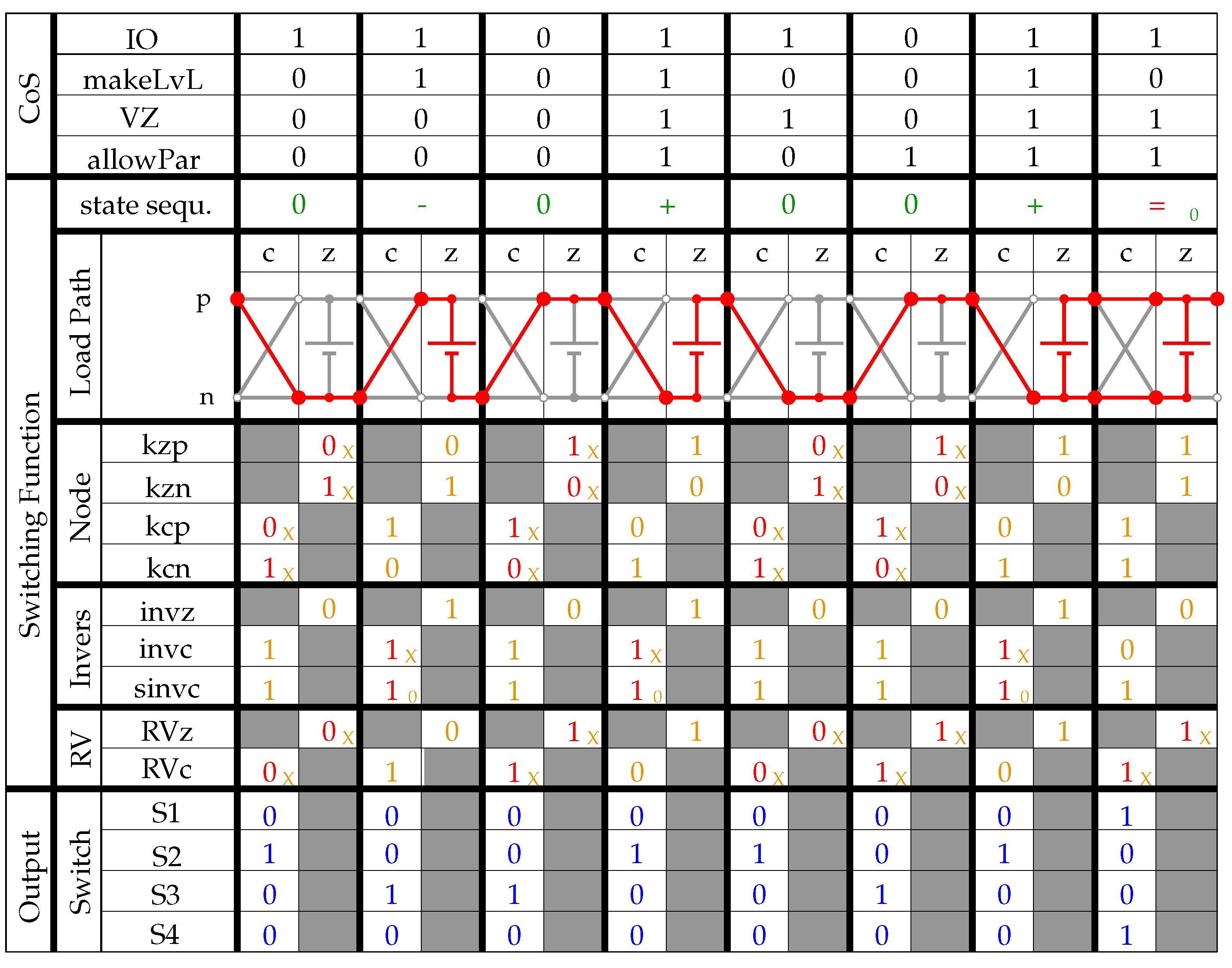
If a number of these SMs are connected in series, the model in Figure 6 has proven itself to design the control of an entire phase arm. It represents the structure of the PECIN topology by nodes and trajectories. An optimal load path can be elaborated based on the model structure and a set of rules. Through marking-involved nodes and trajectories, the load path in the network can be described.
In the model, only the output terminals of the quadripoles are considered as nodes, as they are identical to the input terminals of the following quadripole. For this reason, there are four nodes per SM, two for the cell Zn (kzpn and kznn) and two for switching network Cn (kcpn and kcnn) (cf. Figure 6). If a node is in the load path, it is marked with logical 1; otherwise, it is marked with logical 0. In addition, the trajectories between the nodes are described with a variable called the Routing Vector (RV). The RV is logical 1 if the current path changes from a negative to a positive or from a positive to a positive node and logical 0 if the path changes from a positive to a negative or a negative to a negative node. The RV contains two entries per SM, as the cell Z (Cell Routing Vector (RVz)) and circuit C (Circuit Routing Vector (RVc)) of the SM are also considered separately. The RV fully describes the load path if a starting point is given. Changes in polarity with successive RVs are of interest to the control. A transition from a positive to a negative node or a negative to a positive node is referred to as inversion. As cell and switching networks both can initiate an inversion, two variables are included. ’invc’ is logical 1 if the electrical switching network of the SM forces an inversion and ’invz’ is logical 1 if the cell forces an inversion. It is interesting to note that an inversion of a cell indicates that the cell is operated and is adding a voltage contribution to the output of the inverter. Based on the given components and their functional representations, a procedure is established to fill the entries in the table, translating the input CoS into a valid load path utilising SPs. The procedure is presented in the following and divided into four parts. First, information, which can be obtained directly, is extracted from the CoS and mapped into Switching States S. This was done in Section 3.3.2 and Section 3.3.3. In Step 2 (Section 3.3.5), initial entries can be derived from the states. Dependencies of consecutive cells, however, prevent extracting all entries directly from the input signals. Therefore, in Step 3 (Section 3.3.6), the gaps have to be filled based on the original entries and the topological knowledge. Finally, in Step 4 (Section 3.3.7), the S must be demodulated into an SP to obtain a switching state for every individual switch.

3.3.5. Init Table

Since the load path is a contiguous current path, a directed construction of the load path reduces complexity. Here, in accordance with the SM construction, a view from terminal N to terminal L of the phase string is chosen. For the definition of the initial entries, it is advantageous to have cell Z and network C quadripoles available separately. In this way, information can be derived from CoS of the SMs even if the complete insertion of SMn into the phase string cannot be fully defined directly. Direct invariant entries can be developed from S, which are stated in Table 1. Entries that cannot be defined initially are marked with an ’X’.
Properties of the PECIN MLI can be exploited with the initial entries. The beauty of the chosen definition of the SM for the PECIN topology is that the switching network C is first traversed on entry of an SM and can route every input terminal {kzpn, kznn} to every output terminal {kzpn+1, kznn+1}. Therefore, if the entry into the SMn is given, the incorporations of cell Zn and sn of Cn are independently controllable from the control and function of SMn+1 (cf. Figure 6). The positive (+) and negative (−) active state can be defined based on the requirements of Cn, leaving the trajectories between {kcpn, kcnn} and {kzpn, kznn} undefined with ’invcn  =  X’. This allows one to separate the state Sn of SMn as far as possible from Sn+1. In addition, the variable ’sinvc’ is introduced. A logical 1 in sinvcn indicates that invcn is clearly defined and a logical 0 indicates that the entry is not defined at the moment. As a result, an energetically critical feature, the avoidance of the use of a BtB MOSFET, can be implemented very easily. The use of the energetically advantageous single MOSFET is prescribed by the specification that the circuit is inverted by ‘invcn = 1’ for the bypass state (0). As the cell’s polarity is fixed, the trajectory of the switching network is used to adapt connections to previous cells with ‘invcn  =  X’. If a series of bypassed SMs occurs, the first active SM following this compound has the freedom to choose from all SPs to properly connect the cell Zn according to the intended cell state Sn. This simple definition allows using a maximum of one BtB MOSFET if the cell cannot be incorporated otherwise. This guarantees minimal usage of BtB MOSFET and therefore minimum conduction losses by minimising the internal resistance of incorporated switching devices. Furthermore, Table 1 shows that the parallel state (=) defines all node states. However, the parallel state (=) can be used with a preceding positive or a negative SM, which leaves RVc and RVz initially not determinable.

3.3.6. Finalisation

Quick and straightforward initialisation provides much information by making many entries available. The missing entries result by definition from dependencies on the previous SMs. Therefore, it is possible to iterate through the circuit from the phase terminal N to the phase terminal L and resolve the missing dependencies with Algorithm 2 (cf. Figure 6 Step 3—Finalisation).
Algorithm 2 Finalisation of the switching table
1:
for n = 1:N
2:
     RVz1 = circshift(RVz,1);
3:
     RVz1(1) = RV0;
4:
     if S(n) = = 0
5:
          kcp(n) = ∼RVz1(n);
6:
          kcn(n) = RVz1(n);
7:
          kzp(n) = kcp(n);
8:
          kzn(n) = kcn(n);
9:
          RVc(n) = kcp(n);
10:
          RVz(n) = kcp(n);
11:
     elseif S(n) = = 1
12:
          invc(n) = RVz1(n);
13:
          sinvc(n) = true;
14:
     elseif S(n) = = 2
15:
          invc(n) = ∼RVz1(n);
16:
          sinvc(n) = true;
17:
     elseif S(n) = = 3
18:
          RVc(n) = RVz1(n);
19:
          RVz(n) = RVz1(n);
20:
     end
21:
end

3.3.7. Demodulation Switching State to Switching Pattern

By filling in the table, all trajectories of the load path through the topology are known. The model was designed so that the trajectories each correspond to a link in the PECIN topology (cf. Figure 5). Here, it turns out that [RVzn−1,kcpn,kcnn] forms the abstracted Switching State (S*), which provides a unique relationship to the defined SPs. Table 2 can be used as a lookup table, converting S* to SP (cf. Figure 4). From this, the activation function Equations (4)–(9) can be determined and applied to determine the switching state for every switch.
S 1 n = kcp n ( RVz n 1 ( RVz n 1 ¯ kcn n ) )
S 2 n = RVz n 1 kcp n ¯ kcn n
S 3 n = RVz n 1 ¯ kcp n kcn n ¯
S 4 n = kcn n ( RVz n 1 ¯ ( RVz n 1 kcp n ) )
TU 1 = RVz N
TU 2 = RVz N ¯

4. FPGA Parallel Solution

The preceding sections provide a basic understanding of the PECIN topology and the general pathfinding procedure. However, some aspects were presupposed to refrain from interfering with communicating the fundamental principles. The following section focuses more deeply on control dependencies between consecutive SMs and concludes with a fully optimised Switching Function operable on an FPGA.

4.1. Solving of Dependencies between Successive Cells

As previously presented, dependencies between consecutive cells are a challenge for inverter control and require additional state transformation (cf. Figure 3). Table 1 shows that these dependencies originate from the bypass state ‘0’ and the parallel state ‘=’, where the RVs are initially undefined. These dependencies are previously resolved by serial iteration. However, it would be advantageous to determine a valid load path using parallel processing. In this way, execution delay and the dependency of the execution time on the number of SMs would be minimised. In the following, the serial dependencies are isolated so that a described routing technique can equalise them, especially with implementations on digital hardware components such as FPGAs or ASICs. In the first step, the general routing function is described. The second step identifies and analyses the functions with serial dependencies more profoundly. Finally, they are abstracted to such an extent that they are solvable by the routing technique.

4.2. Resolving Dependencies and Avoiding Iteration

As has been shown, the dependencies on previous cells prevent the initial assignment of SMs in Figure 6. Since missing entries were clarified with serial iteration in Algorithm 2, it could be assumed that a cell compound Kk = [Zn, Zn+1, …, Zn+sn−1] is started with a specific trigger event Tn that occurs before or with the evaluation of Sn. Here, [SMn, SMn+1, …, SMn+sn−1] until the next trigger event Tn+sn are associated with the SM compound Kk.
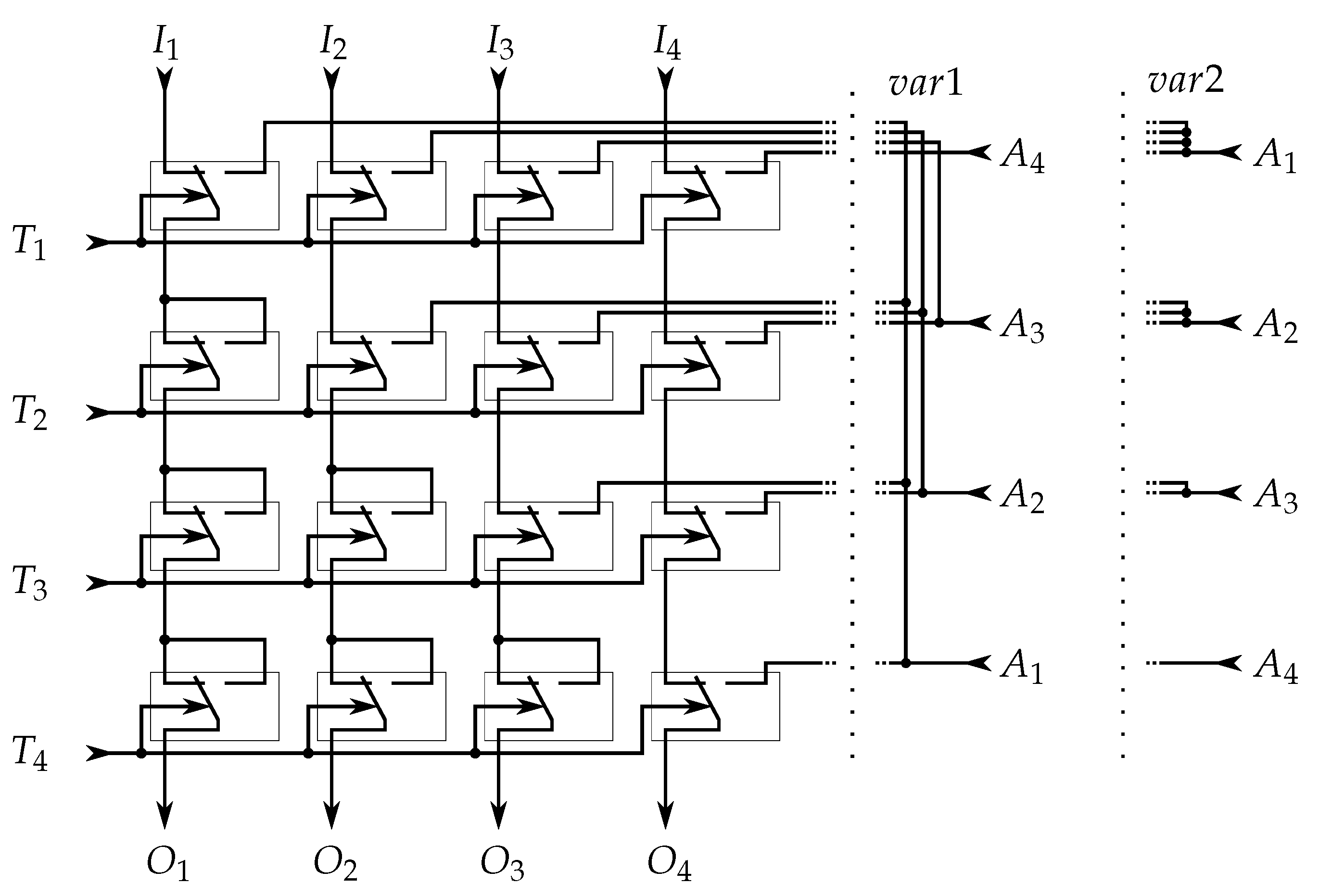
As the number of SMs in the compound Kk is variable, a direct assignment of SMs based on the trigger events Tn is possible but it requires an elaborate pre-processing and assignment process. Here, the boundaries {n,n+sn−1} of Kk must be known to distinguish Kk from Kk−1 and Kk+1. To circumvent this complexity, an overwriting procedure is used instead. Hereby, only one boundary index n is used instead of knowing both compound boundary indexes {n, n+sn−1}. Therefore, if a trigger event Tn is detected in SMn, all SMs following SMn up to SMN are assigned to the current compound Kk. To incorporate the second boundary at index {n+sn}, a subsequent trigger event Tn+s overwrites previous trigger assignments on SMn+sn to SMN. Algorithm 3 presents the procedure in pseudocode. The trigger event Tn and the insertions Sn must be present before the assignment of the compounds Kk, at least when the algorithm queries the trigger event Tn. The key is that if it is possible to detect the trigger events T = [T1, …, Tn, …, TN] based on the input parameters of the inverter and define the insertion vectors A = [A1, …, An, …, AN] in advance, the assignment can be done without serial iteration only based on routing. In this case, the output O = [O1, …, On, …, ON] can be created by routing in throughput time through the network. The routing algorithm used on the FPGA is shown in Figure 7. The described routing procedure can be used to resolve all serial dependencies in the PECIN control discussed in Section 4.3, Section 4.4, Section 4.5 and Section 4.6.
Algorithm 3 Shift and Insertion Function fct
1:
function [O] = fct(I, A, T, var)
2:
     N = length(A);
3:
     O = I;
4:
     for n = 1:N
5:
          if T(n) && var = = 1
6:
               O(n:N) = A(1:(N-n+1));
7:
          elseif T(n) && var = = 2
8:
               O(n:N) = A(n);
9:
          end
10:
     end
11:
end

4.3. Identifying Parallel Cell Compounds (ParPos)

As indicated, not all SMs that have been enabled via input ‘allowParn = 1’ for parallel connection can be connected in parallel. First, it must be ensured that SMn+1 has another SMn in active ‘+/−’ or parallel ‘=’ state to which it can be connected in parallel.
As a design variant, it is chosen that an SM or a group of SMs in a parallel state can only occur after a leading active SM in state ‘+’ or ‘−’. Therefore, no additional algorithm swaps leading parallel SMs with a subsequent active SM and an additional function must ensure that these leading parallel SMs are set to bypass state ‘0’. Therefore the intended state sequence […, 0, =, =, +, …] is not shifted to […, 0, +, =, =, …] but must be purged to sequence […, 0, 0, 0, +, …]. This circumstance is also the case if operable SMs (IO = 1) are enclosed by SMs that must not be operated (IO = 0), but for the operable SMs, no ‘makeLvL’ is provided. Here, e.g., the intended state sequence […, 0, =, =, 0, …] must be purged to sequence […, 0, 0, 0, 0, …]. Another case is given if not all SMs which are declared to be in the parallel state are preceded by an active SM. For example the intended state sequence […, 0, =, +, =, …] must be purged to sequence […, 0, 0, +, =, …]. Therefore, a preceding active SM must be identified to determine whether the following SM or a group of following SMs can be operated in parallel state ‘=’. The algorithm must identify sets of SMs that belong to these preceding cells and determine whether these sets are allowed in parallel state ‘=’. As a definition, the NFA Figure 8a describes state sequences that are switched in parallel while the NFA Figure 8b identifies state sequences that must not be. Leading active cells were previously found via serial iteration. However, a valid state sequences Pp according to NFA Figure 8a,b can be identified with the routing method described in Section 4.2. Algorithm 4 lines 4–5 identifies these sequences Pp and classifies the SMs to ensure the described behaviour.

4.4. Identification of the Area of Influence of a Sign (LvLDir)

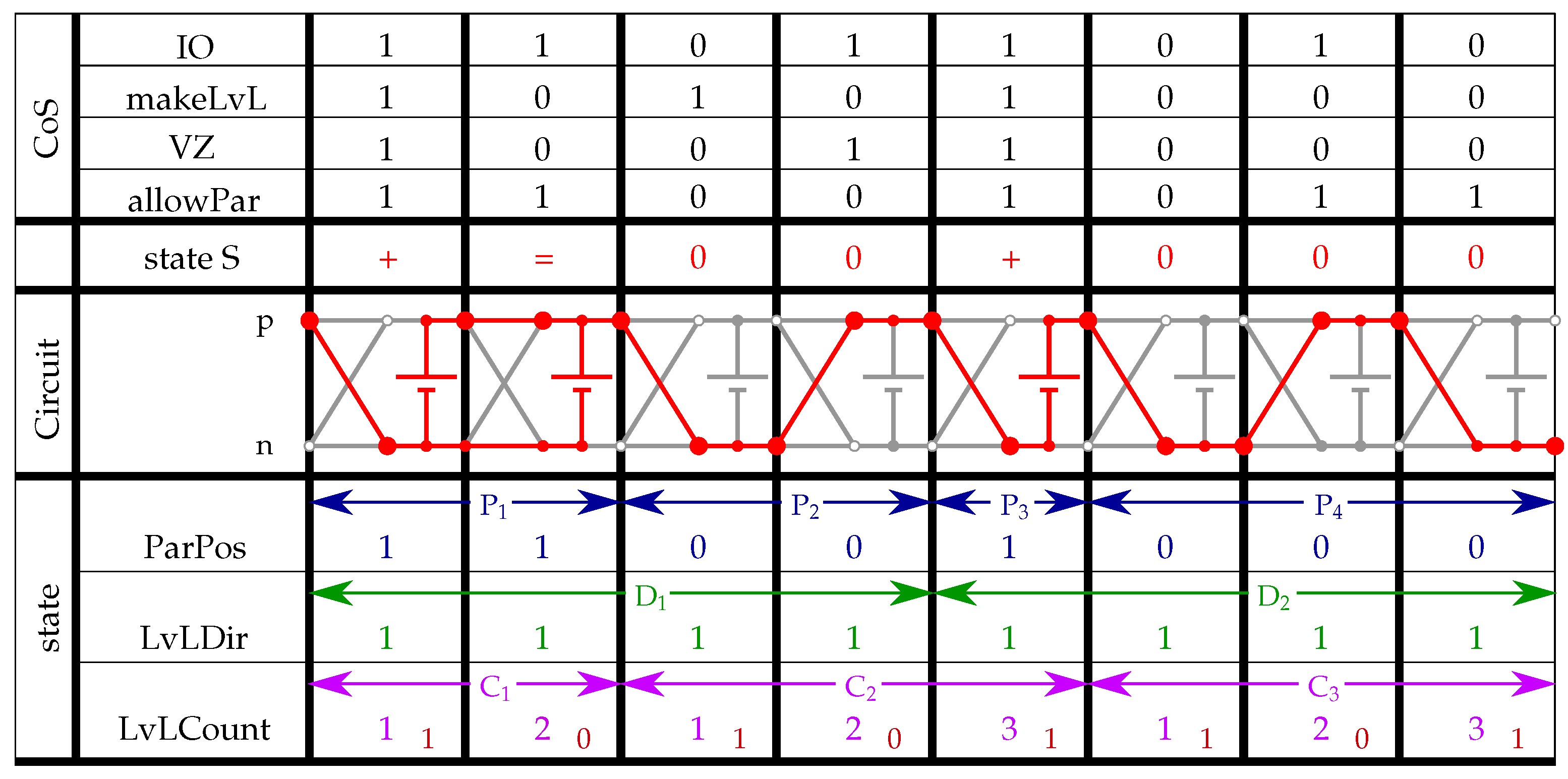
The sign of a level in the PECIN MLI is defined by the cells in active state ‘+/−’. With the definition that an SM in state parallel ‘=’ can only occur after an SM in state active ‘+/−’, the active SM is in the first position in the set Dd, in element Dd,1. A set of parallel SMs is characterised by having exactly one SM in active state ’+/−’. Each subsequent active SM [Dd+1,1, Dd+2,1, …] thus opens a new set of parallel SMs [Dd+1, Dd+2, …]. Therefore, the polarity of the leading active SM Dd,1 defines the polarity of the overall parallel compound Dd and a set of parallel SMs is linked to the voltage level l. As the state ‘=’ is polarity-independent, matching the SP3 to an SM in the parallel state ‘=’ is unique. On the other hand, the polarity of the active SM Dd,1 in the parallel network Dd is not indicated by the following SMs in parallel state ‘=’ to the first SM that is not in parallel state ‘=’. Therefore, the polarity has to be shared through the network of parallel SMs via an additional variable ’LvLDir’. Knowing the polarity of the preceding active SM is important as the next subsequent SM in state ‘+/−’ or ’0’ has to properly adapt to connect to the preceding network, to not deteriorate the intended function of the previous cell compound Dd−1 (cf. Figure 5). An example is given in Figure 9 (with Z2, Z3 and Z4) and the state sequence [+, =, 0, 0, …]. For the bypass state ’0’ of Z3, Z4 has to be in SP2 or SP4 to respect the functionality of Z3 independently of the state of Z4. A valid state sequence Dd representing a voltage level l is defined with Figure 8c.
In Algorithm 4, lines 28–32 identify these sequences and assign the polarity of the leading active SM to the SMs contained.

4.5. Identification of Cells in Bypass (LvLCount)

Bypassed SMs pose another challenge, especially when several bypassed SMs follow each other. Due to the definition that single MOSFETs are used for the bypass state ‘0’ with ‘invcn = 1’, the RVs of successive SMs in state bypass ‘0’ alternate (cf. Figure 6). Therefore, after a network of b bypassed SMs, it is not evident which output node {kzpn+b−1, kznn+b−1} the following SMn+b must connect to to achieve a proper cell functionality of Zn−1.
Algorithm 4 PECIN MLI Switching Function
1:
function [S1,S2,S3,S4,Ext1,Ext2]  =  switchFct(IO,makeLvL,VZ,allPar)
2:
     N = length(makeLvL);
3:
Identify parallel SMs
4:
     TrigParPos = ∼IO | ∼allPar | IO & makeLvL & allPar;
5:
     ParPos = fct(false(N,1), IO & makeLvL & allPar, TrigParPos, 2);
6:
 
7:
Identify leading Prebypass Cells
8:
     PBC = fct(true(N,1), false(N,1), makeLvL & IO, 2);
9:
     PBC = circshift(PBC,1);
10:
   PBC(1) = true;
11:
 
12:
Initial Direction Vector RV0
13:
     modVZ = false(N,1);
14:
     modVZ(1:2:N) = VZ(1:2:N);
15:
     modVZ(2:2:N) = ∼VZ(2:2:N);
16:
     RV0 = any(IO & makeLvL & PBC & modVZ);
17:
 
18:
Level Count
19:
Level Count: Trigger
20:
     uCML = (∼IO | ∼makeLvL & ∼ParPos | IO & makeLvL );
21:
     uCML1 = circshift(IO & (makeLvL | ParPos),1);
22:
     TrigCount = uCML1 & uCML;
23:
Level Count: Insertion
24:
     Count0 = mod([1:N]’,2);
25:
Level Count: Function
26:
     LvLCount = fct(Count0, Count0, TrigCount,1);
27:
 
28:
Level Direction
29:
Level Direction: Init
30:
     LvLDir0 = RV0 & true(N,1);
31:
Level Direction: Function
32:
     LvLDir = fct(LvLDir0, VZ, IO & makeLvL,2);
33:
 
34:
Create Cell State S
35:
     MSB = IO & (makeLvL & ∼VZ | ∼makeLvL & ParPos);
36:
     LSB = IO & (makeLvL & VZ | ∼makeLvL & ParPos);
37:
 
38:
Direction Vector RVz
39:
Direction Vector serial
40:
     RVserial = LSB & ∼MSB;
41:
Direction Vector parallel
42:
     RVparallel = LvLDir & LSB & MSB;
43:
Direction Vector bypass
44:
     RVbypass = xor(LvLCount,LvLDir) & ∼LSB & ∼MSB;
45:
Assemble Direction Vector
46:
     RVz = RVserial | RVparallel | RVbypass;
47:
 
48:
Finalising
49:
     RVz1 = circshift(RVz,1);
50:
     RVz1(1) = RV0;
51:
Finalising positive circuit knot
52:
     kcp = MSB | ∼(RVz1 | LSB);
53:
Finalising negative circuit knot
54:
     kcn = LSB | ∼(∼RVz1 | MSB);
55:
 
56:
Demodulation
57:
     S1 = kcp & (RVz1 | (∼RVz1 & kcn));
58:
     S2 = RVz1 & ∼kcp & kcn;
59:
     S3 = ∼RVz1 & kcp & ∼kcn;
60:
     S4 = kcn & (∼RVz1 | (RVz1 & kcp));
61:
     TU1 = RVz(N);
62:
     TU2 = ∼RVz(N);
Algorithm 2 uses serial iteration to guarantee proper connection of Zn−1 as it can chose SPn+b freely (cf. ‘invcn+b = X’). However, to solve the problem in a parallel fashion, a central aspect is to determine the continuous compounds of bypassed SMs in the phase string. Therefore, the SMs in the phase string are assigned to compounds [C1, …, Cc, …, CC]. As SPn+b can be freely chosen from {SP1, SP2, SP4, SP5}, the choice of the SP (either SP1 or SP2) of the bypassed SMs [SMn, …, SMn+b−1] is dependent on the number b of bypassed SMs and RVn−1 of SMn−1, which is in active ‘+/−’ or parallel ‘=’ state. Here, counting is a vital aspect of solving this challenge, even if counting is, in general, a serial method. Regarding a compound Cc, the counting of its elements can be simplified, if the leading SMs in Cc are the b bypassed SMs by definition, if bypass SMs are present. In this case, the count always starts with a count value of one. Given the polarity of SMn−1, it is not the assigned number of the bypassed SMn that is important for determining the polarity of RVn+b−1, but whether the bypassed SM is an even or an odd cell number in the compound Cc. For the determination of the RVs, only the numbering of the leading SMs in state bypass ’0’ is relevant. By definition, the SMn+b is in active state ‘+/−’. In addition, SMn+b can be followed by a compound of SMs in parallel state. Therefore, Cc is defined as [SMn, …, SMn+a+b−1]. Cc+1 starts with the next bypassed SMs or an SM in active state ‘+/−’. The numbering of SMn to SMn+a+b−1 is not necessary but is done to easily create and fill a vector with fixed length N for the phase string. With a count value always starting with one, the problem can be simplified considerably by having one Boolean LvLCount vector containing only logical 0 for even cells and logical 1 for odd cells (cf. Figure 9). To complete the connection of SMn+b, SMn must be identified. In accordance with the given definition, a valid state sequence Cc is applied in accordance with Figure 8c.
In Algorithm 4, lines 18–26 solve state dependencies of bypassed SM compounds. As an output, they deliver LvLCount, the concatenated counting vector [C1, …, Cc, …, CC] (cf. Figure 9). Then two cases are distinguishable, positive and negative node connectivity of SMn (kzpn−1, kznn−1). This circumstance is solved in Algorithm 4 line 44 with the help of LvLDir.

4.6. Determination of the Initial RV (PreBypass)

A starting point must be defined for the construction of the load path. In the examples presented in Figure 6 and Figure 9, the initial Routing Vector RV0 = 1 was tacitly given by starting with kcp0 = 1 and kcn0 = 0. However, an optimal value for the RV0 can only be set directly if the first SM in the string is in state ‘+’ or ‘−’. If the phase string starts with a minimum of one bypassed SM, RV0 can be chosen freely between logical 1 or logical 0 while Algorithm 4 always generates a valid load path.
In the simplest case, RV0 is therefore fixed or, better, given by the sign of the desired inverter output voltage. This load path respects the given CoS, but may not be energetically optimal as it may use a BtB MOSFET even if it is not necessary. Especially with SM compounds bordering phase terminal N or L, an optimal path that does not contain any BtB MOSFET can always be found with the PECIN topology. To avoid the usage of BtB MOSFETs, a further evaluation of the leading e bypassed cells has to take place via an additional Prebypass function.
For the Prebypass function, the procedure is similar to the general bypassing. However, contrary to the previous definition, the polarity of the network depends on RVe+1 of the first SM after the network of e bypassed SMs and not at the polarity of SM1 in front of the e bypassed SMs. By definition, SMe+1 is in active ‘+/−’ state. First, the compound B = [SM1, …, SMe] must be identified. Unfortunately, ParPos does not reveal the needed information to achieve Prebypass, as ParPos does not reveal the position of SMe+1 without further processing. However, the position and the polarity of SMe+1 is crucial here. Therefore, the vector PBC is built within Algorithm 4 lines 8–10, according to [PBS1 …PBSe] = true and [PBSe+1 …PBSN] = false. After identifying the first active SM, the iteration direction would therefore run in reverse, to the previously used definition, from terminal L to N.
Depending on RVe+1 and the number e of preceding bypassed SMs, it is then possible to optimally define RV0. For the calculation, a distinction can be made based on the sign VZe+1 of the voltage contribution of SMe+1 (cf. Equation (13)). Two calculations are carried out in parallel. One that assumes an RVe+1 = true and one that assumes an RVe+1 = false (cf. Equations (10) and (11)). As with LvLCount, the vector Ct contains the least significant bit of the count value [1, 2, …N] and indicates an even or an odd SM number.
RV 0 p = n = 1 N I O n m a k e L v L n P B C n 1 V Z n C t n
RV 0 n = n = 1 N I O n m a k e L v L n P B C n 1 V Z n ¯ C t n ¯
Ct = [ t r u e f a l s e t r u e f a l s e ]
RV 0 = RV 0 p RV 0 n
On closer inspection of the equations, every second entry is associated with a logical 0 entry of the Ct vector (cf. Equation (12)).
From this follows a reduced procedure presented in Algorithm 4 lines 12–16. For the first SM, initial values {kzp0,kzn0} must be defined via the calculated RV0 with kzp0 = RV0 and kzn0 = ∼RV0.
The paper contains a digital Supplementary Materials with a Matlab/Simulink model for the Switching Function presented in Section 3 and an implementation of Algorithm 4 in Matlab code and Xilinx Vitis Model Composer for Matlab/Simulink.

5. Practical Validation

A test stand was built to evaluate the PECIN MLI in [32] (cf. Figure 10). The test stand includes a measurement and control system, the newly developed PECIN board, battery cells and a load to operate the inverter.
The PECIN MLI was designed on a circuit board with N = 8 SMs. The inverter board is connected to Samsung INR18650-25R battery cells with a nominal capacity of 2500 mAh (4.2 V–2.5 V, 0.2 C). The inverter thus has a nominal peak output voltage of 28.8 V with L = 17 voltage levels. Enhancement mode N-channel MOSFETs of type ON Semiconductor NTMTS0D6N04CL with a nominal RDS,on of 420 µ Ω were used. The test stand is controlled via a dSpace Scalexio Processing Unit. All aspects presented in this publication regarding the Switching Function are merged into Algorithm 4. The algorithm is designed with basic logic operations and adopted on a DS6602 FPGA Base Board with a Xilinx Kintex UltraScale+ KU15P FPGA. The FPGA was programmed using the dSpace toolchain and the Vivado Design Suite from Xilinx in Matlab Simulink. The main load for the experiments is a stator of an SEW Eurodrive DRS71M2 asynchronous machine. Measurements were taken with a Teledyne LeCroy Wavesurver 3024 digital oscilloscope.
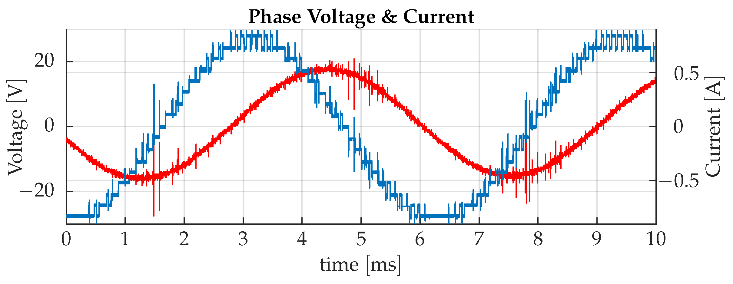
Ref. [32] presents measurements and an efficiency analysis carried out using Algorithm 4 for PECIN MLI control. In addition, Figure 11 presents measurements with a 20 kHz setpoint update of the Space Vector Modulation presented in [37] to show the real-time capability with higher switching frequencies. A static dead time of 800 ns is used for all switches, which was determined empirically.

6. Conclusions and Outlook

Since switching device control is safety-critical and essential to MLI usability, our publication provided a structured and easy-to-use Switching Function for the novel PECIN MLI. The Switching Function abstracts the control of the inverter from the control of the switching elements through functional states that represent the individual battery cells’ contribution to the overall phase string’s task. Thus, it simplifies the control by accepting functional states derived from the application, which are easily understood and directly usable for higher-level inverter control and battery management.
First, these important input parameters were identified as IO, makeLvL, VZ and allPar, with which battery management and the application get full access to inverter control by defining single-cell operation besides overall phase string functionality. Second, the methodology of the Switching Function was presented. It contained a deep analysis of how this input is converted into correct and deterministic switching commands for every switch to guarantee safe operation, correct output voltage and exact execution of the battery-management requirements. The primary benefit of the implemented and tested Switching Function is that the methodology ensures that inputs are always converted into safe and intended switching behaviour of the PECIN MLI. In doing so, inputs are monitored and, if necessary, adjusted to resolve invalid or competing input specifications into valid states. Furthermore, our Switching Function provides an energy-optimal load path through the MLI topology by avoiding the operation of BtB MOSFETs. During development, care was taken to simplify the function to achieve a minimum execution delay on the target device. As it turned out, the inverter control is fast enough to set a Switching Pattern with a setpoint update of 20 kHz.
With the Switching Function presented, we have created the basis for the most flexible operation of the PECIN topology possible to meet the researchers’ demands for testing different operating strategies and higher-level inverter control. In addition, our article provided a deeper understanding and advanced knowledge of multilevel inverter control in general. In particular, we highlighted the control of the novel PECIN topology. Combined, it will allow the scientific audience to quickly and confidently use the new topology, thereby accelerating research on this promising new inverter type.

Supplementary Materials

The following supporting information can be downloaded at: https://www.mdpi.com/article/10.3390/electronics12143130/s1, PDF-File: Readme_SimulationSwitching Function.pdf; Matlab Code: Init_SimulationSwitchingFunction.m; Matlab Code: fct.m; Simulink Model: SimulationSwitchingFunction.slx.

Author Contributions

Conceptualisation, C.T. and S.S.; methodology, C.T.; software, C.T.; validation, C.T. and S.S.; formal analysis, C.T.; investigation, C.T.; resources, C.T.; data curation, C.T.; writing—original draft preparation, C.T.; writing—review and editing, S.S.; visualisation, C.T.; supervision, C.E.; project administration, C.E.; funding acquisition, C.E. and S.S. All authors have read and agreed to the published version of the manuscript.

Funding

This research was funded by Project LernBaLanz by StmWK Bavaria and the used equipment by BMBF (grant 13FH058INO). In addition, we acknowledge support by the German Research Foundation and the Open Access Publication Fund of Technische Hochschule Ingolstadt.

Data Availability Statement

Supplementary Materials are available under the terms of the CC BY-SA: C. Terbrack (2023) Data from: Control and Implementation of the Parallel Enhanced Commutation Integrated Nested Multilevel Inverter Topology.

Acknowledgments

The authors thank Meinert Lewerenz for the valuable discussions and suggestions on the presentation of the topic. In addition, we thank A. Frey and X. Zhao for the preparation of hardware components used for the investigations.

Conflicts of Interest

The authors declare no conflict of interest.

Abbreviations

The following abbreviations are used in this manuscript:
BEVBattery Electric Vehicle
BCSBridge-Type Connected Source
BMSBattery-Management System
BtBBack-to-Back
CHBCascaded H-Bridge
ChalfBCascaded half Bridge
ClClosing (Unit)
CCSCascaded Cross-Switched
CoSCell operating State
CSCross-Switched
ECINEnhanced Commutation Integrated Nested
FPGAField Programmable Gate Array
M2BModular Multilevel Battery
MLIMultilevel Inverter
MMLCModular Multilevel Converter
MMSPCModular Multilevel Series/Parallel Converter
MOSFETMetal-Oxide-Semiconductor Field-Effect Transistor
NFANondeterministic Finite Automaton
NLCNearest Level Control
OCVOpen-Circuit Voltage
PCBPrinted Circuit Board
PECINParallel Enhanced Commutation Integrated Nested
PWMPulse Width Modulation
RVRouting Vector
SMSubmodule
SOCState-of-Charge
SPSwitching Pattern
SSwitching State
S*abstracted Switching State
SVCSpace Vector Control
THD        Total Harmonic Distortion
TUTermination Unit

References

  1. Lu, L.; Han, X.; Li, J.; Hu, J.; Ouyang, M. A review on the key issues for lithium-ion battery management in electric vehicles. J. Power Sources 2013, 226, 272–288. [Google Scholar] [CrossRef]
  2. Emadi, A. Advanced Electric Drive Vehicles, 1st ed.; CRC Press: Boca Raton, FL, USA, 2014. [Google Scholar]
  3. Sang-Hoon, K. Chapter 7—pulse width modulation inverters. In Electric Motor Control; Elsevier: Amsterdam, The Netherlands, 2017; pp. 265–340. [Google Scholar]
  4. Singh, G.; Garg, V.K. Thd analysis of cascaded h-bridge multi-level inverter. In Proceedings of the 2017 4th International Conference on Signal Processing, Computing and Control (ISPCC), Solan, India, 21–23 September 2017; pp. 229–234. [Google Scholar] [CrossRef]
  5. Marquardt, R. Modular Multilevel Converter: An universal concept for HVDC-Networks and extended DC-Bus-applications. In Proceedings of the 2010 International Power Electronics Conference—ECCE ASIA, Sapporo, Japan, 21–24 June 2010; pp. 502–507. [Google Scholar] [CrossRef]
  6. Nami, A.; Liang, J.; Dijkhuizen, F.; Demetriades, G.D. Modular Multilevel Converters for HVDC Applications: Review on Converter Cells and Functionalities. IEEE Trans. Power Electron. 2015, 30, 18–36. [Google Scholar] [CrossRef]
  7. Lesnicar, A.; Marquardt, R. An innovative modular multilevel converter topology suitable for a wide power range. In Proceedings of the 2003 IEEE Bologna Power Tech Conference Proceedings, Bologna, Italy, 23–26 June 2003; Volume 3, p. 6. [Google Scholar] [CrossRef]
  8. Baker, R.H.; Bannister, L.H. Electric Power Converter. U.S. Patent 3867643, 18 February 1975. [Google Scholar]
  9. Quraan, M.; Tricoli, P.; D’Arco, S.; Piegari, L. Efficiency assessment of modular multilevel converters for battery electric vehicles. IEEE Trans. Power Electron. 2017, 32, 2041–2051. [Google Scholar] [CrossRef]
  10. Korte, C.; Specht, E.; Hiller, M.; Goetz, S. Efficiency evaluation of mmspc/chb topologies for automotive applications. In Proceedings of the 2017 IEEE 12th International Conference on Power Electronics and Drive Systems (PEDS), Toulouse, France, 9–12 July 2019; pp. 324–330. [Google Scholar] [CrossRef]
  11. Chang, F.; Ilina, O.; Lienkamp, M.; Voss, L. Improving the Overall Efficiency of Automotive Inverters Using a Multilevel Converter Composed of Low Voltage Si mosfets. IEEE Trans. Power Electron. 2019, 34, 3586–3602. [Google Scholar] [CrossRef]
  12. Kersten, A.; Kuder, M.; Grunditz, E.; Geng, Z.; Wikner, E.; Thiringer, T.; Weyh, T.; Eckerle, R. Inverter and battery drive cycle efficiency comparisons of chb and mmsp traction inverters for electric vehicles. In Proceedings of the 2019 21st European Conference on Power Electronics and Applications (EPE), Genova, Italy, 3–5 September 2019; pp. 1–12. [Google Scholar] [CrossRef]
  13. Goetz, S.M.; Peterchev, A.V.; Weyh, T. Modular multilevel converter with series and parallel module connectivity: Topology and control. IEEE Trans. Power Electron. 2015, 30, 203–215. [Google Scholar] [CrossRef]
  14. Kangarlu, M.F.; Babaei, E.; Sabahi, M. Cascaded crossswitched multilevel inverter in symmetric and asymmetric conditions. IET Power Electron. 2013, 6, 1041–1050. [Google Scholar] [CrossRef]
  15. Komsiyska, L.; Buchberger, T.; Diehl, S.; Ehrensberger, M.; Hanzl, C.; Hartmann, C.; Hölzle, M.; Kleiner, J.; Lewerenz, M.; Liebhart, B.; et al. Critical Review of Intelligent Battery Systems: Challenges, Implementation and Potential for Electric Vehicles. Energies 2021, 14, 5989. [Google Scholar] [CrossRef]
  16. Goetz, S.M.; Li, Z.; Liang, X.; Zhang, C.; Lukic, S.M.; Peterchev, A.V. Control of Modular Multilevel Converter with Parallel Connectivity Application to Battery Systems. IEEE Trans. Power Electron. 2017, 32, 8381–8392. [Google Scholar] [CrossRef]
  17. Helling, F.; Glück, J.; Singer, A.; Weyh, T. Modular multilevel battery (m2b) for electric vehicles. In Proceedings of the 2016 18th European Conference on Power Electronics and Applications (EPE’16 ECCE Europe), Karlsruhe, Germany, 5–9 September 2016; pp. 1–9. [Google Scholar] [CrossRef]
  18. Babaei, E. Charge Balance Control Methods for a Class of Fundamental Frequency Modulated Asymmetric Cascaded Multilevel Inverters. J. Power Electron. 2011, 11, 811–818. [Google Scholar] [CrossRef] [Green Version]
  19. Vasiladiotis, M.; Rufer, A. Balancing control actions for cascaded H-bridge converters with integrated battery energy storage. In Proceedings of the 15th European Conference on Power Electronics and Applications (EPE), Lille, France, 2–6 September 2013; pp. 1–10. [Google Scholar] [CrossRef]
  20. Raj, N.; Jagadanand, G.; George, S. A Modified Charge Balancing Scheme for Cascaded H-Bridge Multilevel Inverter. J. Power Electron. 2016, 16, 2067–2075. [Google Scholar] [CrossRef]
  21. Mashayekh, A.; Kersten, A.; Kuder, M.; Estaller, J.; Khorasani, M.; Buberger, J.; Weyh, T. Proactive SoC Balancing Strategy for Battery Modular Multilevel Management (BM3) Converter Systems and Reconfigurable Batteries. In Proceedings of the 23rd European Conference on Power Electronics and Applications (EPE’21 ECCE Europe), Virtual, 6–10 September 2021; pp. 1–10. [Google Scholar] [CrossRef]
  22. Porras, J.S.; Ioan-Stroe, D.; Sangwongwanich, A. State-Of-Energy Balancing Control with Cascaded H-Bridge for Second-Life Batteries. In Proceedings of the IEEE Applied Power Electronics Conference and Exposition (APEC), Long Beach, CA, USA, 25–29 February 2023; pp. 571–576. [Google Scholar] [CrossRef]
  23. Schmid, M.; Gebauer, E.; Hanzl, C.; Endisch, C. Active Model-Based Fault Diagnosis in Reconfigurable Battery Systems. IEEE Trans. Power Electron. 2021, 36, 2584–2597. [Google Scholar] [CrossRef]
  24. Theiler, M.; Schneider, D.; Endisch, C. Experimental Investigation of State and Parameter Estimation within Reconfigurable Battery Systems. Batteries 2023, 9, 145. [Google Scholar] [CrossRef]
  25. Helling, F.; Glück, J.; Singer, A.; Pfisterer, H.-J.; Weyh, T. The ac battery a novel approach for integrating batteries into ac systems. Int. J. Electr. Power Energy Syst. 2019, 104, 150–158. [Google Scholar] [CrossRef]
  26. Liebhart, B.; Diehl, S.; Schmid, M.; Endisch, C.; Kennel, R. Improved Impedance Measurements for Electric Vehicles with Reconfigurable Battery Systems. In Proceedings of the 2021 IEEE 12th Energy Conversion Congress & Exposition-Asia (ECCE-Asia), Singapore, 24–27 May 2021; pp. 1736–1742. [Google Scholar] [CrossRef]
  27. Schwitzgebel, F.; Buberger, J.; Kuder, M.; Karnehm, D.; Sorokina, N.; Wiedenmann, A.; Mashayekh, A.; Eckerle, R.; Weyh, T. Multilevel Inverter based Battery System Operation using a Decentralized Controller. In Proceedings of the 2022 International Conference on Smart Energy Systems and Technologies (SEST), Eindhoven, The Netherlands, 5–7 September 2022; pp. 1–6. [Google Scholar] [CrossRef]
  28. Quraan, M.; Abu-Khaizaran, M.; Sa’ed, J.; Hashlamoun, W.; Tricoli, P. Design and control of battery charger for electric vehicles usingmodular multilevel converters. IET Power Electron. 2021, 14, 140–157. [Google Scholar] [CrossRef]
  29. Alatai, S.; Salem, M.; Ishak, D.; Bughneda, A.; Kamarol, M.; Luta, D.N. Cascaded Multi-Level Inverter for Battery Charging-Discharging using Buck-Boost Switch. In Proceedings of the 2021 IEEE Industrial Electronics and Applications Conference (IEACon), Virtual, 3–4 October 2021; pp. 108–112. [Google Scholar] [CrossRef]
  30. El-Hosainy, A.; Hamed, H.A.; Azazi, H.Z.; El-Kholy, E.E. A review of multilevel inverter topologies, control techniques and applications. In Proceedings of the 2017 19th International Middle East Power Systems Conference (MEPCON), Cairo, Egypt, 19–21 December 2017; pp. 1265–1275. [Google Scholar] [CrossRef]
  31. Venkataramanaiah, J.; Suresh, Y.; Panda, A.K. A review on symmetric, asymmetric, hybrid and single dc sources based multilevel inverter topologies. Renew. Sustain. Energy Rev. 2017, 76, 788–812. [Google Scholar] [CrossRef]
  32. Terbrack, C.; Stöttner, J.; Endisch, C. Design and Validation of the Parallel Enhanced Commutation Integrated Nested Multilevel Inverter Topology. IEEE Trans. Power Electron. 2022, 37, 15163–15174. [Google Scholar] [CrossRef]
  33. Gupta, K.K.; Jain, S. Topology for multilevel inverters to attain maximum number of levels from given DC sources. IET Power Electron. 2012, 5, 435–446. [Google Scholar] [CrossRef]
  34. Kangarlu, M.F.; Babaei, E. Cross-switched multilevel inverter: An innovative topology. IET Power Electron. 2013, 6, 642–651. [Google Scholar] [CrossRef]
  35. Kamaldeep; Kumar, J. Switch reduction and performance analysis using different modulation technique in multilevel inverter. In Proceedings of the 2016 IEEE 1st International Conference on Power Electronics, Intelligent Control and Energy Systems (ICPEICES), Delhi, India, 4–6 July 2016; pp. 1–4. [Google Scholar] [CrossRef]
  36. Rodriguez, J.; Leeb, S. A multilevel inverter topology for inductively-coupled power transfer. In Proceedings of the 18th Annual IEEE Applied Power Electronics Conference and Exposition (APEC ’03), Miami, FL, USA, 9–13 February 2003; Volume 2, pp. 1118–1126. [Google Scholar] [CrossRef]
  37. Zhang, H.; Meng, Y.; Ning, L.; Zou, Y.; Wang, X.; Wang, X. Fast and simple space vector modulation method for multilevel converters. IET Power Electron. 2020, 13, 14–22. [Google Scholar] [CrossRef]
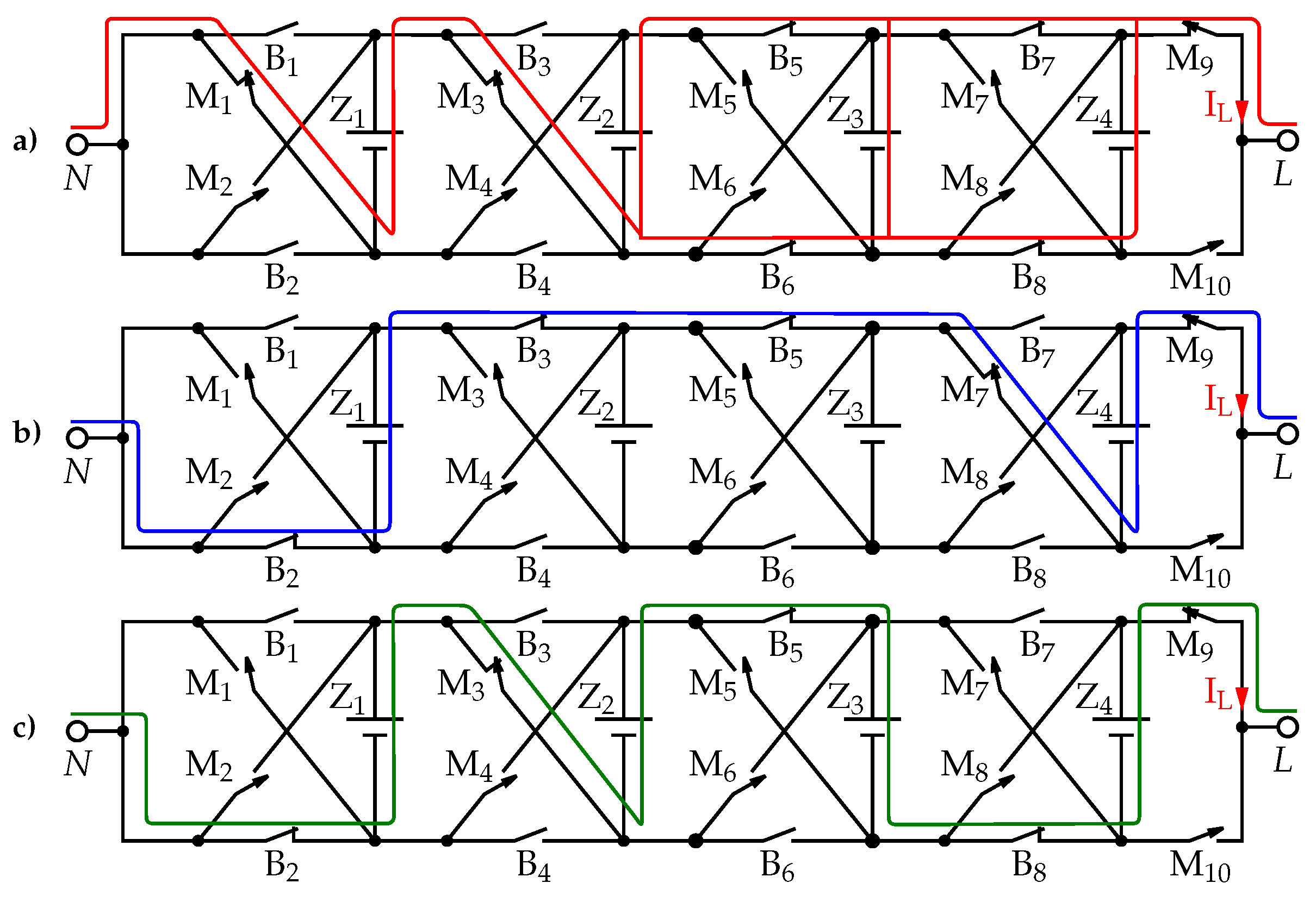
Figure 1. A 9-Level PECIN MLI with BTB MOSFETs (B 1 –B 8 ), single MOSFET (M 1 –M 10 ), battery cells (Z 1 –Z 4 ) and exemplary load paths (ac).
Electronics 12 03130 g001
Figure 2. Schematic of Inverter Control with Traction Control, Inverter Management, PECIN MLI hardware and Electrical Machine.
Electronics 12 03130 g002
Figure 3. Switching Function for cascaded multilevel inverters: (a) standard procedure with unique assignment of Cell operating State (CoS) to the Switching State (S) and (b) modified PECIN Switching Function.
Electronics 12 03130 g003
Figure 4. Valid Switching Patterns of the PECIN MLI: Submodule (SM) und Termination Unit (TU).
Electronics 12 03130 g004
Figure 5. Dependencies of the load paths through PECIN submodule SMn based on the SP of submodule SMn and SMn+1.
Electronics 12 03130 g005
Figure 6. Generation of a load path in a PECIN phase arm: Step 1—State declaration (green); Step 2—Initialisation (yellow); Step 3—Finalisation (red); Step 4—Demodulation (blue).
Electronics 12 03130 g006
Figure 7. FPGA Implementation of the shift and insertion Function fct.
Electronics 12 03130 g007
Figure 8. NFA representing valid state sequences for (a) Pp in ParPos: Cells in parallel (b) Pp in ParPos: Cells not in parallel (c) Dd in LvLDirect (d) Cc in LvLCount.
Electronics 12 03130 g008
Figure 9. Usage and Boundaries of LvLDir (green), LvLCount (purple) and ParPos (blue).
Electronics 12 03130 g009
Figure 10. PECIN test stand with PECIN demonstrator board.
Electronics 12 03130 g010
Figure 11. Achieved output voltage (blue) and current (red) with the PECIN demonstrator board and test stand in Figure 10 with a 20 kHz setpoint update.
Electronics 12 03130 g011
Table 1. Init table entries based on Switching State Sn.
kzpkznkcpkcninvzinvcsinvcRVzRVc
Bypass (0)XXXX011XX
Positive active (+)10011X010
Positive active (−)01101X001
Parallel (=)1111001XX
Table 2. Derivation of the Switching Pattern from the abstracted Switching State S*.
S*RV Z n 1 01010101
kcp n 00110011
kcn n 00001111
SP n SP6SP6SP2SP5SP4SP1SP3SP3
Disclaimer/Publisher’s Note: The statements, opinions and data contained in all publications are solely those of the individual author(s) and contributor(s) and not of MDPI and/or the editor(s). MDPI and/or the editor(s) disclaim responsibility for any injury to people or property resulting from any ideas, methods, instructions or products referred to in the content.