Abstract
It is challenging to design high-gain amplifiers near the maximum oscillation frequency (fmax) of the transistors. This paper presents a comprehensive graphical approach to maximize the gain of feedback amplifiers with maximally efficient gain (GME) conception at near-fmax frequency. The complex gain-plane and the reflection-coefficient-plane are utilized to provide clear insights into both the gain and stability states of the two-port device while boosting GME. An efficient flowchart to synthesize feedback amplifiers is given, which optimizes the GME of a two-port device while ensuring the stability. A 210 GHz power amplifier in 40 nm CMOS was designed and optimized based on the proposed approach. The feedback circuit of the transistor pushes it to become potentially unstable and boosts GME. The measured peak small-signal gain was 10.48 dB at 195.33 GHz. The measured saturation output power and large-signal gain at 210 GHz were 3.04 dBm and 7.08 dB, respectively. The presented method could facilitate terahertz amplifier design.
1. Introduction
Terahertz (THz) frequencies of 100–300 GHz have received attention in various fields, such as high-data-rate communication, imaging, and radar [,,,]. THz amplifiers are one of the most important parts in the THz transceivers for these applications. Since THz frequencies are very close to the fmax of the active devices, the available gain from the active devices declines rapidly at these frequencies. Consequently, it is challenging to design high-gain near-fmax THz amplifiers.
It has been shown that boosting the power gain of an active two-port device (A2P) to its maximum achievable gain (GMAX) using specific embedding is a promising solution to the power gain issue [,]. However, GMAX has disadvantages. GMAX is achieved only when the source and load impedances are conjugate-matched to the input and output terminals of the A2P simultaneously, which is possible only when the A2P is unconditionally stable. For a potentially unstable A2P, GMAX is not defined and provides no useful design information []. The design of the GMAX-based amplifier is thus limited in its unconditionally stable state.
The maximally efficient gain GME is another figure of merit for A2Ps []. It is defined as the power gain that maximizes the added power of the A2P. It is achieved by choosing a certain set of the source and load admittances. Advantages of GME include that it provides outstanding large-signal performances and that it is well-behaved both for stable and unstable A2Ps, which broaden the design space and bring potential for boosting the power gain beyond GMAX. These features have attracted increasing attention from designers. The GME-based designs have been successfully applied in amplifiers [,,] and oscillators [,].
Despite the excellent features of GME, the GME-based designs have not been studied comprehensively. No analytical solution has been developed yet to optimize GME. In amplifier design, it is crucial to ensure that both terminals of the amplifier are stable. The advantage of GME that it is well-behaved for the potentially unstable A2P, however, raises the risk of oscillation for a GME-based amplifier, making the design complex and difficult. An efficient and accurate design method for optimizing GME-based amplifiers is urgently needed.
In this paper, a graphical approach to optimize the GME of amplifiers is presented. The gain-plane and the reflection-coefficient-plane are employed to visualize both the gain and stability states of an A2P. The optimum position of GME on the gain-plane is determined. Embeddings are used to form a feedback circuit and create a two-dimensional movement on both planes to move the A2P to the desired position. A flowchart is developed to efficiently design the embedding that optimizes the GME of the A2P. The proposed process is capable of boosting the gain of a single NMOS transistor in a 40 nm CMOS process up to 7.68 dB at 200 GHz while ensuring the stability in both input and output terminals.
The remainder of this paper is organized as follows. Section 2 studies the gain-plane and reflection-coefficient-plane for a GME-based A2P. Section 3 derives the movement of the A2P on both planes using various embeddings. Section 4 presents the flowchart for maximizing the GME of the feedback amplifier. In Section 5, a two-stage embedded amplifier at 210 GHz is presented using the proposed approach, and the measurement results are presented. Finally, Section 6 concludes this paper.
2. Gain-Plane and Reflection-Coefficient-Plane
The maximally efficient gain GME of an A2P is given by []:
where Yij (i, j = 1, 2) is the Y-parameter of the A2P, and G11 and G22 are the real parts of Y11 and Y22, respectively. It is obtained when the load admittance YL of the A2P is set to
The source admittance YS is chosen to be the complex conjugate of the input admittance:
where Yij are the Y parameters of the A2P. Equations (2) and (3) can also be expressed in terms of Z parameters:
GME can be rewritten in terms of Rollett’s stability k and complex inverse gain λ = Y12/Y21:
where k is expressed as a function of λ and unilateral power gain U []:
where λR and λI are the real and imaginary parts of λ, respectively. Using Equation (7), GME can be rewritten in terms of λ and U:
Equations (7) and (8) describe the loci of constant-k contours and constant-GME circles on the complex λ-plane (also called the gain-plane), respectively, as shown in Figure 1a. For a given A2P, its coordinate on the gain-plane represents the gain state and is determined by its Y parameters Y12/Y21. The coordinate of a 40 nm NMOS transistor at 200 GHz is plotted in Figure 1a. Two observations are obtained from Figure 1a. The first is that for a given GME, the left intersection point of the constant-GME circle with the X-axis gives the largest k. Although the value of k cannot be used to evaluate the degree of stability of an A2P, it does affect the size of the stable region in the reflection-coefficient-plane. That is, the smaller the value of k, the larger the intersection area between the stability circle and the reflection coefficient plane and thus the smaller the area of the stable region, and it is more likely for the load and source reflection coefficients of a GME-based A2P to fall into the unstable region. Therefore, it can be concluded that the left intersection point of the constant-GME circle gives the best stability. The second observation is that on the X-axis, GME increases and k decreases along the negative direction of the axis. Consequently, the optimum position of GME for an amplifier is located on the X-axis. It is desired to have a A2P located on the X-axis and moving in its negative direction to find the optimized GME value. By applying appropriate feedback embedding to the A2P, its Y parameters can be adjusted and its coordinate can be manipulated. The manipulation method will be discussed in the next section.
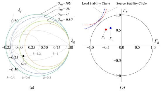
Figure 1.
(a) Gain-plane with the constant-GME circles (colored solid) and constant-k contours (grey dashed). (b) Reflection-coefficient-plane.
Although the λ-plane can provide the gain state of an A2P, it gives little information about the stability of the A2P terminals. This deficiency can be filled by the reflection-coefficient-plane. For a GME-based A2P, the source and load admittances are completely determined by Equations (2) and (3). It is convenient to convert them to the reflection coefficient Γ and plot on the Γ-plane to observe the stability states of the A2P terminals. Figure 1b plots the coordinates of ΓL and ΓS for the 40 nm NMOS transistor at 200 GHz on the Γ-plane with the load and source stability circles. The load and source stability circles identify the output and input unstable regions, respectively. If ΓL falls into the output unstable region, the real part of the input impedance of A2P become negative, and conjugated matching at the input port becomes impossible. In this case, GME is impossible to realize. If ΓS falls into the input unstable region, the real part of the output impedance becomes negative, and the GME-based A2P becomes an oscillator.
Utilizing both the λ- and Γ-planes, the precise gain and stability states of a GME-based A2P can be observed simultaneously, and the GME-based amplifier can now be visually optimized.
3. Movement on the Planes by Feedback Circuits
3.1. Parallel Embedding
Applying feedback networks to A2P leads to the movements on both the λ- and Γ-planes. Figure 2a shows the parallel embedding (also called Y embedding). A passive component is added between the input and output terminals of the A2P to form a new embedded A2P. The Y matrix of the embedded A2P is
where the quote denotes the Y parameters of the original A2P, and jBY is the admittance of the embedded component. For the λ-plane, let λ’ be the inverse gain of the original A2P; the inverse gain of the embedded A2P is written as
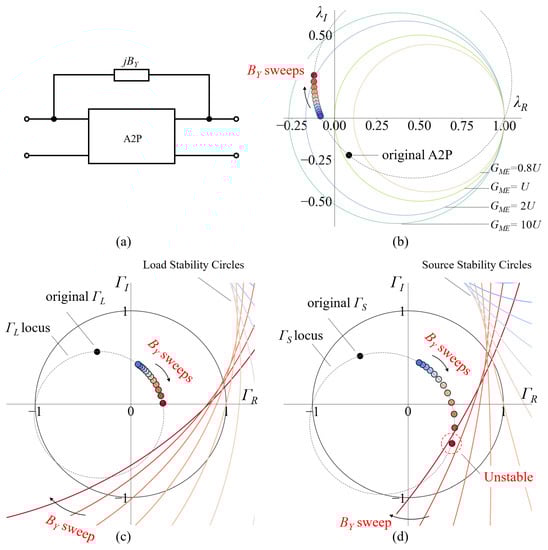
Figure 2.
Parallel embedding. (a) A2P embedded by parallel embedding. (b) Movement of the A2P on the gain-plane caused by parallel embedding. (c) Movement of ΓL and load stability circles of the A2P on the load reflection-coefficient-plane. (d) Movement of ΓS and source stability circles of the A2P on the source reflection-coefficient-plane. The circles in colormap from blue to red are the load and source stability circles when BY is swept in (c,d), respectively. Please kindly note that they are labeled by the text “Load Stability Circles” in (c) and “Source Stability Circles” in (d).
When BY is swept, the coordinate of the embedded A2P on the λ-plane moves accordingly. It is derived by Shuhei Amakawa that the locus of the embedded A2P can be written as []:
where Y21 = r + jq. Equation (11) denotes a circle on the λ-plane, as shown in Figure 2b. Note that the radius and center of the circle depend on the original A2P. This indicates that for a given A2P, the achievable position by applying parallel embedding is limited on this circle.
For the Γ-plane, the load reflection ecoefficiency ΓL of the embedded A2P is written as
where Y0 is the port admittance. Applying Equations (2) and (9) into Equation (12), ΓL can be rewritten as
where
Equation (13) denotes the locus of ΓL of the embedded A2P on the ΓL-Plane when BY is swept. The locus and a group of load stability circles with the swept BY are plotted in Figure 2c. Similar results on ΓS are obtained and shown in Figure 2d. It can be observed from Figure 2 that sweep of BY alters the distance between ΓL and the load stability circle as well as the distance between ΓS and the source stability circle. With certain BY, the input or output terminal of the embedded A2P becomes unstable. Note that when the embedded A2P is moved to the position with higher GME on the λ-plane, its ΓL and ΓS are moved closer to the load and source stability circles on the Γ-plane, respectively.
3.2. Series Embedding
Figure 3a shows the series embedding (also called Z embedding). A passive component is added in series with the common terminal of the A2P to form a new embedded A2P. The Z matrix of the embedded A2P is
where the quote denotes the Z parameters of the original A2P, and jXZ is the impedance of the embedded component. For the λ-plane, the locus of the embedded A2P when XZ is swept is written as
where Z21′= c + jd. The locus is plotted in Figure 3b.
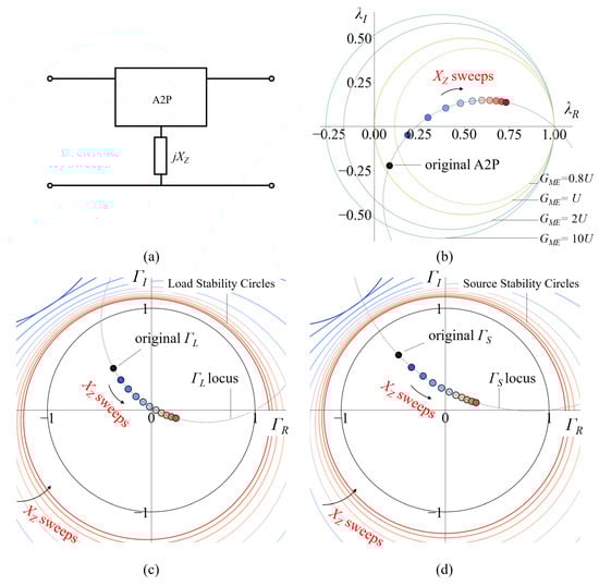
Figure 3.
Series embedding. (a) A2P embedded by series embedding. (b) Movement of the A2P on the gain-plane caused by series embedding. (c) Movement of ΓL and load stability circles of the A2P on the load reflection-coefficient-plane. (d) Movement of ΓS and source stability circles of the A2P on the source reflection-coefficient-plane. The circles in colormap from blue to red are the load and source stability circles when XZ is swept in (c,d), respectively. Please kindly note that they are labeled by the text “Load Stability Circles” in (c) and “Source Stability Circles” in (d).
For the Γ-plane, ΓL of the embedded A2P is written as
where Z0 is the port impedance. Applying Equations (4) and (14) into (16), ΓL can be rewritten as
where
Equation (17) denotes the locus of ΓL of the embedded A2P on the ΓL-Plane when XZ is swept, as shown in Figure 3c. Similar results on the ΓS-Plane are obtained and shown in Figure 3d. It is observed that series embedding provides a phase of movements on the λ-and Γ-planes that is different from parallel embedding.
3.3. Combined Embedding
Simple parallel or series embedding can only provide limited range of movement for the A2P on the λ-plane, making it difficult for an A2P to move to the optimized-GME position. To expand the range of movement, parallel and series embedding can be applied successively to an A2P to provide a two-step movement on the λ-plane [,]. However, this embedding may impose some limitations in terms of loss, DC bias, or isolation on the embedded A2P []. Another embedding structure that can broaden the scope of movement is cascade embedding. The idea is to cascade passive components to the A2P before parallel or series embedding is applied. The cascading components form a new cascaded A2P with the original A2P. The network parameters of the cascaded A2P are manipulated by the cascading components. It is revealed by Equations (11) and (13) that in parallel or series embedding, the locus of the embedded A2P on the λ-plane depends on the network parameters of the original A2P. Therefore, when parallel or series embedding is applied to the cascaded A2P, the locus of the final A2P can be altered by the cascading components. The range of movement on the λ-plane is thus widely expanded.
Consider a cascade–parallel embedding in Figure 4a. Two passive components are cascaded to the A2P before the parallel component is added. The Y matrix of the cascaded A2P is
where jX1 and jX2 are the impedances of the cascaded components, and the single quote and double quotes denote the Y parameters of the original and cascaded A2P, respectively. |Y| = Y12Y21 − Y11Y22. The Y matrix of the parallel-embedded A2P is
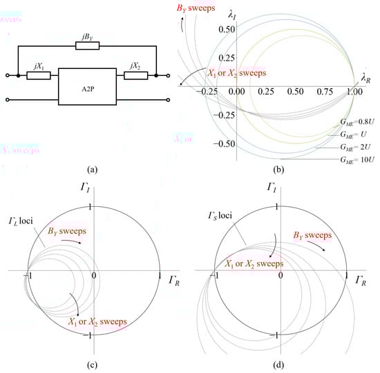
Figure 4.
Cascade–parallel embedding. (a) A2P embedded by cascade–parallel embedding. (b) Movement of the A2P on the gain-plane caused by cascade–parallel embedding. (c) Movement of ΓL of the A2P on the load reflection-coefficient-plane. (d) Movement of ΓS of the A2P on the source reflection-coefficient-plane.
For the λ-plane, replacing Y21’ and λ’ in Equation (10) with Y21’ and “λ” in Equation (18), the locus of the embedded A2P on the plane when BY is swept is written as
where
Yij’ = Gij’ + jBij’ is the Y parameter of the original A2P. Note that now the center and radius of the circle are a function of X1 and X2. Therefore, by manipulating the value of X1 and X2, the achievable coordinates for the embedded A2P are now widely expanded, as shown in Figure 4b.
For the Γ-plane, replacing Yij’ in Equation (13) with Yij’ in Equation (18), the loci of ΓL of the embedded A2P when X1, X2, and BY are swept can be derived. Again, similar results can be obtained for the loci of ΓS. Figure 4c and 4d plot the loci on the ΓL- and ΓS-planes with different X1 and X2, respectively.
4. Flowchart for GME Optimization
With the knowledge of visually analyzing the gain and stability states of a GME-based A2P and the methods for manipulating the movements of the A2P on the λ-plane and Γ-plane, a design process for optimizing the GME of an amplifier is developed, as shown in Figure 5.
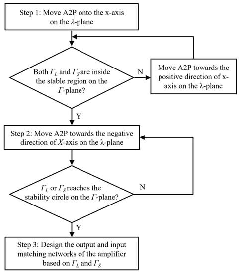
Figure 5.
Flowchart of the process for optimizing the GME of an amplifier.
According to above analysis, the optimal position of GME of an amplifier, at which the value of GME reaches its maximum while both the input and output ports of the amplifier remain stable, is located on the X-axis of the λ-plane. Consequently, the main idea of optimization is to move A2P onto the X-axis and then gradually move it towards the negative direction of the X-axis until one of ΓL or ΓS reaches the stability circle. In this state, any slight movement of A2P towards the negative direction of the X-axis on the λ-plane will push ΓL or ΓS into the unstable region on the Γ-plane. This means that GME has reached its maximum value for an amplifier and cannot be improved any further; i.e., the GME is optimized. Note that one decision point is added between step 1 and step 2 in the flowchart to prevent the case that the A2P is already unstable after being moved onto the X-axis on the λ-plane.
To exhibit the details of the proposed process of optimizing GME, an example of a 40 nm CMOS GME-based amplifier is designed and optimized at 200 GHz. A common-source NMOS transistor with a gate width of 32 μm is used as the original A2P. The Gmax and k of the transistor are 3.58 dB and 1.19, respectively.
In step 1, an inductor and a capacitor are parallelly embedded to the transistor to move the embedded transistor onto the X-axis on the λ-plane. ΓL and ΓS of the embedded transistor are calculated using Equations (2) and (3) and confirmed to be within the stable region. In step 2, two cascading inductors are added to the transistor and form a cascade–parallel embedding to broaden the scope of movement of the transistor on the λ-plane. The values of the embedding components are adjusted to move the transistor towards the negative direction of the X-axis on the λ-plane. The movements of ΓL and ΓS on the Γ-plane are observed simultaneously. When Step 2 is repeated for the third time, ΓS reaches the source stability circle on the Γ-plane, and thus the transistor reaches the optimum position for GME on the λ-plane. The movement of the transistor on the λ-plane and the movements of ΓL and ΓS of the transistor on the Γ-plane are shown in Figure 6b–6d, respectively. Note that it is ΓS that reaches the stability circle in this example. The values of the embedding components and GME of the transistor following each step are shown in Table 1. The GME of the embedded transistor is boosted to 7.68 dB. The k of the embedded transistor is now 0.601, and Gmax is no longer available as the transistor is in the potential unstable state. The stronger robustness of GME compared to Gmax is thus reflected. The circuit schematic of the optimum embedded transistor is shown in Figure 6a. The YL and YS of the embedded transistor are calculated using Equations (2) and (3), and the output and input matching networks are designed accordingly.
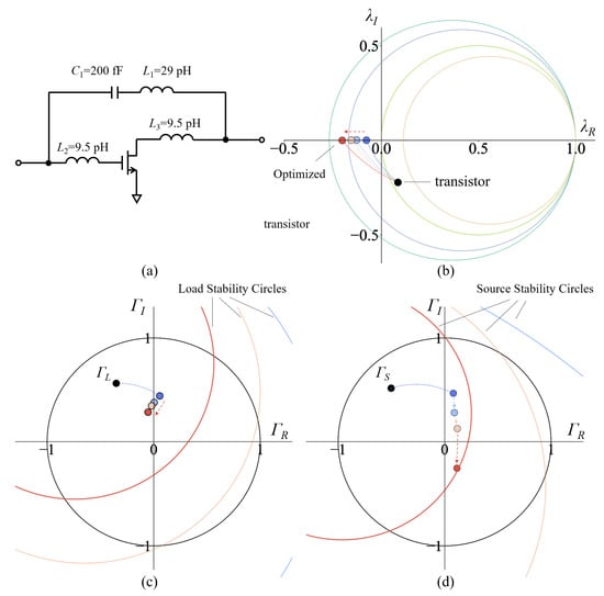
Figure 6.
Process of optimizing the GME of the transistor. (a) Transistor embedded by the optimum embedding. (b) Movement of the embedded transistor on the gain-plane in the optimizing process. (c) Movement of ΓL and load stability circles of the embedded transistor on the load reflection-coefficient-plane. (d) Movement of ΓS and source stability circles of the embedded transistor on the source reflection-coefficient-plane. The lines in different colors in (c,d) are the load stability circles and source stability circles, respectively. They are labelded by the texts.

Table 1.
The values of the embedding components and GME of the embedded transistor following each step in the process.
In this optimization method, the amplifier is pushed to the edge between stability and instability in order to obtain the maximum GME at the design frequency. This may lead to a small bandwidth of the amplifier. In practical design, compromising between high gain and large bandwidth is necessary. The final GME-based amplifier and the simulated S parameters are shown in Figure 7. After the compromise for bandwidth, a peak small signal gain of 6.7 dB is obtained. Both S11 and S22 are less than 0 dB at a large frequency range from 150 GHz to 250 GHz, indicating that both the input and output terminals of the amplifier stay stable.
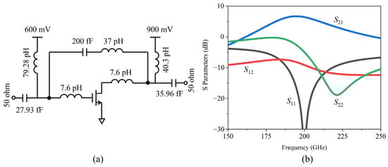
Figure 7.
The optimized 200 GHz GME-based amplifier. (a) The circuit schematic of the amplifier. (b) The S parameters of the amplifier.
5. Implemented Amplifier and Measurement Results
Using the proposed GME optimization process, a two-stage GME-based differential embedded amplifier is designed and fabricated in a 40 nm CMOS technology at 210 GHz.
The GME core of the amplifier is shown in Figure 8a. Two identical nmos transistors are used to form a differential transistor pair. The transistor has a channel length of 40 nm and a total width of 32 μm with 32 fingers. The bias condition is VGS = 600 mV; VDS = 900 mV. The fmax of the transistor is 284 GHz. The Gmax and k of the transistor are 3.58 dB and 1.19, respectively. A pair of cross-connected capacitors and four transmission lines with characteristic impedance of 50 ohm are applied to the transistor pair to form the embedding and boost GME. The neutralizing capacitor Cn of 19.5 fF equivalently introduces a negative admittance of −0.027 j ohm across gate and drain terminals of the transistor [], as shown in Figure 8b. Cn, TL1, and TL2 together form a cascade–parallel embedding and boost the GME of the transistor to a desired value of 6.53 dB, as shown in Figure 8c. The movements of ΓL and ΓS of the core by the embedding are shown in Figure 8d.
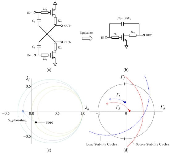
Figure 8.
The core of the 210 GHz two-stage GME-based differential embedded amplifier. (a) Circuit schematic of the core. (b) Circuit schematic of the equivalent single-ended circuit for the core. (c) Movement of the core on the gain-plane caused by the embedding. (d) Movement of ΓL and ΓS of the core on the reflection-coefficient-plane.
The circuit schematic of the amplifier is shown in Figure 9a. The input/output matching and interstage matching are implemented using transmission lines with characteristic impedance of 50 ohm and metal-oxide-metal capacitors. Figure 9b shows the micrograph of the amplifier. A pair of baluns are introduced to the input and output terminals for single-ended-differential conversion. The chip size is 0.73 × 0.79 mm2. As shown in Figure 9c, the amplifier has a maximum measured small-signal gain of 10.48 dB at 195.33 GHz; the small-signal gain at 210 GHz is 9.53 dB. The large-signal measurement is shown in Figure 9d; the measured maximum output power is 3.04 dBm, and the large-signal gain is 7.08 dB at 210 GHz. The power consumption is 41.4 mW with a 0.9 V supply voltage.
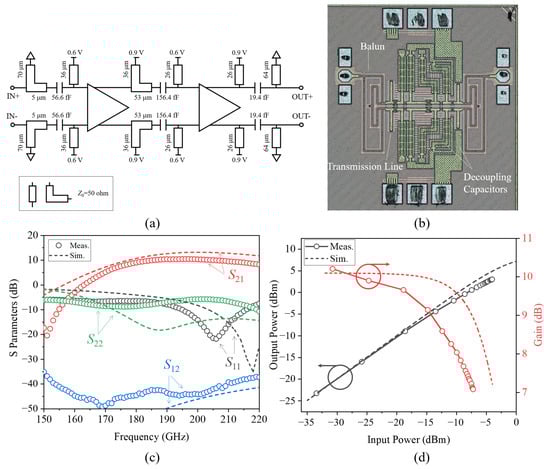
Figure 9.
The 210 GHz two-stage GME-based differential embedded amplifier. (a) Circuit schematic. (b) Chip microphotograph. (c) Measured and simulated S parameters. (d) Measured and simulated output power (labeled by the left arrow) and large-signal gain (labeled by the right arrow).
There are two main reasons that lead to the differences between the simulation and experiment results. The first reason is that there are differences between the simulated circuit characteristics and the actual circuit characteristics, including differences in transistors, transmission lines, MOM capacitors, and so on. These differences lead to changes in the matching state of the amplifier, resulting in differences between the simulated and measured S parameter results in Figure 9c. The second reason is that the baluns for single-ended-differential conversion in both input and output terminals of the amplifier introduce additional insertion loss, resulting in performance degradation in the measured results.
6. Conclusions
This paper presents a graphical process for optimizing the maximally efficient gain GME of a near-fmax A2P utilizing both the gain-plane and the reflection-coefficient-plane. The optimum GME is obtained by moving the A2P to a specific position on the X-axis of the gain-plane while maintaining ΓL and ΓS of the A2P within the stable regions of the reflection-coefficient-plane. The movements on both planes are achieved by parallel, series, or cascaded embedding components. These embeddings are calculated and visually analyzed. Details of the optimizing process are exhibited. To show the feasibility of the process, a two-stage embedded amplifier is implemented in a 40 nm CMOS technology with a measured small-signal gain of 10.48 dB at 195.33 GHz.
Author Contributions
Y.X.: Methodology, Software, Investigation, Data Curation, and Writing. R.D.: Conceptualization, Supervision, and Investigation. All authors have read and agreed to the published version of the manuscript.
Funding
This research was performed at the Chinese Academy of Science Terahertz Science Center, and was funded by the National Natural Science Foundation of China (No. 61988102), the Science and Technology Planning Project of Guangdong Province, China (No. 2019B090909011), the Key Research and Development Program of Guangdong Province, China (No. 2019B090917007), and the Guangzhou Basic and Applied Basic Research project (No. 2023A04J0334).
Data Availability Statement
The data that support the findings of this study are available from the corresponding author upon reasonable request.
Conflicts of Interest
The authors declare no conflict of interest.
References
- Lee, S.; Hara, S.; Yoshida, T.; Amakawa, S.; Dong, R.; Kasamatsu, A.; Sato, J.; Fujishima, M. An 80-Gb/s 300-GHz-band single-chip CMOS transceiver. IEEE J. Solid-State Circuits 2019, 54, 3577–3588. [Google Scholar] [CrossRef]
- Cooper, K.B.; Dengler, R.J.; Llombart, N.; Thomas, B.; Chattopadhyay, G.; Siegel, P.H. THz imaging radar for standoff personnel screening. IEEE Trans. Terahertz Sci. Technol. 2011, 1, 169–182. [Google Scholar] [CrossRef]
- Zhou, D.; Hou, L.; Xie, W.; Zang, Y.; Lu, B.; Chen, J.; Wu, P. Practical dual-band terahertz imaging system. Appl. Opt. 2017, 56, 3148–3154. [Google Scholar] [CrossRef] [PubMed]
- Heydari, P. Terahertz integrated circuits and systems for high-speed wireless communications: Challenges and design perspectives. IEEE Open J. Solid-State Circuits Soc. 2021, 1, 18–36. [Google Scholar] [CrossRef]
- Bameri, H.; Momeni, O. A high-gain mm-wave amplifier design: An analytical approach to power gain boosting. IEEE J. Solid-State Circuits 2017, 52, 357–370. [Google Scholar] [CrossRef]
- Amakawa, S. Graphical approach to analysis and design of gain-boosted near-f max feedback amplifiers. In Proceedings of the 2016 46th European Microwave Conference, London, UK, 4–6 October 2016; pp. 1039–1042. [Google Scholar]
- Kotzebue, K.L. Maximally efficient gain: A figure of merit for linear active 2-ports. Electron. Lett. 1976, 19, 490–491. [Google Scholar] [CrossRef]
- Kotzebue, K.L. Microwave-transistor power-amplifier design by largesignal y parameters. Electron. Lett. 1975, 11, 240–241. [Google Scholar] [CrossRef]
- Kotzebue, K.L. A quasi-linear approach to the design of microwave transistor power amplifiers. IEEE Trans. Microw. Theory Tech. 1976, 24, 975–978. [Google Scholar] [CrossRef]
- Momeni, O.; Afshari, E. A high gain 107 GHz amplifier in 130 nm CMOS. In Proceedings of the 2011 IEEE Custom Integrated Circuits Conference, San Jose, CA, USA, 19–21 September 2011; pp. 1–4. [Google Scholar]
- Khatibi, H.; Khiyabani, S.; Cathelin, A.; Afshari, E. A 195 GHz single-transistor fundamental VCO with 15.3% DC-to-RF efficiency, 4.5 mW output power, phase noise FoM of−197 dBc/Hz and 1.1% tuning range in a 55 nm SiGe process. In Proceedings of the 2017 IEEE Radio Frequency Integrated Circuits Symposium, Honolulu, HI, USA, 4–6 June 2017; pp. 152–155. [Google Scholar]
- Johnson, K.M. Large signal GaAs MESFET oscillator design. IEEE Trans. Microw. Theory Tech. 1979, 27, 217–227. [Google Scholar] [CrossRef]
- Wang, Z.; Heydari, P. A study of operating condition and design methods to achieve the upper limit of power gain in amplifiers at near-fmax frequencies. IEEE Trans. Circuits Syst. I Regul. Pap. 2017, 64, 261–271. [Google Scholar] [CrossRef]
Disclaimer/Publisher’s Note: The statements, opinions and data contained in all publications are solely those of the individual author(s) and contributor(s) and not of MDPI and/or the editor(s). MDPI and/or the editor(s) disclaim responsibility for any injury to people or property resulting from any ideas, methods, instructions or products referred to in the content. |
© 2023 by the authors. Licensee MDPI, Basel, Switzerland. This article is an open access article distributed under the terms and conditions of the Creative Commons Attribution (CC BY) license (https://creativecommons.org/licenses/by/4.0/).