1. Introduction
Bandpass filters (BPFs) and rat-race couplers (RCs) are essential components in the RF/microwave front end of wireless communication systems [
1,
2,
3,
4,
5,
6,
7,
8]. In general, BPFs and RCs are designed separately and then cascaded for power dividing/combining and signal selecting. This results in the disadvantages of large size, high loss, and mismatching. As a good solution, multifunctional filtering rat-race couplers (FRCs) have been presented and paid much attention.
In recent years, many efforts have been conducted to integrate RCs and BPFs as multifunctional FRCs. In general, resonators [
9,
10,
11] are loaded on traditional RCs for realizing filtering responses. However, the obvious drawback is the overly narrow bandwidth. As observed in [
9,
10,
11], the bandwidths were all less than <5%. For bandwidth improvement, filtering sections are usually used to replace the transmission lines (TLs) in the RC. In [
12], four ±
K-inverters with the bandpass function were utilized to replace the TLs in a conventional RC. Measurement results showed that the fractional bandwidth (FBW) was increased to 13% with a wide stopband. In [
13], an FRC with about 13% FBW was designed by using the coupled multi-line filtering section to replace the TLs in a conventional RC. In [
14], an FRC based on an eight-line spatially symmetrical coupled structure was proposed and implemented in low-temperature co-fired ceramic (LTCC) technology. The measured FBW was 14%. In [
15], a circular patch resonator was applied in designing the FRC, and an FBW of 13.1% was obtained.
Although the bandwidths for the FRCs introduced above were improved to some degree, they were still not enough for a wideband communication system. To further increase the operation bandwidth, several methods were proposed [
16,
17,
18,
19]. Although the FBWs of these RCs were further enlarged, the filtering performance was ignored and not merged into the RC. Until now, few studies in the literature have reported the designing of wideband FRCs. In [
20,
21], by using short-circuited stubs and filtering sub-circuits, FRCs with equal and unequal power division ratios were presented, where the measured FBWs could reach around 100%. However, since several coupled lines with tight coupling were needed in the structure, the FRCs cannot be implemented on a single-layer substrate. Additionally, the out-of-band performance was not provided. Similarly, a series of wideband FRCs with an FBW of 35.2% and an out-of-band rejection of more than 20 dB were presented in [
22]. However, the output ports’ phase performances need to be improved.
In this study, a compact wideband FRC based on a shared triple-mode resonator is presented. By cascading two groups of triple-mode resonators to the input and isolation ports of the RC, a wide bandpass filtering response can be obtained. Additionally, two extra transmission zeros (TZs) were achieved by shunting the open-circuited TLs to the output ports of the RC. For validation, a prototype was designed and fabricated. It exhibited a wide FBW of more than 60%, a high selectivity with a rectangular coefficient (|BW
30dB/BW
3dB|) equal to 1.49, a low Insertion Loss (IL) of less than 1 dB, and a wide stopband extending to 2.56
f0. The theoretical analysis of the proposed FRC is illustrated in
Section 2.
Section 3 gives the implementation and measurement results, followed by a conclusion in
Section 4.
2. Theoretical Analysis
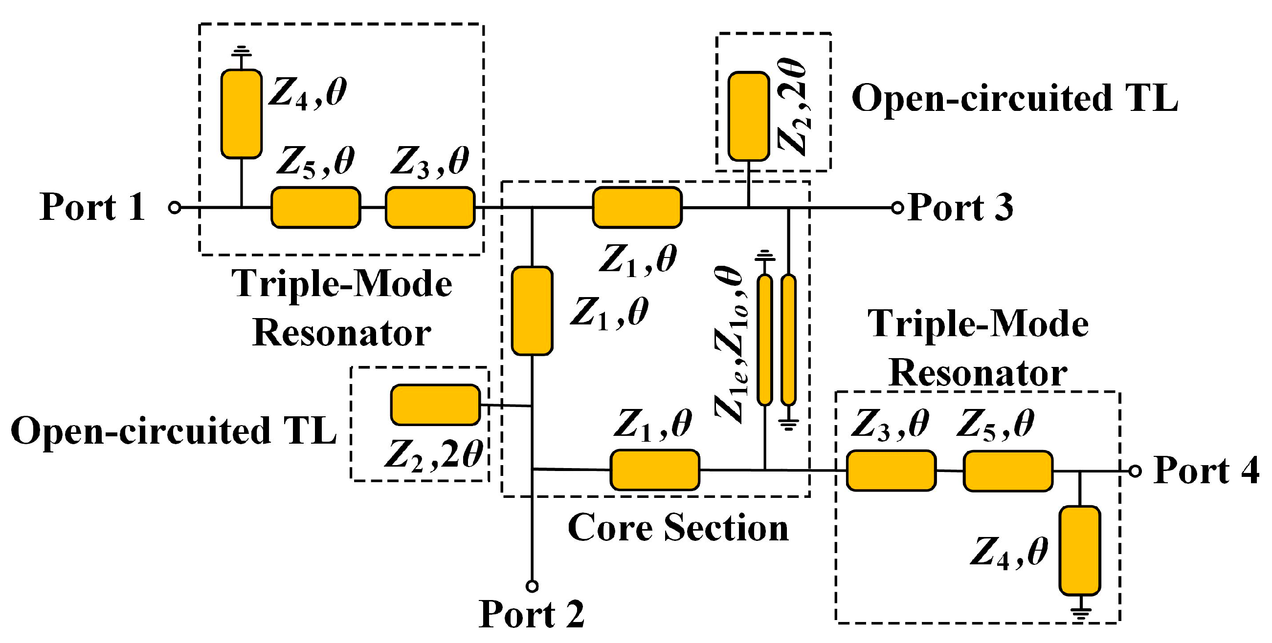
The schematic of the proposed wideband FRC is shown in
Figure 1. The proposed wideband FRC consisted of two leading triple-mode resonators, one core section, and two
λ/2 open-circuited TLs. The core of the proposed FRC was composed of three sections of
λ/4 TLs and one section with a
λ/4 short-circuited parallel coupled line (CL). In ports 1 and 4 of the FRC, two groups of leading triple-mode resonators with the same parameters were cascaded. Additionally, two
λ/2 open-circuited TLs were shunted on ports 2 and 3 separately. It was noted that the filtering performance was realized by the cooperation of the leading triple-mode resonator, the
λ/4 TL/CL at the core of the FRC, and the
λ/2 open-circuited TL. The leading triple-mode resonator was a shared component of the two signal paths from the input port to the two output ports. When combining the triple-mode resonator with the
λ/4 TL/CL at the core of the FRC, four transmission poles (TPs) could be generated. In addition, two extra TZs could be obtained by loading the
λ/2 open-circuited TL on the two output ports of the RC.
The characteristic impedances of the
λ/4 TL and the
λ/2 open-circuited TL are defined as
Z1 and
Z2, respectively, while the even- and odd-mode characteristic impedances of the
λ/4 short-circuited parallel CL are named
Z1e and
Z1o separately. The triple-mode resonator is constructed of one
λ/4 short-circuited stub with the characteristic impedance of
Z4, and two
λ/4 TLs with the characteristic impedances of
Z5 and
Z3. Let
θ be the electrical length of the CL, which is equal to 90° at the center frequency of
f0. Since the proposed structure is half-symmetric, not full-symmetric, the traditional even-odd mode decomposition method cannot be applied. In order to analyze the proposed circuit, the method introduced in [
23] is utilized, which considers the RC as the combination of an in-phase power divider and an out-of-phase power divider. It is noted that according to [
23], the in-phase case is called the even mode, and the out-of-phase case is named the odd mode, which is different from the commonly used even-odd mode decomposition method.
Before the decomposition, twice equivalent processes are applied in order to simplify the analysis. Firstly, the
λ/4 short-circuited parallel CL is equivalent to a TL with an electrical length of 3
λ/4. In the following, the relations between the
λ/4 short-circuited parallel CL and the 3
λ/4 TL are derived. Based on the TL theory and the four-port impedance matrix of CLs, the input impedances of the TL and the CL can be expressed as (1a) and (1b), respectively.
where
In the above equations, θ is the electrical length of the CL, which is equal to 90° at the center frequency of f0. This means that the equivalent process is established at the center frequency. By equalizing (1a) with (1b) at arbitrary terminal impedance ZT, the value of the Z1 is derived to be equal to 1/Y1b. Thus, when Y1b·Z1 = 1, the λ/4 short-circuited parallel CL can be equivalent to the 3λ/4 TL at the center frequency.
Figure 2 shows the schematic of the proposed wideband FRC under one equivalent process. The difference between
Figure 1 and
Figure 2 is to replace the
λ/4 short-circuited parallel CL with the 3
λ/4 TL. According to
Figure 2, the even- and odd-mode decomposition method for the half-symmetric circuit can be applied. Firstly, ports 2 and 3 are under even-mode excitation. Since the signals that arrive at node
P have equal magnitude and phase performance, they sum together at port 1. When two signals with equal magnitude and opposite phases reach node Q, port 4 with isolation performance is realized. Secondly, ports 2 and 3 are under even-mode excitation. Since the signals that arrive at node
P have equal magnitude and opposite phase performance, they cancel at port 1. Thus, port 1 is the isolation port. While the two signals that reach node Q are with equal magnitude and phase, the signals that reach port 4 are sum together.
Under the second equivalent process, the values of tan 3
θ and tan
θ are equivalent to each other at the center frequency of
f0 based on the relation of tan (π +
θ) = tan
θ. Here,
θ is designated as 90° at the center frequency. Therefore, the 3
λ/4 TL is equivalent to the
λ/4 TL at the center frequency
f0. Thus, the even- and odd-mode equivalent circuits of the presented FRC can be depicted in
Figure 3.
The twice-equivalent processes are beneficial for analyzing the proposed circuit. It is observed in
Figure 3 that the proposed FRC after twice equivalent processes is symmetrical along the diagonal line (
AA′). Thus, one equivalent circuit is enough in the analysis. This will simplify the analysis. In the following, the even-mode excitation is utilized, where the equivalent circuit is shown in
Figure 3a. According to
Figure 3a, the
ABCD matrix between ports 1 and 2 can be expressed as (3a)–(3d) [
22].
Since port 4 is isolated under even-mode excitation, the reflection and transmission coefficients (
S11 and
S21) can be extracted as
Here, Z0 is the system impedance, and Zine is the input impedance at port 1 under even-mode excitation. According to (4), the parameters of the proposed FRC can be obtained by assigning several conditions related to the filtering performance.
Firstly, the case of generating the TZs is introduced. In the calculation of the TZs, the value of
S21 should be equal to 0. This indicates that the signal is fully reflected at port 2. When shunting the open-circuited TL, the input impedance
Zopen of the open-circuited TL can be obtained using (6). Here,
θ corresponds to the electrical length at the center frequency of
f0, which equals 90°. The
f1 denotes the operating frequency. When
Zopen = 0, the condition of full reflection can be satisfied. According to (6),
f1 is calculated as 0.5
f0 and 1.5
f0. Thus, two TZs at 0.5
f0 and 1.5
f0 can be obtained when shunting the open-circuited TL.
Secondly, the case of generating TPs is investigated. In the calculation of the TPs, the
S11 should be equal to 0. According to (4), it is found that to satisfy
S11 = 0, the real and imaginary parts of
Zine should be equal to 50 Ω and 0, respectively, as (7a) and (7b) expresses.
Substitute the expressions in (3a)–(3d) into (7a) and (7b), and the equation in (8) can be derived, where the complicated expressions of
x1,
x2,
x3,
x4,
x5,
x6,
x7,
x8,
x9,
x10, and
x11 are listed in
Appendix A.
According to (8), the different TPs which are related to the circuit parameters can be calculated. It is observed in (8) that the equation is of higher order. Although it can be treated as a quintic equation, there is still no radical solution. It is known that the radical solution is limited to the fourth-order equation. In the design, to obtain the circuit parameters of the FRC, a numerical algorithm is applied to the calculation.
Figure 4 shows the calculated TPs versus different circuit impedances (
Z1,
Z2,
Z3,
Z4,
Z5) according to (8). It is noted that when one circuit parameter is investigated, other circuit parameters are at their optimized values. Besides, these curves are based on the twice equivalent processes, which are established at the center frequency. For simplicity calculation, the condition of
Z2 =
Z1 is applied. Since the two TZs are located at 0.5
f0 and 1.5
f0, the TPs should be within this bandwidth. Thus, the frequency range of the TPs is set as 0.6
f0 to 1.4
f0. Firstly, it is seen in
Figure 4 that four TPs can be generated in the operation bandwidth. Here, three of the TPs are generated by the shared leading triple-mode resonator; the other is induced by the
λ/4 TL/CL in the core of the FRC. In the following, the influences of the circuit impedances (
Z1,
Z2,
Z3,
Z4,
Z5) are discussed separately.
It is observed from
Figure 4a that when the value of
Z1 (
Z2) is less than 75 Ω, there are only two TPs. As
Z1 (
Z2) increases, four TPs are generated. Here, the
ftp1 and
ftp4 are constant, along with the changing of
Z1 (
Z2), while the corresponding
ftp2 and
ftp3 are increased and decreased separately when
Z1 (
Z2) increases. The two TPs finally merged when
Z1 (
Z2) was larger than 110 Ω. In summary, when
Z1 (
Z2) is in the range of 75~105 Ω, four TPs appear within 0.6 − 1.4
f0. Beyond this range, the in-band TPs are reduced to less than four. As seen from
Figure 4b, the
ftp2 and
ftp4 are decreased along with the increase of
Z3. In contrast,
ftp1 and
ftp3 are in the opposite trend. Four TPs appear when
Z3 is within 122~153 Ω. When
Z3 is less than 122 Ω, the TPs are reduced to three. When
Z3 is larger than 153 Ω, the TPs are reduced to two.
Figure 4c shows the influence of
Z4. When
Z4 is less than 4 Ω, there is only one TP in the operating bandwidth. When
Z4 is in the range of 20~40 Ω, the four TPs appear in the operating band, and they are nearly stable as
Z4 increases. When
Z4 is larger than about 45 Ω, the
ftp3 and
ftp4 are merged into one TP. Similar merging is also observed for
ftp2 and
ftp1. Thus, two in-band TPs can be obtained. As illustrated in
Figure 4d, four TPs are generated when
Z5 is in the range of 76~100 Ω. While as
Z5 increases, the
ftp2 and
ftp4 are increased, and the
ftp1 and
ftp3 are decreased. It is concluded that
Z1,
Z2, and
Z5 have a similar influence on the TPs, while
Z3 exhibits the nearly opposite trend with
Z1,
Z2, and
Z5. The changing of
Z4 has less effect on the TPs.
To illustrate more clearly, the calculated |
S11| of the even-mode equivalent circuit (according to
Figure 3a) with different groups of circuit parameters are plotted in
Figure 5. It can be seen that the provided curves all satisfy the criterion of |
S11| < −10 dB (more than 10 dB return loss). When the more strictly condition of |
S11| < −15 dB is assigned, the parameters of
Z1 =
Z2 = 90 Ω,
Z3 = 136 Ω,
Z4 = 36 Ω, and
Z5 = 92 Ω are eligible. Thus, this group of parameters is selected for the proposed circuit. Here, the parameters are for the circuit with twice equivalent processes where the
λ/4 short-circuited parallel CL is equivalent to the
λ/4 TL. To calculate the final circuit parameters, the relations in (1a) and (1b) are utilized, which indicates that the
λ/4 short-circuited parallel CL can be equivalent to the 3
λ/4 TL when Y
1b·Z1 = 1. Then, the values of
Z1e and
Z1o in the CL are calculated as 220 Ω and 40 Ω, respectively.
Table 1 shows the final calculated results of the designed FRC, which corresponds to the schematic in
Figure 1.
Figure 6 shows the theoretical frequency responses of the designed FRC. Under the criteria of 10 dB return loss, the FBWs at ports 1 and 4 excitations are 70% and 62.1%, respectively, while the 3 dB FBWs reach 78.6% and 72.9%, separately. The isolations of the FRC are both larger than 20 dB across the whole frequency band shown. Besides, under the condition of a 10 dB out-of-band rejection level, the band extends to 2.57
f0. From 0.99 GHz to 1.80 GHz, the output ports amplitude imbalances (APIs) are less than 1 dB, and the phase difference (PD) errors are within ±5° for ports 1 and 4 excitations.
The design procedures of the proposed FRC are listed below as guidance.
- (1)
Determine the designed center frequency f0 and two TZs located at 0.5 f0 and 1.5 f0 can be obtained by loading the λ/2 open-circuited TL;
- (2)
According to (8), the variations of the in-band TPs versus different impedances (Z1, Z2, Z3, Z4, Z5) can be plotted, and suitable groups of values can be chosen in consideration of symmetrical distributed TPs;
- (3)
According to the obtained groups of circuit parameters, the |S11| of the even/odd mode equivalent circuit can be plotted, and the values can be finally determined by specified in-band |S11| criteria, such as 10 dB or 15 dB;
- (4)
Using the relations in (1a) and (1b), which indicates that the λ/4 short-circuited parallel CL can be equivalent to the 3λ/4 TL at the center frequency, the final parameters for the λ/4 short-circuited parallel CL can be obtained;
- (5)
Transform the circuit parameters to physical dimensions. Perform layout simulation of the whole circuit structure in an electromagnetic simulator, and make suitable adjustments to obtain better results.
3. Implementation and Measurement
For validation, a prototype operating at the center frequency of 1.4 GHz is designed and fabricated. The substrate is chosen as the F4BM with a permittivity of 3, a loss tangent of 0.001, and a thickness of 1.5 mm since the F4BM substrate has a lower loss than the FR4 substrate (the loss tangent of 0.02). Moreover, it is cheaper than the low-loss Rogers substrate. Thus, the F4BM is a favored substrate for fabricating microwave circuits.
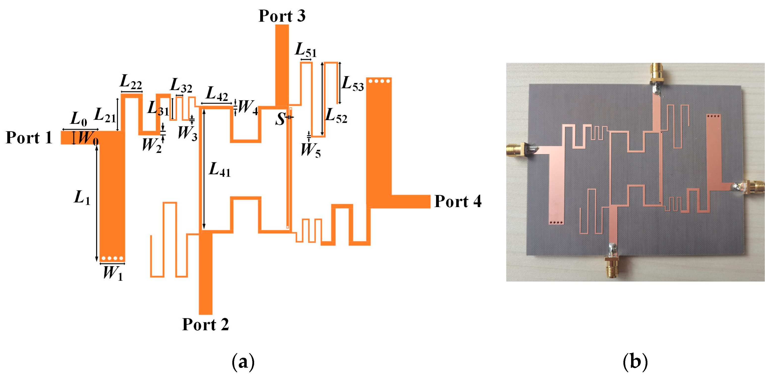
Figure 7 shows the layout and photograph of the fabricated FRC. The dimension variables are also labeled in
Figure 7. It is noted that for size reduction, meander lines are used in the implementation, including the TLs in the leading triple-mode resonators, the TL in the core section, and the
λ/2 open-circuited TLs. The overall size of the fabricated prototype is 101 mm × 80 mm, which corresponds to 0.48
λg × 0.38
λg (
λg is the guide wavelength of a 50 Ω microstrip line at the center frequency of 1.4 GHz). After optimization using the simulator Ansoft HFSS, the final dimensions of the fabricated prototype can be obtained, as illustrated in
Table 2.
Figure 8a shows the simulated and measured input impedance matching and output port distributions of the designed prototype under port 1 excitations. It is observed that the measured bandwidth for |
S11| < −10 dB under port 1 excitation is in the range of 0.95~2.02 GHz, yielding an FBW of 75.7%. In this bandwidth, the measured API is less than 1 dB. Under the criterion of 3 dB output port distributions, the measured FBW reaches 81.4% (from 0.89 to 2.03 GHz). Moreover, the measured rectangular coefficient (|BW
30dB/BW
3dB|) is 1.49, which indicates the feature of high selectivity. In the out-of-band, the suppression level is larger than 13 dB. While for 10 dB out-of-band rejection, the measured bandwidth extends to 2.54
f0.
Figure 8b shows the simulated and measured input impedance matching and output port distributions of the designed prototype under port 4 excitation. It is seen that the FBW for |
S11| < −10 dB is 67.9%, from 1.03~1.98 GHz. Within this bandwidth, the measured output port distributions are 3.5 ± 0.5 dB. Under the criterion of 3 dB output port distributions, the measured FBW reaches 77.1% 0.93~2.01 GHz. The measured rectangular coefficient (|BW
30dB/BW
3dB|) also reaches 1.39. In the out-of-band, the suppression level is larger than 14 dB. While for 10 dB out-of-band rejection, the measured bandwidth extends to 2.69
f0.
Figure 8c illustrates the simulated and measured isolation and output port impedance matchings of the fabricated prototype. It is seen that the measured isolation is larger than 20 dB in the whole test frequency band. Under the criteria of |
S22| < −10 dB and |
S33| < −10 dB, the measured bandwidth is in the range of 0.97~2 GHz, corresponding to the FBW of 73.6%.
Figure 8d gives the simulated and measured PDs of the fabricated prototype. Under port 4 excitation, the PD error is within 10° from 1.07~2.12 GHz. While the PDs are 1.8 ± 3.2° within 1.13~2.14 GHz when port 1 is excited.
Table 3 compares the performances of the presented FRC with the reported related works of literature. In the FRCs of [
12,
14,
15], the measured FBWs are all less than 15% which features narrow bandwidth and cannot be applied in wideband wireless communication systems. Besides, the rectangular coefficients (|BW
30dB/BW
3dB|) in [
12,
14,
15] are large (>4), which indicates poor frequency selectivity. The FRC in [
20] exhibits a wide FBW of more than 10%, but it cannot be manufactured on a single-layer substrate since several coupled lines with tight coupling are needed. Besides, no out-of-band performance is exhibited in [
20]. The work in [
22] has a good performance. Compared with the work in [
20], the proposed structure shows wider FBW, smaller rectangular coefficient (|BW
30dB/BW
3dB|), and smaller in-band PD error, which can be a good candidate for wideband wireless communication applications.


