Article

A Design of a Dual Delay Line DLL with Wide Input Duty Cycle Range

School of Microelectronics, Shandong University, Jinan 250101, China
*
Author to whom correspondence should be addressed.
Electronics 2023, 12(12), 2696; https://doi.org/10.3390/electronics12122696
Submission received: 23 May 2023 / Revised: 6 June 2023 / Accepted: 12 June 2023 / Published: 16 June 2023
(This article belongs to the Special Issue Advanced Analog and Mixed-Mode Integrated Circuits)

Abstract

:
This article describes a dual-controller dual-delay line delay lock loop (DC-DL DLL). The proposed DLL adopted a dual delay line structure, each delay line was composed of a coarse adjustment and a fine adjustment unit, and the dual delay lines had corresponding control units to reduce the mismatch between the delay lines, and it avoided the complicated design of duty cycle correction (DCC) circuit. A frequency divider was added to divide the input clock to achieve a wider input clock duty cycle adjustment. Additionally, a simple clock synthesis circuit was proposed to synthesize the required clock. The DLL design used the 25 nm process with a voltage of 1.2 V. The simulation results showed that at a working frequency of 1.6 GHz, the peak-to-peak jitter of the DC-DL DLL after locking was approximately 17.61 ps, the maximum output duty cycle error was about 1.3%, and the input duty cycle ranged from 20% to 80%, with a power consumption of 10.06 mW.

1. Introduction

In dynamic random-access memory (DRAM), dual in-line memory modules (DIMMs) are still used for low cost and high memory capacity. To solve the clock skew problem associated with the on-chip clock distribution network and the use of DIMMs in the memory bus, DLL [1,2,3] and phase-locked loop (PLL) [4,5,6,7] are used to generate clock signals in phase with the external input clock, synchronizing internal data transfer in DRAM with the external controller clock [8]. DLLs are an important part of modern DRAM technology because they enable high-speed data transfer rates while ensuring data accuracy and reliability. Without the DLL, the DRAM data output would be subject to timing errors and signal jitter, which could lead to data corruption and system instability. Clock and data alignment are critical during high-speed data transfer. If the clock and data are not properly aligned, it can result in data corruption and system instability, which is unacceptable for high-performance computing, communication, and storage systems. In 2020, the Solid-State Technology Association JEDEC set the data rate of DDR5 at 4.8 Gps–6.4 Gps, with corresponding external input clock rates of 2.4 GHz–3.2 GHz, making clock stability an important part of the design. The common clock alignment implementations in DRAM today are the traditional PLL and DLL implementations. PLL generates phase differences by feeding the system clock into the PLL circuit and then aligning the clock and data through feedback control. On the other hand, a delay line-based DLL implementation achieves alignment by delaying the clock signal by a certain amount of time to generate a phase difference between the clock and data. Compared to PLLs, DLLs are more widely used in DRAM design due to their simple design, low power consumption, and small area. As CMOS technology shrinks, digital delay units can achieve fine delay resolution with very small jitter and skew. Compared to analog circuits, digital systems are easier to transfer and scale between processes and are more suitable for use in SoC systems.
Current research on DLLs for use in DRAM focuses on shortening their lock time by adding a time-to-digital converter (TDC) [9,10]. The synchronous mirror delay (SMD) method achieves fast DLL locking by using TDCs [11]. Compared to closed-loop DLLs, open-loop DLLs have shorter lock times because the SMD only measures phase shift once and eliminates phase differences in subsequent cycles. However, the open-loop structure lacks dynamic tracking capability and may lose synchronization after phase tracking [12]. The addition of high-performance digital-to-analog converters (ADCs) increases design difficulty and inevitably increases power consumption and area. To ensure edge alignment, DLLs use a closed-loop architecture to track input phase with a small loop bandwidth and phase comparison logic.
As the frequency of the external clock signal of the DLL increases, the delay line DLL may cause missing or distorted output clocks. This is because at high speed clock signals, the delay line is affected by various factors such as signal fading, clock offset, phase noise, etc. This may cause delay time variation or instability in the delay line, which may distort or create a missing output clock signal. To solve this problem, some of the following techniques are commonly used. Using shorter delay lines and higher speed latches reduces delay time and delay variation in the delay lines to improve the accuracy and stability of the clock signal. Using a higher level PLL to control the clock signal can eliminate clock skew and phase noise to provide a more accurate and stable clock signal. Carefully consider circuit layout and signal integrity during the design process to reduce signal degradation and noise effects and to ensure that the clock signal is transmitted quickly and consistently to all components.
The output clock of the feedback DLL used in DRAM is obtained from the external input clock through the delay line. Due to the closed-loop feedback characteristics, it is insensitive to PVT and has high robustness. The bang-bang phase detector is a circuit used for high-speed data transmission that can detect the phase difference between two signals and output two control signals based on the sign of the phase difference. It can be equivalent to a simple time-to-digital converter. The bang-bang phase detector (BBPD) has a simple structure, high sensitivity, and is suitable for high-speed DRAM design. However, as the frequency increases, the pulse width of the input clock decreases. To achieve low jitter and high-speed performance, Dongkyun Kim used a phase rotator DLL (PRDLL) combined with an injection-locked oscillator (ILO) structure. The PRDLL uses phase interpolation to adjust the clock phase from 0 to 2 π. Since the delay line is short, the cumulative clock jitter of the PRDLL is less than that of a NAND-based DLL, and the ILO can achieve low jitter [13]. Based on PRDLL, Hyunsu Park aligned the rising edges of the input clock and output gated clock using on-chip divided sampling clocks and proposed a direct input-output comparison technique to minimize the use of replica delay lines [14]. However, PRDLL requires multi-phase input and is usually bound to a DLL. The nonlinearity (INL/DNL) of the phase interpolator is directly reflected in the output jitter.
In DDR, duty-cycle collector circuit (DCC) modules are commonly used for duty cycle adjustment [15,16,17,18,19,20]. Traditional DCC modules have a limited duty cycle adjustment range and are mostly analog, making them more susceptible to PVT variations. The research on the duty cycle is mainly focused on improving the DCC adjustment range, and the analog method is usually used for DCC adjustment. Ji-Hoon Lim [21] added a frequency divider to the external clock to achieve a 20–80% external input clock. However, it added two gates to the internal loop to select the external clock and the DCC loop, respectively, and still retained the DCC adjustment unit, which increased the design complexity, and the analog DCC is usually greatly affected by PVT, and so, its adjustment accuracy is affected. Jincheol Sim used bang-bang duty cycle detector (BBDCD) [22], after averaging the delay codes, the DCC goes into a power-down mode to save the power dissipation, its adjustable duty cycle is in the range from 37% to 63%. Kyung-Tae Kang proposed DCC, which regulates the rising edge of the clock by DCDL and the falling edge by phase interpolation; however, its open-loop structure cannot achieve duty cycle stability [23]. Ching-Che Chung applied TDC to the duty cycle regulation to achieve fast duty cycle regulation, but the extra TDC added inevitably increased the chip area and power consumption [24]. In summary, the existing DCC design for application in DRAM is complex, the power consumption required to achieve fast latching is high, and complex timing design is required to achieve a wide range of duty cycle range inputs.
This paper presents a dual-controller dual-delay line DLL (DC-DL DLL) design for use in DRAM. The proposed DC-DL DLL structure allows the DLL to operate at higher frequencies and improves the noise immunity of high frequency clocks. By dividing the external clock and reducing its frequency within the DLL loop, the design improves noise immunity. The addition of a frequency divider extends the duty cycle range of the external clock and achieves a small duty cycle error. The proposed DLL structure is simple and easy to apply in industrial production. It uses a bang-bang PD instead of a traditional XOR phase detector and can handle unequal input clock frequencies. The divided clock signals pass through two delay lines, and their rising edges jointly determine the clock period. The output signals are combined and multiplied to obtain a complete clock. In Section 2, we analyze the causes of jitter generation in the DLL structure and propose a simple method to extend the duty cycle range of the external input clock. In Section 3, the structure of the proposed DC-DL DLL is described in detail, the effect of the double delay line DLL mismatch is analyzed, and the structure of each component module is also described in detail. Section 4 shows the simulation results of the proposed DC-DL DLL.

2. Research Methodology

The output clock DCLK of the DLL was obtained from the external input clock CLK via the receiver RCV and the delay line DCDL, as shown in the block diagram of the conventional feedback type architecture DLL in Figure 1.
In the feedback DLL, when the DLL is locked, the rising edge of the DLL output clock needs to be aligned with the rising edge of the external clock, i.e., the external clock is delayed by an integer number of Tck after RCV, DCDL, and Buffer. At this time, the delay time of each part of the system needs to satisfy Equation (1).
TRCV + Tdly1 + TBuffer = N × Tck,
where TRCV is the delay of the RCV, Tdly is the delay of the delay line, Tck is the clock period of the external clock, and N is an integer.
At high frequencies, the external input clock pulse is too narrow and easily missed or distorted after passing through the delay line. Changes in PVT and noise can also cause DLL output clock loss, resulting in DRAM output data loss. For increasing the operating frequency of the DLL, an important issue is that as the frequency increases, the pulse width of the input clock becomes narrower and is highly susceptible to duty cycle distortion in the circuit, resulting in clock loss.
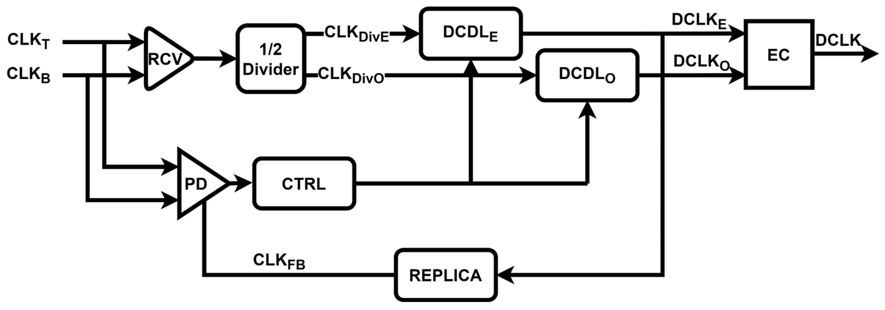
To solve the problem of pulse loss caused by high frequency and narrow clock pulses, the external clock can be divided and then synthesized. Therefore, a single control logic dual delay line DLL (SC-DL DLL) containing a frequency divider was proposed, as shown in Figure 2.
The SC-DL DLL consisted of a receiver (RCV), a frequency divider, a controller (CTRL), two digital control delay lines (DCDLE and DCDLO), a phase detector (PD), a replica module, and an edge combinator (EC). The external input differential clock pair was input to a frequency divider after passing through the receiver to generate a pair of differential clocks CLKDivE and CLKDivO with half the frequency of the external clock. The divided signals were output as DCLKE and DCLKO signals after passing through two delay lines, respectively. The DCLKO signal was phase-detected with the external input clock CLKT after passing through the feedback loop to generate control signals. The DCLKE and DCLKO signals were combined through the combination circuit and then multiplied to obtain the full frequency clock DCLK. If only one delay line was used, the duty cycle of the clock will change after passing through the DCDL, making it impossible for the final generated DCLK to be consistent with CLKT. The purpose of using a dual delay line structure was to use the adjacent rising edges of the output signals of the two delay lines to jointly determine the clock period, so that the synthesized signal was consistent with the external signal and had good jitter performance.
The double delay line jitter analysis of the above DC-DL DLL is shown in Figure 3. The clocks CLKDivE and CLKDivO after external clock splitting were passed through two delay lines, respectively, and generated clocks FBCLKE and FBCLKO after REPLICA module, which were aligned with external clock CLK after DLL locking, respectively. The falling edges of DCLKE and DCLKO cannot be used for clock synthesis due to the duty cycle mismatch of the internal delay module. For this reason, the rising edges of DCLKE and DCLKO need to be used for clock synthesis in the subsequent EC module.
However, in the actual production process, there was a mismatch between the delay lines DCDLE and DCDLO. If only the same control signal was used, the divided clocks FBCLKE and FBCLKO cannot maintain complete consistency after passing through the delay line, resulting in a change in the output clock frequency, duty cycle, or periodic jitter after multiplication.
Since the same code was used to control both delay lines, the mismatch between the two delay lines in practice led to a fixed error in the clock of the second delay line, which was not involved in the phase identification, as shown in Figure 4b, where the purple area was the fixed error from the mismatch of the two delay lines. ΔΦ1 and ΔΦ2 are the duty cycle mismatch present in the delay unit in the DCDL and ΔΦ3 is the mismatch present between the two DCDLs.

3. Principle of DC-DL DLL Structure

3.1. Proposed Structure

The purposed structure is shown in Figure 5. A phase detector was added to the structure shown in Figure 2 for locking the second delay line. Correspondingly, a second controller, CtrlO, was added to generate control signals to control the delay of the delay line DCDLO.
The proposed DC-DL DLL structure shown in Figure 5 was divided into two loops, and the delays of each loop need to satisfy Equation (1). Since the two loops were controlled by two controllers, CTRLE and CTRLO, respectively, the control signals of the two delay lines, DCDLE and DCDLO, can be different. At this time, the two loops satisfied Equations (2) and (3), respectively.
TRCV + Tdiv + Tdly1 + TEC = N × Tck,
TRCV + Tdiv + Tdly2 + TEC = M × Tck,
where TRCV is the delay of receiver, Tdiv is the delay of divider, Tdly is the delay of the delay line, TEC is the delay of EC, Tck is the clock period of the external clock, and N and M are integers. In contrast, the sum of the delay of the replica module and the Muxer in Figure 5 should be equal to TEC. The addition of a second controller, CTRLO, relieves DCDLO from following the delay of DCDLE. Since the mismatch of the dual delay lines can be eliminated by dual-loop locking.
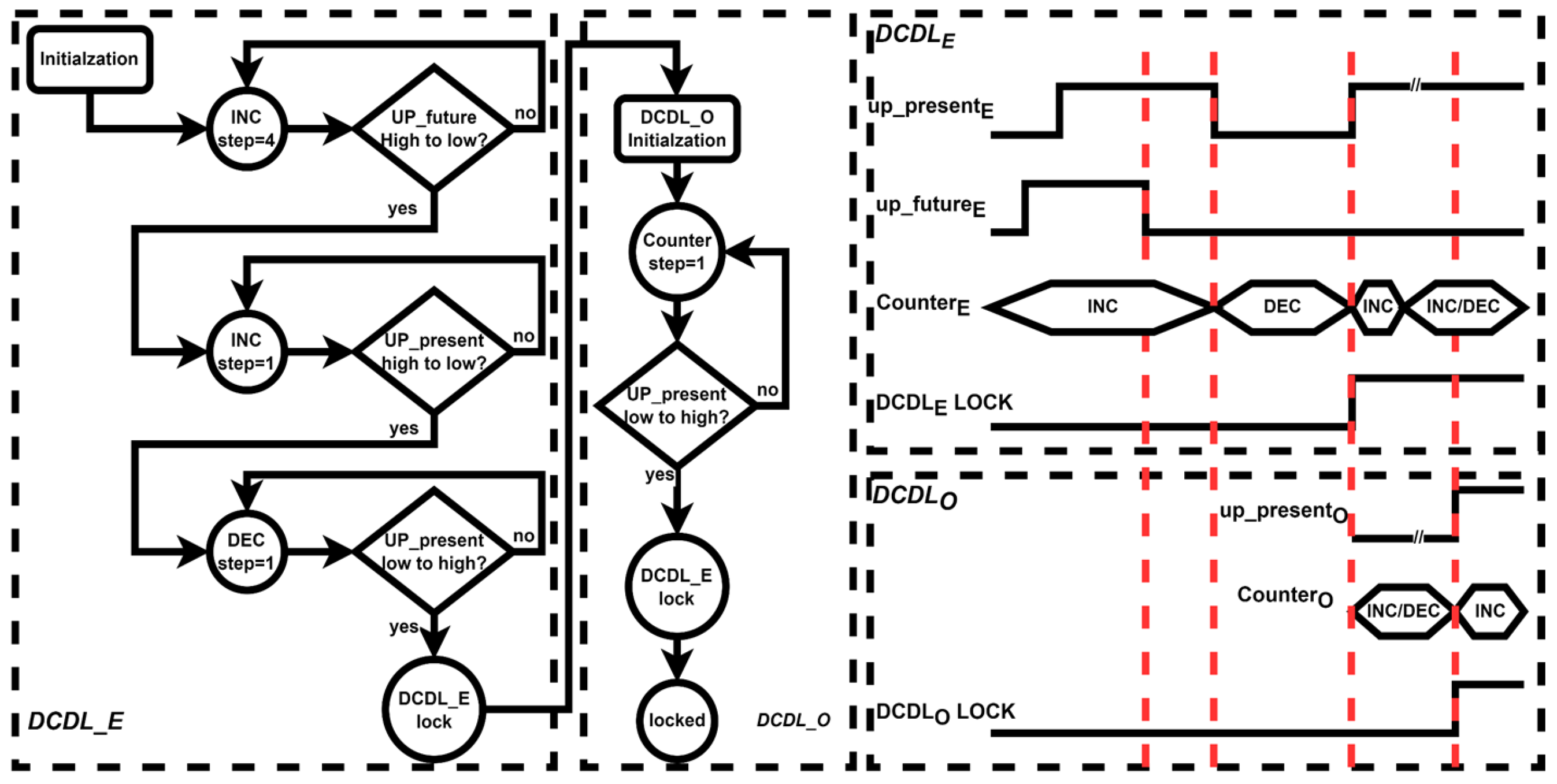
A detailed flowchart of DLL locking is shown in Figure 6. The locking process of the DLL was divided into two parts: the locking process of the delay lines DCDLE and DCDLO. After the DLL was initialized, the counter kept “adding” until the output signal up_present of the bang-bang phase detector flipped from “1” to “0”, and then, the counter became “subtracting” until the up_present signal flipped again. At this point, it was considered that the DCDLE delay line was locked (i.e., the required delay was generated), and then, the digital filter started to work. At the same time, by passing the code of CTRLE at this moment to CTRLO through a latch, the locking of the delay line DCDLO can be accelerated. When an up edge of up_present_O was detected, it was considered that the delay line DCDLO was locked, and currently, it was considered that the entire DLL was locked.
Since, in practice, the delay error between the two delay lines was fixed and was unlikely to cause a large error, it did not take much extra time for the second delay line to lock after transmission through the code.

3.2. Detailed Composition Modules

A block diagram of the phase detector (PD) is presented in Figure 7. Due to the addition of the frequency divider, the clock signal frequency at the input of the phase detector in the current structure was different. Therefore, the bang-bang phase detector structure used can work normally when the input clock frequency was different. The working state of the bang-bang phase detector was divided into “Pre-charge” and “Compare”.
Since the delay of RCV is difficult to replicate, the proposed DLL structure performed phase discrimination on CLKT and CLKFB, but the frequencies of these two signals were different. Therefore, the BBPD used was insensitive to frequency and can work normally when the input clock frequency is different. The bang-bang phase detector had two working states: “Pre-charge” and “Compare”. When CLKFB was “0”, BBPD worked in the pre-charge stage. Points A and B were charged to VDD. MN7 and MN8 were turned on and their drain ends were set to “0”. When CLKFB changed from “0” to “1”, if CLKT > CLKB (CLKFB lags CLKT), the potential at point A was pulled down and through positive feedback, point A was set to “0”, and point B was set to “1”. This stage was the “Compare” stage. The function of PD can be regarded as sampling the CLKT with the CLKFB. When CLKT led CLKFB, up = “1”. When CLKT lagged CLKFB, down = “1”. The function of BBPD can be regarded as sampling the CLKFB for the CLKT. When the CLKT led the CLKFB, up = “1”; when the CLKT lagged the CLKFB, down = “1”.
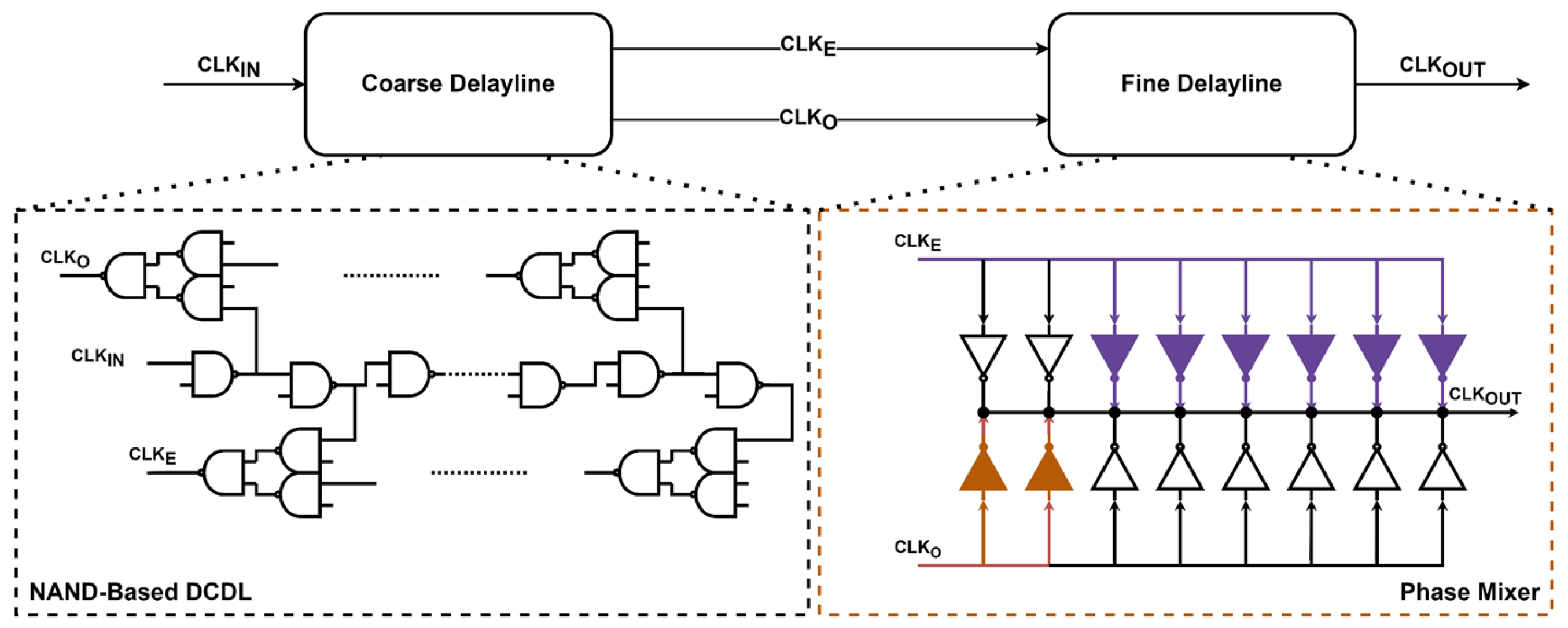
A simple block diagram of the delay line is shown in Figure 8. The coarse adjustment module of the delay line was based on the NAND Cell. By decoding the digital code of the controller, the corresponding NAND logic gate was controlled to switch. The designed coarse delay module was divided into two lines, ODD and EVEN, controlled by five-bit digital signals, respectively. The fine delay module was composed of a phase mixer and interpolated two signals, CLKE and CLKO, with delay, the designed fine delay module was controlled by a sixteen-bit digital signal. Phase mixer type fine delay modules were insensitive to changes in PVT because they work by dividing the delay equally. Its structure was simple and did not require the multi-phase input clock of PRDLL.
Based on the clock timing shown in Figure 4b, the edge combinator (EC) designed in the article was designed to capture the rising edges of DCLKE and DCLKO clocks, as shown in Figure 9. Since only the rising edges of the clocks DCLKE and DCLKO after the delay line DCDL were useful, the proposed EC needed to first perform a frequency division operation on the DCLKE and DCLKO signals to capture their rising edge signals. The rising and falling edges of the generated DCLKM clock corresponded to the rising edges of DCLKE and DCLKO, respectively, and were then combined into a new clock, DCLKM, through a logic gate XOR. After edge synthesis, it was doubled. The periodic jitter introduced by the trigger must be eliminated by adding a delay in the replica module. In addition, traditional frequency doublers were composed of delay units, logic gates, etc., used to multiply the reference frequency. However, the output clock of this structure was easily affected by PVT variables and unregulated supply voltage. The addition of LDO can improve its performance.

4. Results

The proposed DLL chip was designed in the F25 CMOS process. The total power consumption was 10.06 mW from a supply of 1.2 V at 1.6 GHz, with DCDL being the main contributor. The results in this paper were all simulated using the Hspice model provided by the manufacturer, and the simulation software used was Finesim. The accuracy of the transient simulation was 1 ps, and the plots of the results were drawn with Origin2021. The proposed DLL structure can still be locked normally when the duty cycle of the external input clock is only 20%, as shown in Figure 10. The locking of the DLL was not affected by the duty cycle of the external input clock. The duty cycle of the external input clock was reduced by the addition of the frequency divider, which reduced the requirements of the proposed DLL structure.
The simulation results of the current DC-DL DLL with 50% input duty cycle are shown in Figure 11. After single delay line is locked, if the second delay line is not used for re-locking, the output clock DCLK will have a peak-to-peak jitter of about 120 ps due to the mismatch between the delay lines (about 10%). Using the second delay line for locking can effectively eliminate the mismatch between the two DCDLs. Therefore, the peak-to-peak jitter of the final output DCLK clock was reduced to 15.29 ps and its duty cycle was significantly improved and can be maintained between 48.66 and 51.25% after dual delay line is locked. The total locking time of the two delay lines was about 350 TCK, and the time required for locking the second delay line was about 110 TCK.
As the duty cycle of the external input clock was altered from 20% to 80%, it can be observed from the results presented in Figure 12 that the proposed DC-DL DLL was capable of maintaining normal locking functionality, with the duty cycle of the final output clock remaining stable between 48.67% and 51.3%. Upon stabilization of the DLL, the peak-to-peak jitter values of the output clocks corresponding to different duty cycle input clocks were 15.73 ps, 14.69 ps, 14.91 ps, 15.29 ps, 15.87 ps, 17.61 ps, and 16.78 ps, respectively. The simulation results showed that the proposed DC-DL DLL structure had excellent jitter stability in the full input duty cycle range.
Compared with other designs in Table 1, the proposed DC-DL DLL is simple in design and achieves a relatively wide duty cycle input range and is advanced in output duty cycle error.

5. Discussion

A DLL with a wide input duty cycle range was proposed. Compared to the complex design of DCC modules and the high power consumption of TDC, the proposed DC-DL DLL structure is simple in design and does not require additional TDC module design to achieve good duty cycle error in the output clock. The duty cycle range was extended to 20–80% by using a very simple frequency divider structure, whose main constraint was the speed of flip-flop. The proposed EC structure generated the duty cycle error of the signal mainly generated by the frequency multiplier, and so, the LDO was added to improve its performance. Due to the frequency divider and double-loop structure, the proposed DLL had a wide input signal duty cycle range and a small output duty cycle error.

6. Conclusions

In this paper, we presented DC-DL DLL, implemented in the 25 nm CMOS process. This DC-DL DLL design enhanced the noise immunity of the DLL and eliminated concerns regarding mismatches between dual delay lines during the actual production process. The new second delay line required only 100Tck to achieve lock due to the code-transmit setting and achieved a maximum peak to peak jitter of 17.61 ps at 1.6 GHz. The addition of the divider extended the duty cycle range of the external input clock to 20–80%. The maximum output duty cycle error was about 1.3%,with a power consumption of 10.06 mW. The design was straightforward and exhibited superior jitter performance. This architecture can be extensively applied in high-frequency DLL design, and for low-frequency DLLs, the dual delay lines can also improve jitter performance.

Author Contributions

Conceptualization, B.Q.; methodology, B.Q.; software, B.Q. and L.Z.; validation, B.Q. and C.F.; formal analysis, B.Q.; resources, B.Q. and C.F.; data curation, B.Q.; writing—original draft preparation, B.Q.; writing—review and editing, B.Q. and L.Z.; visualization, B.Q.; supervision, P.P.; project administration, P.P.; funding acquisition, P.P. All authors have read and agreed to the published version of the manuscript.

Funding

This research received no external funding.

Data Availability Statement

Data available on request due to restrictions eg privacy or ethical. The data presented in this study are available on request from the corresponding author. The data are not publicly available due to the requirement of company business data confidentiality.

Conflicts of Interest

The authors declare no conflict of interest.

References

  1. Kim, S.Y.; Jin, X.; Chun, J.H.; Kwon, K.W. A Digital DLL with 4-Cycle Lock Time and 1/4 NAND-Delay Accuracy. In Proceedings of the 2015 IEEE Asian Solid-State Circuits Conference (A-SSCC), Xiamen, China, 9–11 November 2015; pp. 1–4. [Google Scholar]
  2. Yang, C.Y.; Li, M.S.; Chuang, A.J. A Wide-Range Folded-Tuned Dual-DLL-Based Clock-Deskewing Circuit for Core-to-Core Links. IEEE Trans. Very Large Scale Integr. Syst. 2021, 29, 883–894. [Google Scholar] [CrossRef]
  3. Zhang, D.; Yang, H.G.; Zhu, W.; Li, W.; Huang, Z.; Li, L.; Li, T. A Multiphase DLL with a Novel Fast-Locking Fine-Code Time-to-Digital Converter. IEEE Trans. Very Large Scale Integr. Syst. 2015, 23, 2680–2684. [Google Scholar] [CrossRef]
  4. Tsai, T.H.; Sheen, R.B.; Hsu, S.Y.; Chang, Y.T.; Chang, C.H.; Staszewski, R.B. A Cascaded PLL (LC-PLL + RO-PLL) with a Programmable Double Realignment Achieving 204fs Integrated Jitter (100 kHz to 100 MHz) and −72 dB Reference Spur. In Proceedings of the 2022 IEEE International Solid-State Circuits Conference (ISSCC), San Francisco, CA, USA, 20–26 February 2022; pp. 1–3. [Google Scholar]
  5. Yang, Z.; Chen, Y.; Yuan, J.; Mak, P.I.; Martins, R.P. A 3.3-GHz Integer N-Type-II Sub-Sampling PLL Using a BFSK-Suppressed Push–Pull SS-PD and a Fast-Locking FLL Achieving −82.2-dBc REF Spur and −255-dB FOM. IEEE Trans. Very Large Scale Integr. Syst. 2022, 30, 238–242. [Google Scholar] [CrossRef]
  6. Qian, Y.C.; Chao, Y.Y.; Liu, S.I. A Low-Jitter Sub-Sampling PLL with a Sub-Sampling DLL. IEEE Trans. Circuits Syst. II Express Briefs 2022, 69, 269–273. [Google Scholar] [CrossRef]
  7. Lu, Y.R.; Liu, S.I.; Yang, Y.C.; Kang, H.C.; Chen, C.L.; Chan, K.U.; Lin, Y.H. A 2.4–3.0 GHz Process-Tolerant Sub-Sampling PLL with Loop Bandwidth Calibration. IEEE Trans. Circuits Syst. II Express Briefs 2021, 68, 873–877. [Google Scholar]
  8. Park, D.; Kim, J. A 7-GHz Fast-Lock 2-Step TDC-based All-Digital DLL for Post-DDR4 SDRAMs. In Proceedings of the 2018 IEEE International Symposium on Circuits and Systems (ISCAS), Florence, Italy, 27–30 May 2018; pp. 1–4. [Google Scholar]
  9. Kim, T.; Kim, J. A 0.8–3.5 GHz Shared TDC-Based Fast-Lock All-Digital DLL with a Built-in DCC. In Proceedings of the 2021 IEEE International Symposium on Circuits and Systems (ISCAS), Daegu, Republic of Korea, 22–28 May 2021; pp. 1–4. [Google Scholar]
  10. Jung, D.H.; An, Y.J.; Ryu, K. All-digital fast-locking delay-locked loop using a cyclic-locking loop for DRAM. IEEE Trans. Circuits Syst. II Express Briefs 2015, 62, 1023–1027. [Google Scholar] [CrossRef]
  11. Na, T.; Shim, Y.; Song, I.; Kim, J.K. A Heterogeneous Dual DLL and Quantization Error Minimized ZQ Calibration for 30 nm 1.2 V 4 Gb 3.2 Gb/s/pin DDR4 SDRAM. In Proceedings of the 2013 Symposium on VLSI Circuits, Kyoto, Japan, 12–14 June 2013; pp. C242–C243. [Google Scholar]
  12. Tsai, C.W.; Chiu, Y.T. A Wide-Range All-Digital Delay-Locked Loop for DDR1–DDR5 Applications. IEEE Trans. Very Large Scale Integr. Syst. 2021, 29, 1720–1729. [Google Scholar] [CrossRef]
  13. Kim, D.; Park, M. A 1.1-V 10-nm Class 6.4-Gb/s/Pin 16-Gb DDR5 SDRAM With a Phase Rotator-ILO DLL, High-Speed SerDes, and DFE/FFE Equalization Scheme for Rx/Tx. IEEE J. Solid-State Circuits 2020, 55, 167–177. [Google Scholar] [CrossRef]
  14. Park, H.; Sim, J. A 2.4–8 GHz Phase Rotator Delay-Locked Loop Using Cascading Structure for Direct Input–Output Phase Detection. IEEE Trans. Circuits Syst. II Express Briefs 2022, 69, 794–798. [Google Scholar] [CrossRef]
  15. Yun, W.J.; Song, I.; Jeoung, H. 17.7 A Digital DLL with Hybrid DCC Using 2-Step Duty Error Extraction and 180° Phase Aligner for 2.67 Gb/S/pin 16 Gb 4-H Stack DDR4 SDRAM with TSVs. In Proceedings of the 2015 IEEE International Solid-State Circuits Conference-(ISSCC) Digest of Technical Papers, San Francisco, CA, USA, 22–26 February 2015; pp. 1–3. [Google Scholar]
  16. Yoon, H.; Jung, W.; Park, J.; Byun, J.; Jin, H.; Cho, H.; Lee, S.H. A 3.2–12.8 Gb/s Duty-Cycle Compensating Quadrature Error Corrector for DRAM Interfaces, with Fast Locking and Low Power Characteristics. In Proceedings of the ESSCIRC 2021-IEEE 47th European Solid State Circuits Conference (ESSCIRC), Grenoble, France, 13–22 September 2021; pp. 463–466. [Google Scholar]
  17. SR, J.P.; Hiremath, S.S. Dual Loop Clock Duty Cycle Corrector for High Speed Serial Interface. In Proceedings of the 2017 International Conference on Smart Technologies for Smart Nation (SmartTechCon), Bengaluru, India, 17–19 August 2017; pp. 935–939. [Google Scholar]
  18. Jeong, C.H.; Abdullah, A.; Min, Y.J.; Hwang, I.C.; Kim, S.W. All-digital duty-cycle corrector with a wide duty correction range for DRAM applications. IEEE Trans. Very Large Scale Integr. Syst. 2015, 24, 363–367. [Google Scholar] [CrossRef]
  19. Ryu, K.; Jung, D.H.; Jung, S.O. Process-variation-calibrated multiphase delay locked loop with a loop-embedded duty cycle corrector. IEEE Trans. Circuits Syst. II Express Briefs 2013, 61, 6678577. [Google Scholar] [CrossRef]
  20. Chae, J.H.; Ko, H.; Park, J.; Kim, S. A quadrature clock corrector for DRAM interfaces, with a duty-cycle and quadrature phase detector based on a relaxation oscillator. IEEE Trans. Very Large Scale Integr. Syst. 2019, 27, 978–982. [Google Scholar] [CrossRef]
  21. Lim, J.H.; Bae, J.H. A Delay Locked Loop with a Feedback Edge Combiner of Duty-Cycle Corrector With a 20–80% Input Duty Cycle for SDRAMs. IEEE Trans. Circuits Syst. II Express Briefs 2016, 63, 141–145. [Google Scholar] [CrossRef]
  22. Sim, J.; Park, H. A 1–3.2 GHz 0.6 mW/GHz Duty-Cycle-Corrector Using Bangbang Duty-Cyle-Detector. In Proceedings of the 2021 IEEE International Symposium on Circuits and Systems (ISCAS), Daegu, Republic of Korea, 22–28 May 2021; pp. 1–4. [Google Scholar]
  23. Kang, K.T.; Kim, S.Y.; Kim, S.J.; Lee, D.; Yoo, S.S.; Lee, K.Y. A 0.33–1 Ghz open-loop duty cycle corrector with digital falling edge modulator. IEEE Trans. Circuits Syst. II: Express Briefs 2018, 65, 1949–1953. [Google Scholar] [CrossRef]
  24. Chung, C.C.; Sheng, D.; Li, C.J. A wide-range low-cost all-digital duty-cycle corrector. IEEE Trans. Very Large Scale Integr. Syst. 2014, 23, 2487–2496. [Google Scholar] [CrossRef]
Figure 1. Traditional feedback-based DLL structure.
Electronics 12 02696 g001
Figure 2. SC-DL DLL structure.
Electronics 12 02696 g002
Figure 3. (a) Output clock of single delay line structure; (b) output clock of dual delay line.
Electronics 12 02696 g003
Figure 4. (a) Output clock of dual delay line in ideal situation; (b) output clock of dual delay line in actual situation.
Electronics 12 02696 g004
Figure 5. Purposed DC-DL DLL structure.
Electronics 12 02696 g005
Figure 6. Flowchart of DLL locking.
Electronics 12 02696 g006
Figure 7. Bang-Bang Phase Detector.
Electronics 12 02696 g007
Figure 8. The delay line of purposed DLL structure.
Electronics 12 02696 g008
Figure 9. Edge combinator.
Electronics 12 02696 g009
Figure 10. Locking with 20% duty cycle external clock signal.
Electronics 12 02696 g010
Figure 11. Proposed DC-DL DLL Performance Simulation: (a) Locking with 50% duty cycle external clock signal; (b) Jitter after single delay line lock; (c) Jitter after dual delay line lock; (d) Duty cycle after single delay line lock; (e) Duty cycle after dual delay line lock.
Electronics 12 02696 g011
Figure 12. Edge combinator.
Electronics 12 02696 g012
Table 1. Comparison with previous works.
This WorkVLSI [3]IEEE T CIRCUITS-II [6]ISCAS [22]
ArchitectureDivider + Dual delay lineADDLLDivider + DCCBBDCD
Supply Voltage1.2 V1 V1.2 V1 V
Input Frequency Range1.6 GHz0.1–2.7 GHz1.6 GHz/2 GHz1–3.2 GHz
Input Clock Duty Cycle Range20–80%N/A19.9–80.4%37–63%
MAX Duty Cycle Error1.3%1.9%0.9%1.5%
RMS/Peak to Peak Jitter−/17.61 ps0.65 ps/5 ps2.7 ps/14 ps−/12 ps
AREAN/A0.089 mm20.099 mm20.001 mm2
Power@Fmax10.06 mW49.4 mW6.6 mW1.92 mW
Technology25 nm90 nm65 nm28 nm
Disclaimer/Publisher’s Note: The statements, opinions and data contained in all publications are solely those of the individual author(s) and contributor(s) and not of MDPI and/or the editor(s). MDPI and/or the editor(s) disclaim responsibility for any injury to people or property resulting from any ideas, methods, instructions or products referred to in the content.