Article

Benefits from Using Very Thin Channel Layer for TFTs

by
Mamadou Lamine Samb
1,2,*,
Emmanuel Jacques
1,
Amadou Seidou Maiga
3,* and
Tayeb Mohammed-Brahim
1
1
OASIS-IETR, UMR CNRS 6164, Bat.11B, Campus de Beaulieu, Université de Rennes, 35042 Rennes, France
2
ED2DS, University Iba Der Thiam, BP 1039, Thies 99341, Senegal
3
LEITER, University Gaston Berger, BP 234, Nationale 2, Route de Ngallele, Saint-Louis 99341, Senegal
*
Authors to whom correspondence should be addressed.
Electronics 2023, 12(12), 2694; https://doi.org/10.3390/electronics12122694
Submission received: 8 February 2023 / Revised: 22 March 2023 / Accepted: 17 April 2023 / Published: 16 June 2023

Abstract

:
It is known from many published data on amorphous or polycrystalline silicon and on metal oxides based Thin Film Transistors (TFTs) that their electrical parameters improve when decreasing the thickness of the channel layer. The origin of this improvement is discussed here through electrostatic arguments only. In particular, it is shown that the behavior of the subthreshold swing with the thickness does not depend on the type of materials. The material and its electrical defects determine only the importance of the improvement but not the trend towards better electrical parameters. Meanwhile, in general, the electrical stability under gate stress enhances too. The improved stability is explained by the reduced electronic charge inside the channel layer, leading to a lower injection of electrons in the gate insulator.

1. Introduction

A Thin Film Transistor (TFT) is a stack of insulator and semiconductor thin films. The channel layer of these transistors is a thin semiconductor film that is deposited at low temperature. The electrical quality of this film has a direct consequence on the performance of the TFT. When a semiconducting film is directly deposited, it is not single crystalline. It can be amorphous or nano-micro-poly crystalline depending on the technique used and the deposition conditions. Such a non-single crystalline structure leads to the presence of numerous permitted energy states for electrons in the energy forbidden bandgap. The electrical conduction of the film is lowered in consequence. Remarkable efforts are made to improve the quality of the material. However, whatever the improvements, it will not remain a single crystalline and will still contain electrically active defects. Considering this limit in the improvement of the electrical quality of the material, we need to explore other ways to improve the electrical parameters of the transistor. As described in this report, such a way consists of decreasing the thickness of the channel layer, mimicking what has already been performed in old works on SOI FETs [1,2,3,4]. Indeed, in both TFTs and SOI-FETs, the interfaces between the channel layer and the gate insulator, as well as between the channel layer and the substrate, are so close that they induce a potential interaction in-between.
In fact, improving the transistor’s parameters by decreasing the thickness of the channel layer is not specific to SOI FETs but seems a universal rule, as observed in other transistors based on different materials (Polysilicon [5,6], hydrogenated amorphous silicon [7], different metal-oxides, such as InZnO [8], InGaZnO [9], InSnZnO [10], and InGaSnO [11]).
In this work, after demonstrating the effect of the channel layer’s thickness through the example of as-deposited crystalline (or micro-poly crystalline) silicon based TFTs, the improvement is explained by means of electrostatic arguments only, independent of the type of material.
Moreover, we show that the electrical stability of the TFTs’ electrical characteristics when these transistors are submitted to high gate voltage is improved when the thickness of the channel diminishes. This improvement occurs under the condition in which the physical structure of the channel material does not alter during the application of the gate voltage, meaning that no electrically active defect is created during the process.

2. As-Deposited Micro-Poly Crystalline Silicon Based TFTs as an Example of the Effect of Channel Layer Thickness Variation

2.1. Process

As-deposited micro-poly crystalline silicon films, deposited at 165 °C by PECVD using highly diluted in hydrogen–argon silane, are used as the channel layer and doped source, and the drain contacts. The structure of as-deposited crystalline silicon is micro-poly crystalline. It was previously shown [12] that adding argon in the usual silane–hydrogen mixture leads to good improvement in the crystalline volume in the silicon film. For example, the addition of argon allows the crystalline volume to increase from 24% to 58% for 20 nm thick films. Arsine is added to the previous gas mixture during the deposition of the doped silicon film. A high electrical conductivity of the doped silicon layer is obtained when using arsenic as a dopant. Its value is 5 S/cm at normal temperature.
After the successive deposition of an undoped channel layer and a doped layer, this last layer is SF6 plasma etched to define the source and drain regions. Then, silicon nitride film with a thickness of 300 nm is deposited at 150 °C by PECVD. It will act as a gate insulator. After SF6 plasma etching of the insulating layer, an aluminum layer is deposited and etched to form a source, a gate and a drain contacts. Post-metallization annealing is performed at 180 °C in an atmosphere of forming gas. The maximum temperature used in the process is 180 °C. It is reached during the last step of the process. The process leads to the TFT structure shown in Figure 1. More details on the process can be found in [13].

2.2. Electrical Characterisation of TFTs Having a Channel Layer with a Different Thickness

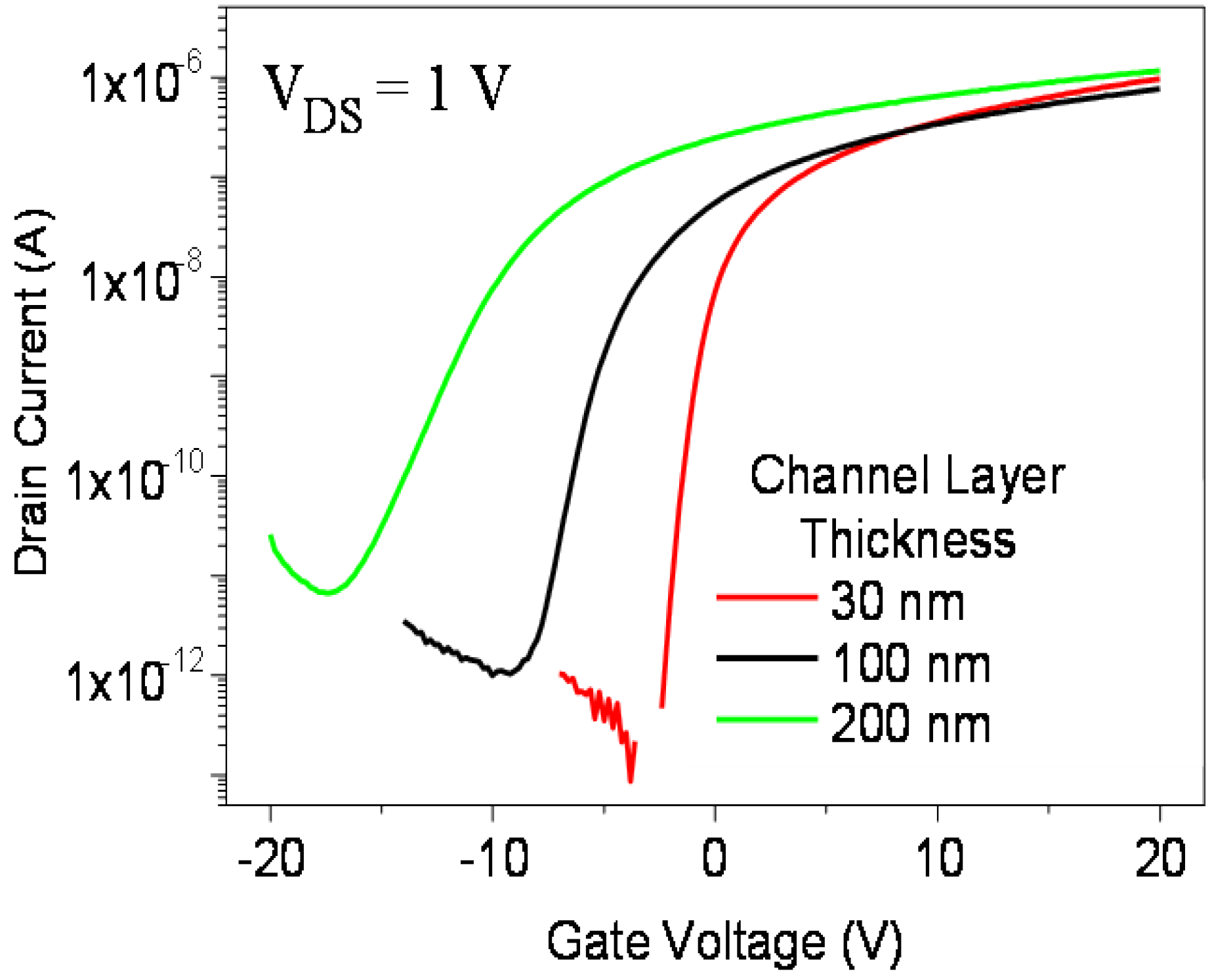
The transfer characteristics of n-type TFTs using a 200 nm, 100 nm or 30 nm thick channel layer are shown in Figure 2. The transfer characteristics are the drain current versus gate voltage at fixed drain voltage curves. Here, the drain voltage was set at +1 V, meaning the transistors work in the linear mode. The behavior of the curves as a function of the channel layer thickness is similar to what we found previously [14], meaning a shift of the characteristics towards negative voltage values and an increase in the subthreshold swing when the channel layer is thicker.
Table 1 provides the electrical parameters of these three different channel layer thickness TFTs, deduced from the transfer’s characteristics.
The electrical parameters, mobility µ, subthreshold swing SS, threshold voltage VTH and the ratio ION/IOFF, are deduced following their usual definitions in the linear mode.
µ is calculated in the linear mode using the usual equation of the transconductance gm of a MOSFET:
μ = g m L W 1 C i n s 1 V D S
L and W are the length and the width of the channel, respectively. Cins is the capacitance per area unit of the gate insulator. VDS is the applied drain–source voltage. gm is the maximum slope of the linear plot of the drain current versus the gate voltage curve.
The linear extrapolation on the gate voltage axis of this last curve provides the threshold voltage.
The inverse of the maximum slope of the drain current versus the gate voltage curve plotted in a semi-logarithmic scheme provides the subthreshold swing SS.
At a higher channel layer thickness, the mobility is higher, and the subthreshold swing is higher as well, while the threshold voltage is lower. This general trend is similar to what we can find in many papers on TFTs made with so many different materials, such as Thermally oxidized polysilicon [5] or Solid-Phase Crystallized (SPC) polysilicon [6], amorphous silicon [7], InZnO [8], Inkjet-printed InGaZnO [9], InSnZnO [10], and InGaSnO [11].
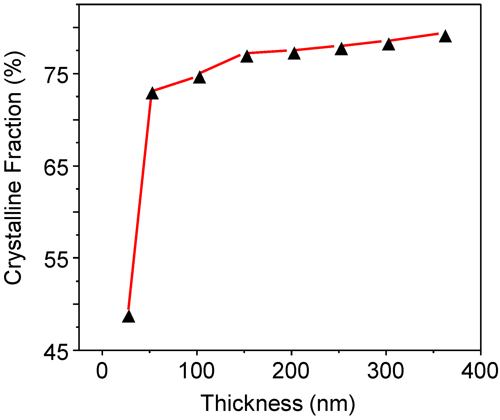
The shift of the threshold voltage towards negative values can be explained by the different crystalline quality of as-deposited micro-poly crystalline silicon films with different thicknesses. Indeed, the crystalline fraction of as-deposited micro-poly crystalline silicon films increases continuously from 0 to a thickness of 50 nm. It saturates at 77% for higher thicknesses (Figure 3) [15]. We can assume that the electrical quality increases along with an increase in the crystalline fraction. The increase in electron mobility with the thickness supports such an assumption. The free electron accumulation under the insulator (in the channel) when the gate voltage increases becomes easier when the thickness becomes higher, inducing, then, a decrease in the threshold voltage. Even if this explanation is true, it cannot explain by itself the larger difference between the threshold voltage of 100 nm and 200 nm thick channel layers as well as between 30 nm and 100 nm thick layers. Indeed, the crystalline fraction jumps from 50% for 30 nm thick layer to 75% for a 100 nm thick layer; although it varies only from 75% to 77% for 100 nm to 200 nm layers.
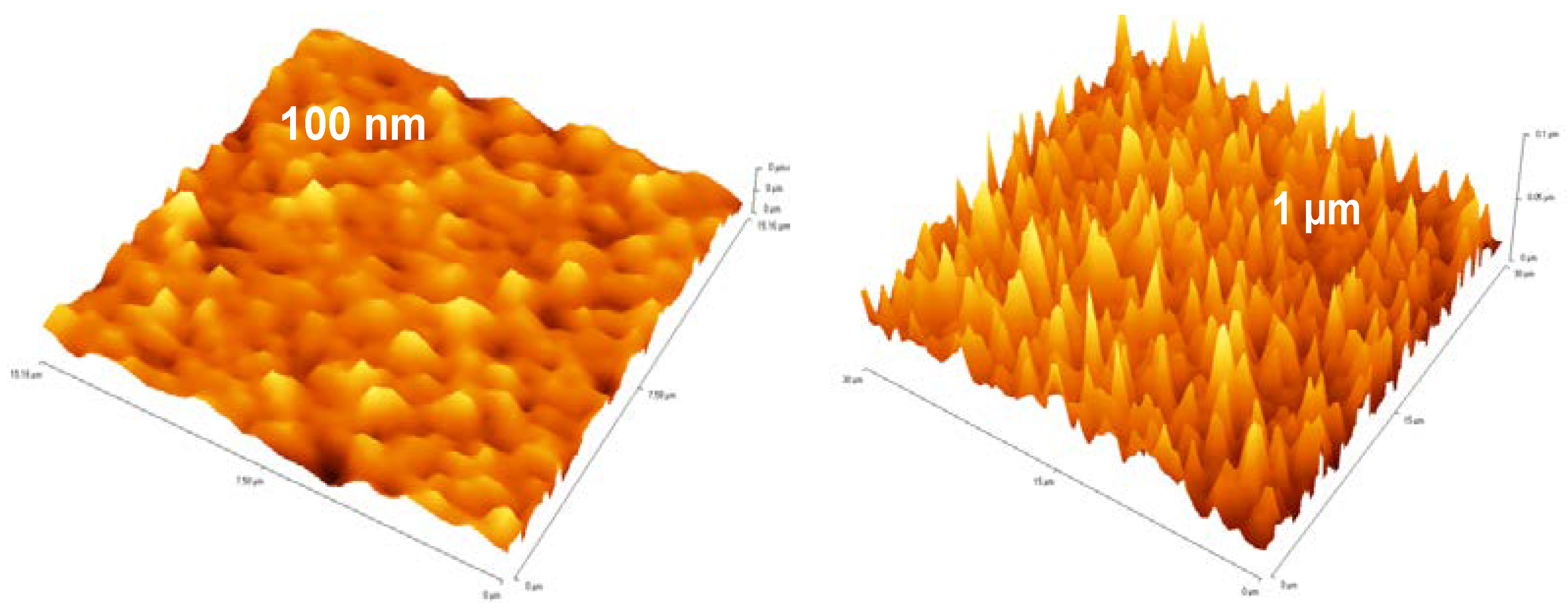
An explanation of the increase in the subthreshold swing when the thickness increases may invoke the increase in the surface roughness of the channel layer. A higher roughness induces electrically active defects at the interface between the channel layer and the gate insulator leading to an increase in the swing. Figure 4 shows the images of the surface of 100 nm thick and 1 µm thick microcrystalline silicon layers, taken by Atomic Force Microscope (AFM). The surface RMS roughness increases from 0.6 nm to 12 nm. Such an increase may explain the increase in the subthreshold swing.
Even if previous explanations of the shift in the threshold voltage along with the change in the swing may be applied, at least to some extent, to the case of present as-deposited crystalline silicon TFTs, their extension to TFTs or MOSFETs based on many other materials is questionable. The crystalline quality and the roughness of single crystalline silicon do not change with the layer’s thickness.
The correct explanation cannot involve the type of material as the behavior is general. Whatever the material, the threshold voltage and the subthreshold swing decrease when the thickness of the channel layer decreases.
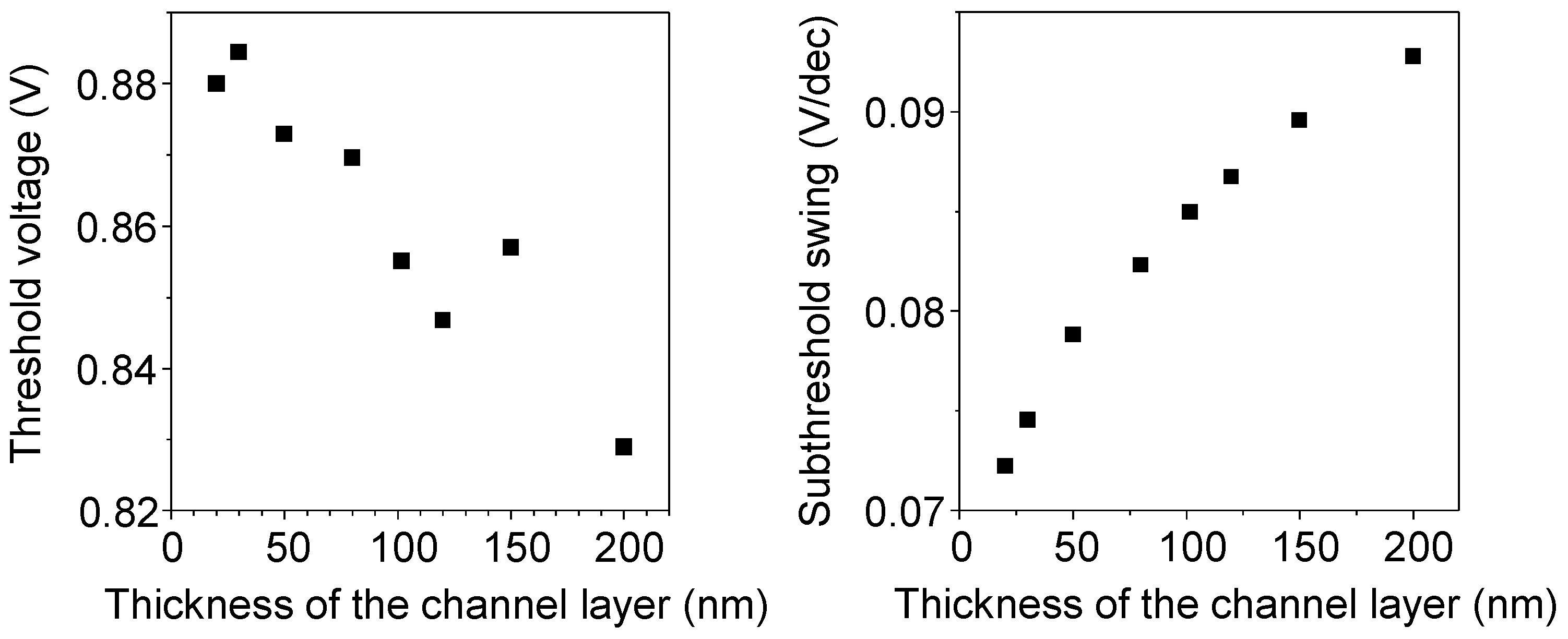
Previously [16], by using a model based on Silvaco software tools, particularly Athena [17] and Atlas [18], we showed the same behavior of the threshold voltage and subthreshold swing as a function of the thickness of the channel layer using only electrostatic arguments. Figure 5 shows these behaviors, as given by this model, for single crystalline silicon based TFTs.
The same behaviors were found in a simulation of SOI-MOSFETs [4], considering a high thick back insulator as a substrate and a weakly doped silicon channel layer. These conditions are fulfilled in the present case of as-deposited silicon TFTs using glass as a substrate and un-doped silicon as a channel layer.
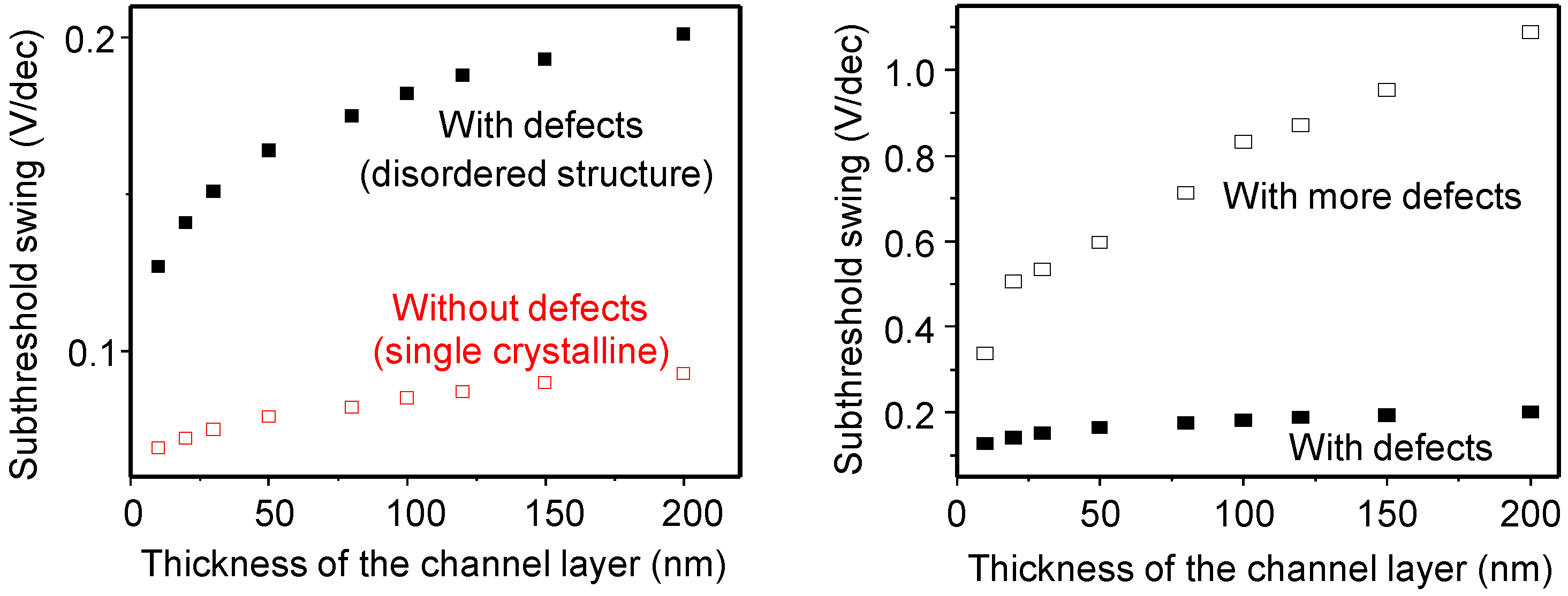
If we consider a silicon channel with a disordered structure, containing electrically active defects (distribution of energy states in the forbidden gap), the same behavior of the subthreshold swing is found (Figure 6). The subthreshold swing decreases when the thickness of the channel layer decreases.
Figure 6 shows that the variation is much more important when the material contains a high content of defects. Thus, as known for single crystalline silicon MOS-FETs or SOI-FETs, the decrease in the channel layer’s thickness is advantageous for the subthreshold swing. The present study shows the higher benefit when doing the same for disordered material based transistors. The more the material is defected, the more the reduction in the channel layer thickness is beneficial. The effect of the decrease in the channel layer thickness is more spectacular for the defected material-based TFTs.
This benefit can only be explained by the more and more important role of the lateral electrical field (between the source and the channel) when the thickness decreases.
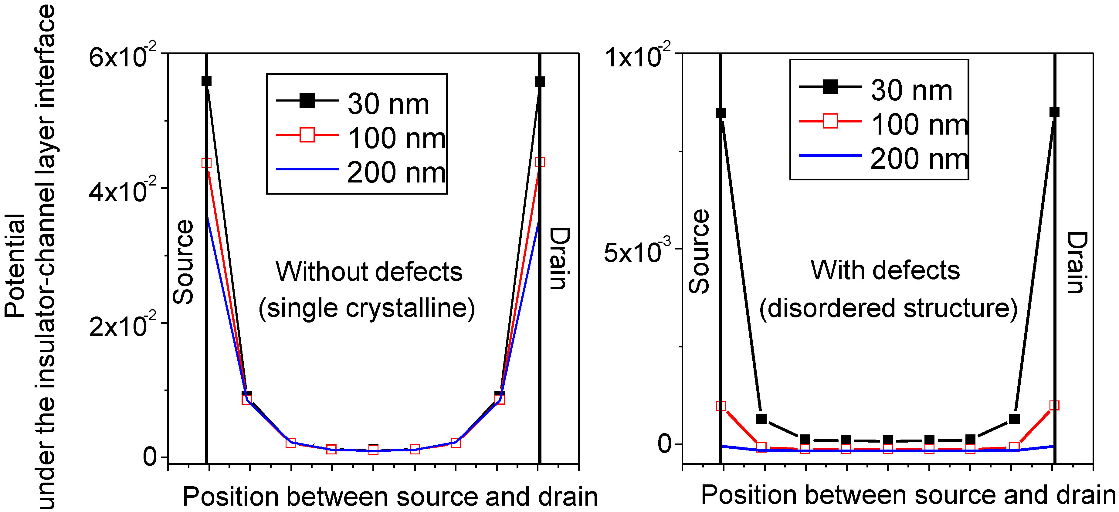
The lateral electrical field is shown in Figure 7 through the profile of the potential. This potential is calculated just under the insulator–channel layer interface along the channel between the source and the drain.
The variation of the potential is much more important close to the source–channel layer and drain–channel layer interfaces, meaning a more important field effect at these interfaces. At these interfaces, the variation of the potential is more important when the thickness of the channel layer decreases for both single and disordered materials. For single crystalline materials, the variation is important whatever the channel’s thickness. In the case of a disordered material, the profile of the potential is nearly flat, meaning no field, with a thickness of 200 nm. It increases near the interfaces, a little bit with a 100 nm thickness and frankly (by a factor of 104) with a 30 nm thickness. Comparatively, the potential at the source–channel interface increases by a factor of four only in the case of single crystalline. This means that the electrical field between the source and the channel layer becomes very important only with a 30 nm thick channel layer in the case of disordered material. At higher thickness, it is screened by the defects.
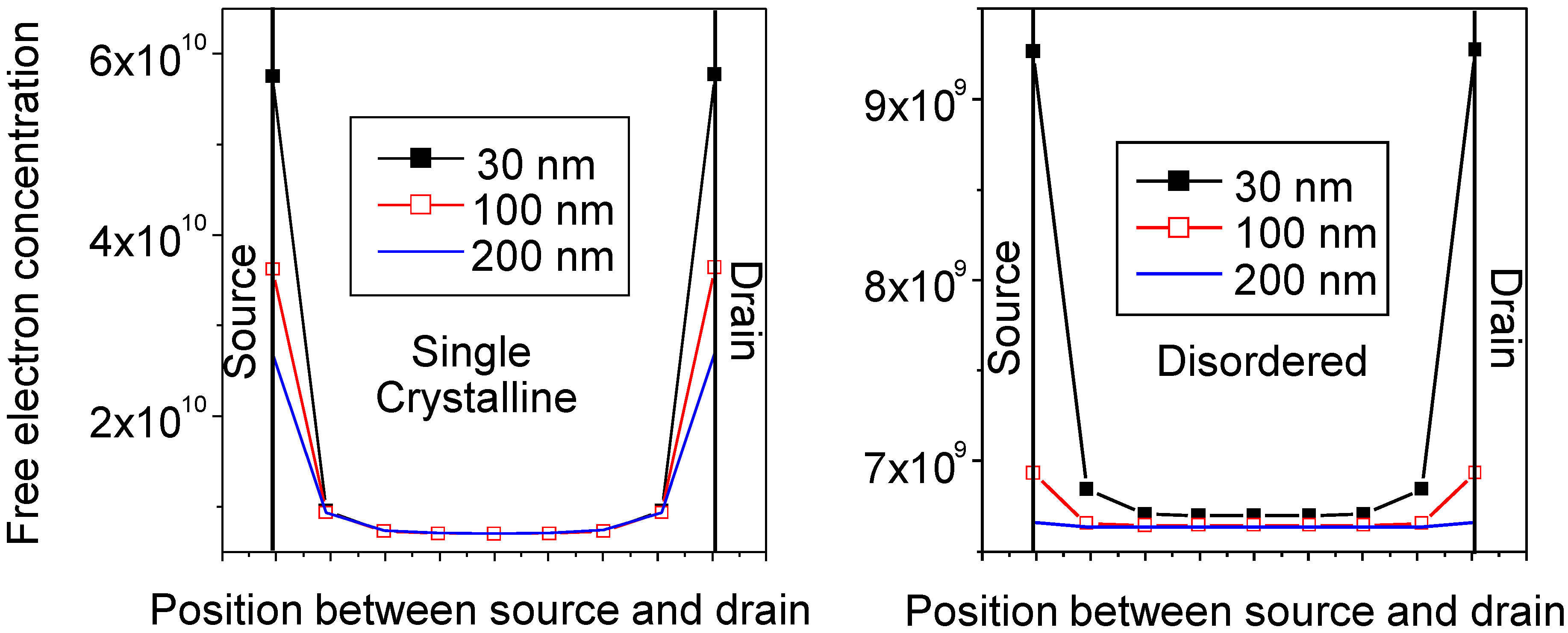
The behavior of the free electron concentration between the source and drain (Figure 8) follows that of the potential. In a single crystalline channel, whatever its thickness, free electrons are present in the channel near the source and the drain even if no voltage is applied. In a disordered channel, free electrons are present near the source and the drain only at a very low channel thickness. Nearly no free electrons are present when the channel’s thickness is high. This profile shows how the channel forms with ease in a single crystalline material whatever the thickness. The channel’s formation is easier when the thickness decreases. In a disordered material, the channel’s formation is very difficult when the thickness is high. It becomes easy only at thicknesses lower than 30 nm.
In conclusion, the similar trend of the threshold voltage and of the subthreshold swing with the thickness of the channel’s layer, whatever the type of material, may only be explained by electrostatic arguments. Involving the specific properties of the material is not needed to clarify the behavior. A specific material may only need to be involved to explain the more or less important variation.

3. Electrical Stability of Thin Channel Layer-Based TFTs

After explaining the behavior of the TFT’s electrical parameters as a function of the channel’s thickness, we focus now on their electrical stability. Generally, if the semiconducting material stays uniform when changing its thickness, TFTs with a thinner channel layer seem more stable under gate bias stress [19]. Here, we will try to confirm this trend through the example of previous as-deposited crystalline silicon-based TFTs.
First, we check the stability of an as-deposited crystalline silicon TFT using only one channel layer thickness, i.e., 100 nm. We will try to explain the possible shift of the transfer characteristics when a high gate bias is applied. Secondly, this explanation will help us to understand the possible variation of the shift when using different channel thicknesses.

3.1. Electrical Stability of TFTs with a 100 nm Thick Channel Layer

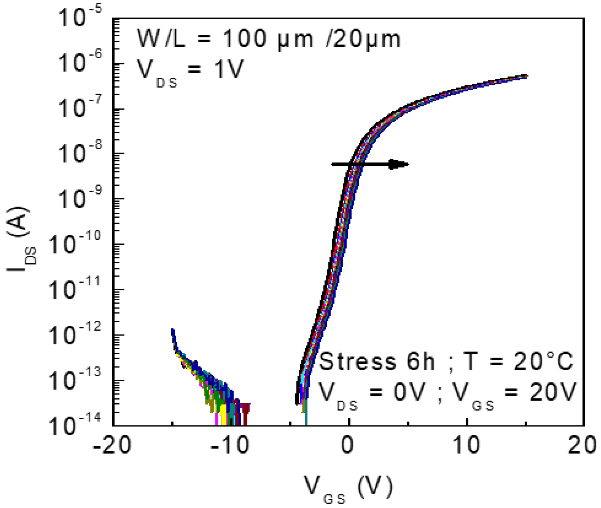
During electrical stress, the source and drain are short-circuited while a positive gate voltage is applied for a few hours. The stress is stopped at some time intervals for the purpose of plotting the transfer characteristics. Figure 9 shows the transfer characteristics of TFTs submitted to a gate voltage stress of +20 V at normal temperature (fixed at 20 °C). The total duration of the stress is 6 h. The time between the two transfer characteristics is 10 min.
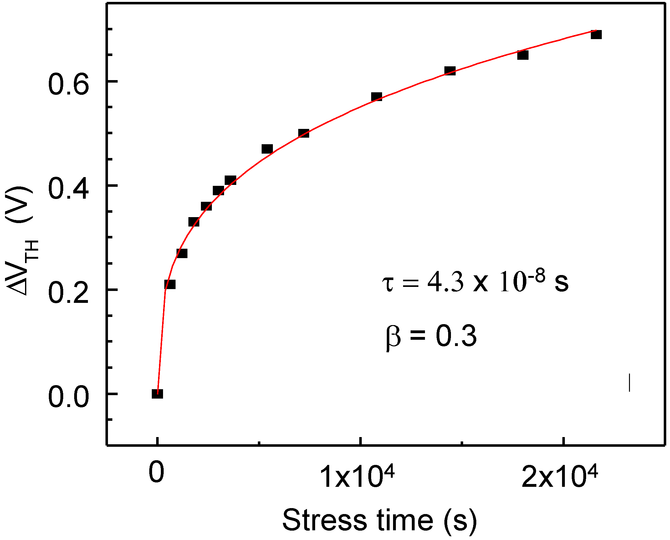
Firstly, the transfer characteristics shift towards a positive gate voltage under stress with no change in the subthreshold swing. The positive shift is very weak. The total shift after 6 h is 0.7 V. The shift is quantified by plotting the variation of the threshold voltage ΔVTH = VTH(t) − VTH0 as a function of the stress time t. The ΔVTH(t) curve and its fit by a stretched exponential function are plotted in Figure 10.
The stretched exponential function [20] is given by:
V T = ( V G V T H 0 ) 1 e x p t τ β
where VTH0 is the initial threshold voltage and t is the stress time. β et τ are two parameters that provide the kinetics of the variation.
As described in Ref. [21], this function is a law that explains the relaxation phenomena in glasses towards some equilibrium state after the application of some constraint. It was established by considering particles that may diffuse in a medium with some spatially random distributed states able to capture them [21]. It was used in disordered structures to describe the time behavior of some parameters, such as the conductivity [22], threshold voltage of the TFTs [23], and the magnetization [20]. It was linked in amorphous silicon-based TFTs to the dispersive diffusion coefficient of hydrogen atoms [23]. The dispersion comes from the nature of a disordered medium where the trapping sites show a distribution of the energy states available. The β parameter depends on this distribution and on the temperature.
As this stretched exponential law is general enough, describing the effect of a stress in various cases, such as in glasses, in MOFET’s transistors [24], and in un-hydrogenated polycrystalline silicon TFTs where the diffusion of hydrogen atoms cannot be involved, could be linked to the disorder that is present in amorphous materials or in crystalline materials through the disordered regions at the interfaces or the grain boundaries.
We may assume that, inside these disordered regions where the bonds are weak, the accumulation of electrical charges or the presence of local high electrical fields induce a change in the constraint state and, particularly, a change in the states of the weakest bonds. The deformation may diffuse, establishing a new equilibrium, characterized by a new state distribution.
The disordered structures provide some flexibility for a rearrangement of the bonds in the material. More generally, the equilibrium of a disordered structure comes from the electrical charges and states. When these distributions are disrupted, as in the case of a charge accumulation in TFTs, the structure tends towards a new equilibrium.
The values of the parameters β et τ, providing the kinetics of the variation of the TFT’s characteristics, are deduced from the previous fit of the variation of the threshold voltage (Figure 7).
β = 0.3     τ = 4.3 × 10⁸ s
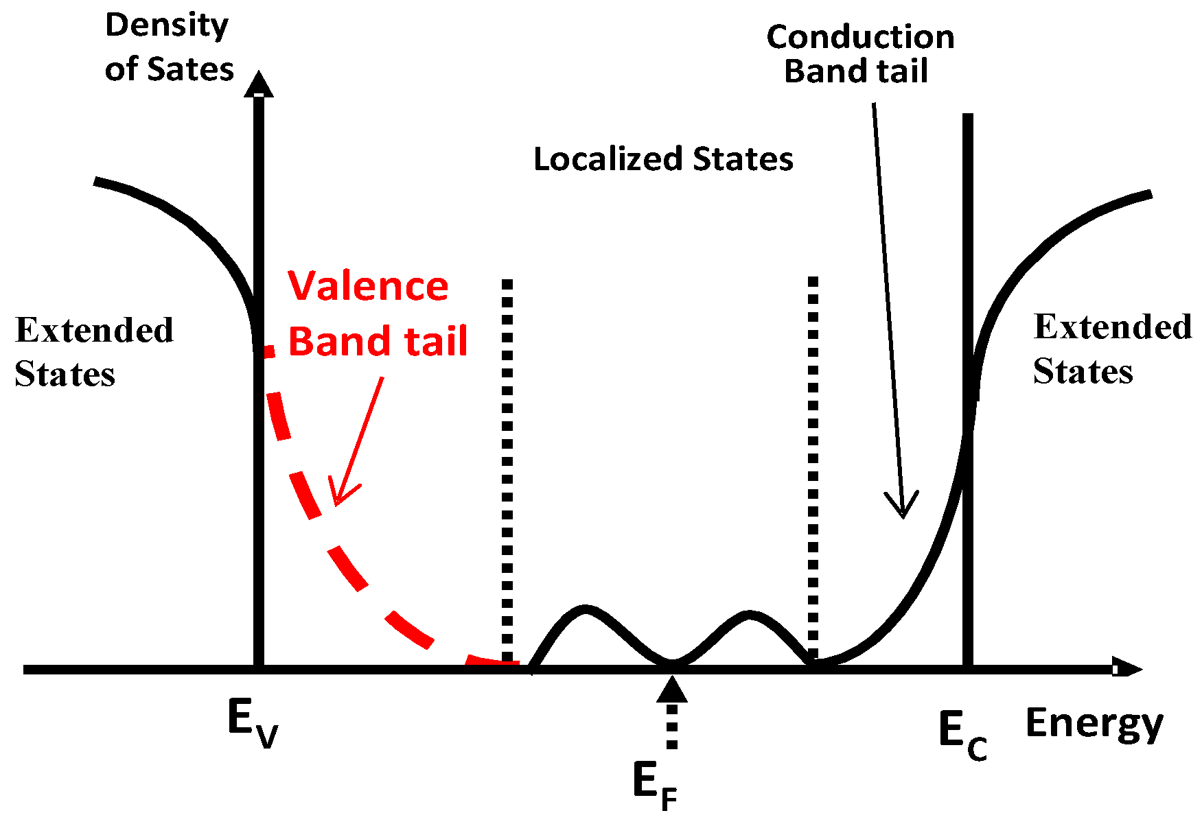
The β value seems very weak. β is related to the Urbach energy that is provided by the slope of the exponential of the energy states’ density in the valence band tail in any disordered material (Figure 11).
β is given by the simple ratio: β = kT/kT0
where kT0 is the Urbach energy. Taking the above value of β, the Urbach energy of the present as-deposited crystalline silicon used as a channel layer is 84 meV. This value is much too high, particularly for the present crystalline silicon, which has a crystalline fraction as high as 75% (Figure 3).
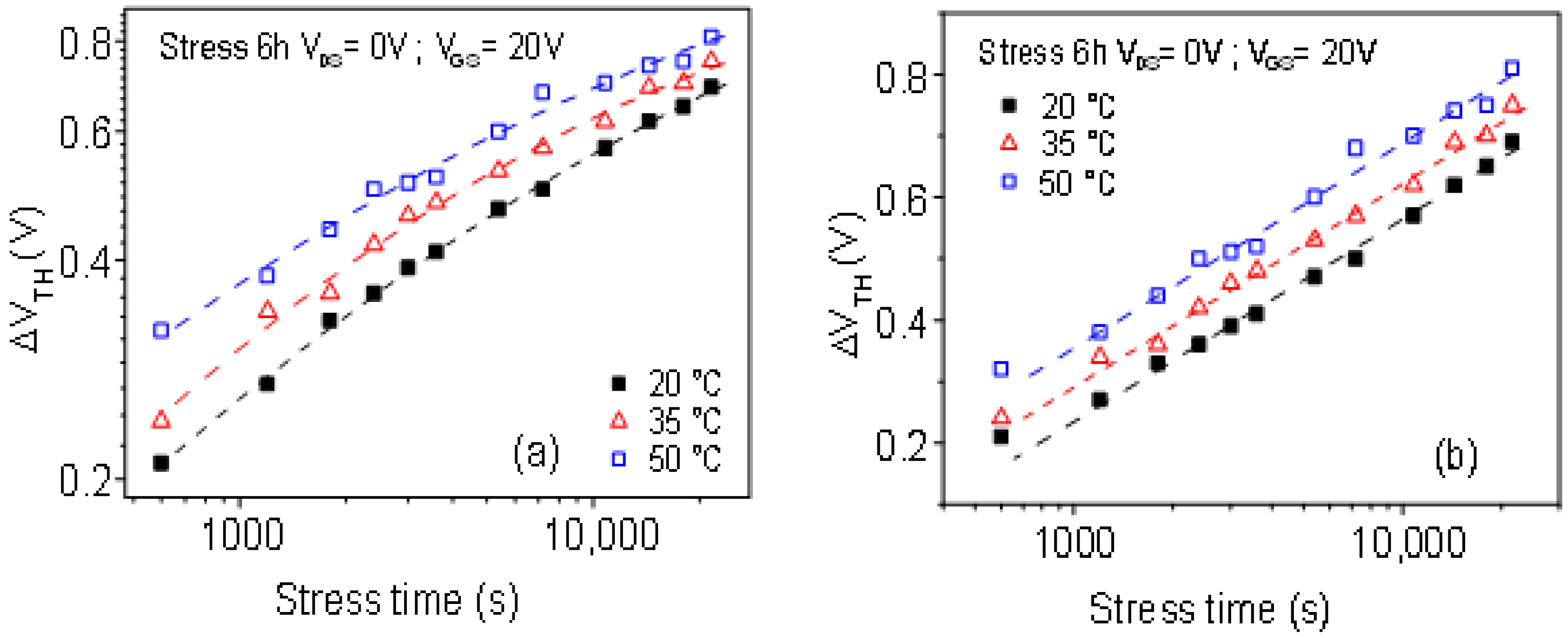
To check on the origin of this weak value of β, one way is to plot the variation ΔVTH using a logarithmic graph (log(ΔVTH) − log(t)) or semi-logarithmic graph (ΔVTH − log(t)). Indeed, the variation ΔVTH coming from charge trapping inside the gate insulator follows semi-logarithmic law [20], whereas defect creation inside the channel follows logarithmic law [25,26]. The logarithmic law is only the beginning of the stretched exponential function at low time values. The variation in the threshold voltage under the application of +20 V gate voltage for 6 h at 20 °C, 35 °C and 50 °C is plotted in Figure 12a,b using a logarithmic or semi-logarithmic graph, respectively. It appears that the curves plotted using a semi-logarithmic graph are more linear. This means that the variation in threshold voltage is more due to charge trapping inside the gate insulator than to defect creation in the channel. The trapping of electrons due to the high positive gate voltage leads to a positive shift in the transfer characteristics, as experimentally observed. In this case, the calculated weak value of β has no significance as we are not faced with a state creation. The parallel shift of the transfer characteristics under stress (no change in the subthreshold swing) was a first experimental confirmation of the no-trap creation.
This conclusion is not surprising as the present crystalline silicon is very well crystallized leading to no state creation or, at least, a very weak state creation, which only very weakly influences the variation in threshold voltage. The most important part of the variation is due to the charge trapping inside the gate insulator.

3.2. Electrical Stability of TFTs with a Different Thick Channel Layer

Previous studies of the electrical stability were only concerned with one channel thickness, i.e., 100 nm. What about the TFTs that use other thicknesses? We compare here the stability of the 30 nm channel layer TFT to previous results.
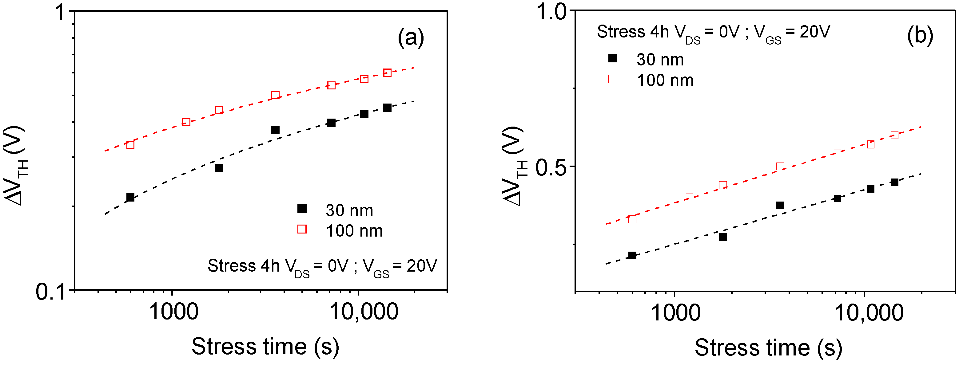
The same electrical stress as previously used was applied to TFTs with 30 nm and 100 nm thick channel layers. Figure 13 shows the variation in the threshold voltage of these TFTs under the application of +20 V gate voltage for 4 h, plotted in a logarithmic graph (log(ΔVTH) − log(t)) (a) or a semi-logarithmic graph (ΔVTH − log(t)) (b). The variation is lower when the channel layer’s thickness is lower. The electrical stability improves when the thickness of the channel layer decreases.
The plots are much more linear when using a semi-logarithmic scale than a logarithmic one. The semi-logarithmic plots lead us to conclude that the threshold voltage shift is due to the charge injection inside the gate insulator during the positive gate stress for both thicknesses.
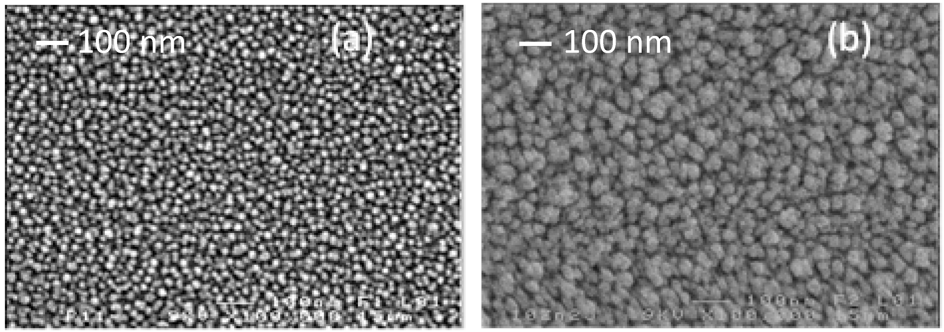
Therefore, the better stability of the thinner channel layer TFT confirms the general trend of the stability of TFTs if the structure is stable and does not change sensibly when the thickness changes. Figure 14 shows the surface of 30 nm and 100 nm thick as-deposited crystalline silicon as seen from SEM observations. It shows a similar uniform structure with adjacent grains. Only the grain size increases from 20 nm to 60 nm for the 30 nm and 100 nm thick films, respectively. In this case, and without a state creation during the stress, the thicker film allows for more electron injection inside the insulator leading to a greater trapped negative charge inside the insulator and more shift in the gate voltage.

4. Conclusions

The behavior of the electrical parameters of TFTs with the thickness of the channel layer is explained using only electrostatic arguments without referring to the used semiconducting material. Indeed, a general trend is found in the literature irrespective of the material if only the thickness changes without any other change (no structural variation, no uniformity change). It is possible to find other variations in the literature, but this is generally due to a change in uniformity for a very thin layer (a few nanometers) or some sensible change in the physical structure. The general trend consists of an increase in the threshold voltage, a decrease in the subthreshold slope, and better stability under gate bias stress when the thickness of the channel layer decreases.
The shift in the threshold voltage under positive gate bias is attributed mainly to charge trapping inside the gate insulator.

Author Contributions

Conceptualization, M.L.S., E.J., A.S.M. and T.M.-B.; experiment, M.L.S., E.J.; data analysis, M.L.S., E.J., A.S.M. and T.M.-B.; writing—original draft preparation, M.L.S. and A.S.M.; supervision, T.M.-B.; and writing—review and editing, A.S.M. and T.M.-B. All authors have read and agreed to the published version of the manuscript.

Funding

This research received no external funding.

Acknowledgments

The authors want to acknowledge the three laboratories and the three universities for their administrative and technical support.

Conflicts of Interest

The authors declare no conflict of interest.

References

  1. Sasaki, N.; Togei, R. Effect of silicon film thickness on threshold voltage of SOS-MOSFETs. Solid State Electron. 1979, 22, 417–421. [Google Scholar] [CrossRef]
  2. Colinge, J. Subthreshold slope of thin-film SOI MOSFETs. IEEE-EDL 1986, 7, 244–246. [Google Scholar] [CrossRef]
  3. Hsiaoi, T.C.; Wang, A.W.; Saraswat, K.; Woo, J.C.S. An alternative gate electrode material of fully depleted SOI CMOS for low power applications. In Proceedings of the 1997 IEEE International SOI Conference, Fish Camp, CA, USA, 6–9 October 1997; pp. 20–21. [Google Scholar]
  4. Balestra, F.; Benachir, M.; Brini, J.; Ghibaudau, G. Analystical Models of Subthreshold Swing and Threshold voltage for thin- and Ultra-Thin-Film SOI MOSFETs. IEEE Trans. Electron. Devices 1990, 37, 2303–2311. [Google Scholar] [CrossRef]
  5. Hayashi, H.; Noguchi, T.; Oshima, T. Polysilicon Super-Thin-Fim Transistor (SFT). Jpn. J. Apply. Phys. 1984, 23, L819–L820. [Google Scholar] [CrossRef]
  6. Noguchi, T.; Hayashi, H.; Ohshima, T. Low Temperature Polysilicon Super-Thin-Film Transistor (LSTS). Jpn. J. Apply. Phys. 1986, 25, L121–L123. [Google Scholar] [CrossRef]
  7. Martin, S.; Chiang, C.-S.; Nahm, J.-Y.; Li, T.; Kanicki, J.; Ugai, Y. Influence of the Amorphous Silicon Thickness on Top-gate Thin-Film Transistor Electrical Performances. Jpn. J. Appl. Phys. 2001, 40, 530–537. [Google Scholar] [CrossRef] [Green Version]
  8. Barquinha, P.; Pimentel, A.; Marques, A.; Pereira, L.; Martins, R.; Fortunato, E. Influence of the semiconductor thickness on the electrical properties of transparent TFTs based on indium zinc oxide. J. Non-Crystalline Sol. 2006, 352, 1749–1752. [Google Scholar] [CrossRef]
  9. Wang, Y.; Sun, X.; Goh, G.; Demir, H.; Yu, H. Influence of the Channel Layer Thickness on the Electrical Performance of Inkjet-Printed In-Ga-Zn Oxide Thin Film Transistors. IEEE Trans. Electron. Devices 2011, 58, 480–485. [Google Scholar] [CrossRef] [Green Version]
  10. Wang, D.; Furuta, M.; Tomai, S.; Yano, K. Understanding the role of Temperature and Drain Current Stress in InSnZnO TFTs with Various Active Layer Thickness. Nanomaterials 2020, 10, 617. [Google Scholar] [CrossRef] [Green Version]
  11. Kim, D.-H.; Cha, H.-S.; Jeong, H.-S.; Hwang, S.-H.; Kwon, H.-I. Effects of Active Layer Thickness on the Electrical Characteristics and Stability of High-Mobility Amorphous Indium-Gallium-Tin Oxide Thin-Film Transistors. Electronics 2021, 10, 1295. [Google Scholar] [CrossRef]
  12. Kandoussi, K.; Simon, C.; Coulon, N.; Mohammed-Brahim, T.; Moreac, A. Undoped and arsenic-doped low temperature (~165 °C) microcrystalline silicon for electronic devices. J. Non-Cryst. Sol. 2006, 352, 968–971. [Google Scholar] [CrossRef]
  13. Belarbi, K.; Kandoussi, K.; Coulon, N.; Simon, C.; Cherfi, R.; Fedala, A.; Mohammed-Brahim, T. Stability of microcrystalline silicon TFTs. ECS Trans. 2009, 23, 121–130. [Google Scholar]
  14. Samb, M.; Dong, H.; Jacques, E.; Sissoko, G.; Seidou-Maiga, A.; Mohammed-Brahim, T. Thinning the active layer of TFTs. ECS Trans. 2014, 64, 9–16. [Google Scholar] [CrossRef]
  15. Kandoussi, K.; Simon, C.; Coulon, N.; Belarbi, K.; Mohammed-Brahim, T. Nanocrystalline silicon TFT process using silane diluted in argon-hydrogen mixtures. J. Non-Cryst. Solids 2008, 354, 2513–2518. [Google Scholar] [CrossRef]
  16. Samb, M.L. Modelisation de Transistors en Couches Minces (TFT) Fabriques en Technologies Silicium Microcristallin Tres Basse Temperature. PhD Thesis, University of Rennes 1, Paris, France, 2014. [Google Scholar]
  17. SILVACO International. ATHENA User’s Manual, Device Simulation Software; SILVACO International: Santa Clara, CA, USA, 2008. [Google Scholar]
  18. SILVACO International. ATLAS User’s Manual, Device Simulation Software; SILVACO International: Santa Clara, CA, USA, 2008. [Google Scholar]
  19. Cho, E.; Kang, J.; Yun, I. Effects of channel thickness variation on bias stress instability of InGaZnO thin-film transistors. Microelectron. Reliab. 2011, 51, 1792–1795. [Google Scholar] [CrossRef]
  20. Jackson, W.; Marshall, J.; Moyer, M. Role of hydrogen in the formation of metastable defects in hydrogenated amorphous silicon. Phys. Rev. B 1989, 39, 1164–1179. [Google Scholar] [CrossRef] [PubMed]
  21. Chamberlin, R.; Mozurkewich, G.; Orbach, R. Time Decay of the Remanent Magnetization in Spin-Glasses. Phys. Rev. Lett. 1984, 52, 867–870. [Google Scholar] [CrossRef]
  22. Grassberger, P.; Procaccia, I. The longtime properties of diffusion in a medium with static traps. J. Chem. Phys. 1982, 77, 6281–6284. [Google Scholar] [CrossRef]
  23. Meaudre, R.; Meaudre, M.; Jensen, P.; Guiraud, G. Thermal-equilibrium processes and electronic transport in undoped hydrogenated amorphous silicon. Phil. Mag. Lett. 1988, 57, 315–320. [Google Scholar] [CrossRef]
  24. Jeppson, K.; Svenson, C. Negative Bias Stress of MOS Devices at High Electric Fields and Degradation of MNOS Devices. J. Appl. Phys. 1977, 48, 2004–2014. [Google Scholar] [CrossRef] [Green Version]
  25. Powell, M.; Van Berkel, C.; Hughes, J. Time and temperature dependence of instability mechanisms in amorphous silicon thin film transistors. Appl. Phys. Lett. 1989, 54, 1323–1325. [Google Scholar] [CrossRef]
  26. Young, N.; Ayres, J. Negative Gate Bias Instability in Polycrystalline Silicon TFTs. IEEE Trans. Electron. Devices 1995, 42, 1623–1627. [Google Scholar] [CrossRef]
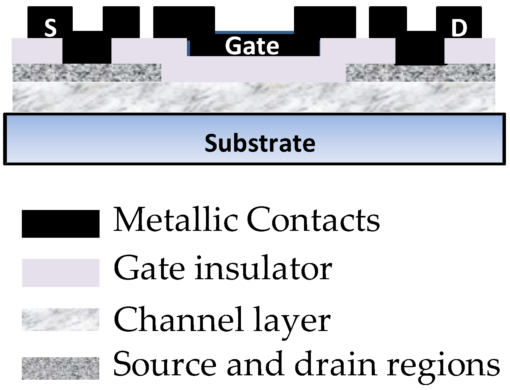
Figure 1. N-type Top-Gate Top-Contacts as-deposited crystalline silicon TFTs.
Electronics 12 02694 g001
Figure 2. Transfer characteristics of W = 100 µm/L = 20 µm sized transistors with a 30 nm, 100 nm, 200 nm thick channel layer. The thickness of the silicon nitride gate insulator is 300 nm.
Electronics 12 02694 g002
Figure 3. Crystalline fraction of as-deposited micro-poly crystalline silicon films with different thicknesses deposited in our conditions. The fraction is deduced from Raman measurements. Adapted from [15].
Electronics 12 02694 g003
Figure 4. Topography of the surface of 100 nm thick (area 15 µm × 15 µm) and 1 µm thick (area 30 µm × 30 µm) microcrystalline silicon layers analyzed by Atomic Force Microscopy.
Electronics 12 02694 g004
Figure 5. Threshold voltage and subthreshold swing as a function of the thickness of the single crystalline silicon TFTs, as deduced from the Silvaco model.
Electronics 12 02694 g005
Figure 6. Dependence of the subthreshold swing on the channel layer thickness when the channel material has no defect (single crystalline silicon) or contains defects (silicon with disordered structure). The values are calculated using Silvaco software modeling and the subthreshold slope is defined as previously. The curves were obtained in the linear regime with +1 V drain voltage.
Electronics 12 02694 g006
Figure 7. Silvaco software modeling of the profile of the potential under the insulator–channel layer interface for the 3 values of the channel layer thickness used in the experimental results. Either the channel material has no defect (single crystalline silicon) (left curve) or contains defects (silicon with disordered structure) (right curve). The curves were obtained with neither an applied gate voltage nor a drain voltage.
Electronics 12 02694 g007
Figure 8. Simulated profile of the free electron concentration under the insulator–channel layer interface for 3 values of the channel layer’s thickness when using a single crystalline silicon (without defects) channel or a disordered structure silicon (with defects) channel. The curves were obtained with neither an applied gate voltage nor a drain voltage.
Electronics 12 02694 g008
Figure 9. Transfer characteristics of a 100 nm thick channel layer and a W = 100 µm/L = 20 µm sized TFT submitted to a gate voltage of +20 V whenever the drain and source are short-circuited. The curves are plotted every 10 min and the stress is applied at 20 °C for 6 h.
Electronics 12 02694 g009
Figure 10. The fit (red line) of the experimental variation of the threshold voltage under the application of +20 V gate voltage stress whenever the drain and source are short-circuited at 20 °C. The fit uses the stretched exponential equation.
Electronics 12 02694 g010
Figure 11. Density of the energy states in a disordered semiconductor. Defect states are present in the forbidden gap between the minimum of the extended states’ conduction band EC and the maximum of the extended states’ valence band EV.
Electronics 12 02694 g011
Figure 12. Variation in the threshold voltage under the application of +20 V gate voltage for 6 h at 20 °C, 35 °C and 50 °C plotted using logarithmic (a) or semi-logarithmic (b) scales.
Electronics 12 02694 g012
Figure 13. Variation of the threshold voltage of TFTs with 30 nm and 100 nm thick channel layers under the application of +20 V gate voltage for 4 h plotted in logarithmic (a) or semi-logarithmic (b) scales.
Electronics 12 02694 g013
Figure 14. SEM observation of the surface of 30 nm (a) and 100 nm (b) thick as-deposited crystalline silicon layers. The grain size is 20 nm and 60 nm for the 30 nm thick and the 100 nm thick layers, respectively.
Electronics 12 02694 g014
Table 1. Electrical parameters of 3 TFTs with a 30 nm, 100 nm and 200 nm thick channel layer. t is the thickness of the channel layer. µ is the electron mobility. SS is the subthreshold swing and ION/IOFF is the ratio of the highest on-current to the lowest off-current. The grain size g of the silicon channel layer as deduced from Scanning Electron Microscopy observations is given in the last column.
T
(nm)
µ
(cm2/V.s)
SS
(V/dec)
VTH
(V)
ION/IOFFg
(nm)
300.410.386>10720
1000.520.93.510660
2000.631.92−1.210570
Disclaimer/Publisher’s Note: The statements, opinions and data contained in all publications are solely those of the individual author(s) and contributor(s) and not of MDPI and/or the editor(s). MDPI and/or the editor(s) disclaim responsibility for any injury to people or property resulting from any ideas, methods, instructions or products referred to in the content.