Article

Hardware Design and Implementation of a Lightweight Saber Algorithm Based on DRC Method

Faculty of Electrical Engineering and Computer Science, Ningbo University, Ningbo 315211, China
*
Authors to whom correspondence should be addressed.
Electronics 2023, 12(11), 2525; https://doi.org/10.3390/electronics12112525
Submission received: 11 May 2023 / Revised: 25 May 2023 / Accepted: 29 May 2023 / Published: 3 June 2023
(This article belongs to the Special Issue Computer-Aided Design for Hardware Security and Trust)

Abstract

:
With the development of quantum computers, the security of classical cryptosystems is seriously threatened, and the Saber algorithm has become one of the potential candidates for post-quantum cryptosystems (PQCs). To address the problems of long delay and the high power consumption of Saber algorithm hardware implementation, a lightweight Saber algorithm hardware design scheme based on the joint optimization of data readout and clock (DRC) was proposed. Firstly, an analysis was carried out on the hardware architecture, timing overhead and power consumption distribution of the Saber algorithm, and the key circuits that limit the performance of the algorithm were identified; secondly, a dual-port SRAM parallel reading method was adopted to improve the data reading efficiency and reduce the timing overhead of double data reading in the multiplier module. Then, a clock gating technology was used to reduce the dynamic flipping probability of internal registers and reduce the hardware power consumption of the Saber algorithm; finally, data reading and clock gating were jointly optimized to design a high-speed and low-power Saber algorithm hardware IP core. Lightweight IP cores were integrated into RISC-V SoC systems via APB bus in a TSMC 65 nm process to complete the digital back-end design. The experimental results show an IP core area of 0.99 mm2 and power consumption of 8.49 mW, which is 33% lower than that reported in the related literature. Under 72 MHz & 1 V operating conditions, the number of clock cycles for the Saber algorithm’s key generation, encryption and decryption are 3315, 9204 and 1420, respectively.

1. Introduction

Quantum computing breaks through existing computing architectures and uses the principle of state superposition to make quantum computers a research hotspot. For example, in 2019, Google developed a superconducting quantum chip [1] circuit that samples a billion times faster than conventional computers; in 2020, the University of Science and Technology of China built a photonic quantum computing prototype, “Jiuzhang” [2], which is trillions of times faster than existing supercomputers; in 2022, the Institute for Molecular Science in Japan announced that its quantum research has produced the world’s highest speed in the quantum computer “2-bit quantum gate”. With the development of quantum computers, the number of quantum bits has increased dramatically, and the security of cryptosystems based on mathematical puzzles such as classical large integer decomposition and discrete logarithms has been greatly challenged. In classical computer architecture, the underlying mathematical problems on which traditional cryptography relies are extremely difficult to solve in an efficient time. However, in the face of quantum computers, mathematical difficulties based on public-key cryptosystems will no longer be secure [3], so the information security systems and various applications built by relying on cryptosystems will face serious security problems, and there is an urgent need for research on cryptosystems and chip implementation technologies to resist quantum attacks. Given the extensive applications of public key cryptography, such as network security, data storage, and autonomous driving, the development of ciphers resistant to quantum attacks poses significant technical challenges. Specifically, it involves the task of effectively unifying security with the efficiency and flexibility required for hardware implementation.
The National Institute of Standards and Technology (NIST) announced a call for Post-Quantum Cryptosystem (PQC) standards in February 2016, with plans to formally complete the standardization of PQC by 2024. The first round of the competition screened 69 candidate algorithms, and 26 candidate algorithms were retained in the second round. After three rounds of screening, seven PQC solutions, including Saber, Kyber, and Falcon, entered the final evaluation. Among them, the Saber [4] algorithm is a lattice-based key encapsulation mechanism (KEM) that works against chosen ciphertext attack (CCA), and its security depends on the difficulty of the module learning with rounding (MLWR) problem. Lattice-based cryptographic problems, such as the shortest vector problem (SVP) and closest vector problem (CVP), are not susceptible to quantum computing. Among various quantum-resistant cryptographic schemes, lattice-based approaches are particularly promising due to their robust security against quantum attacks, higher computational efficiency, and flexible applications. This is why the lattice-based grid code scheme occupied five out of the seven candidates selected by NIST for the third round of standardization. The Saber algorithm differs from other lattice-based schemes in that it is modulo 2 to the power of 2, which eliminates the need for additional overhead in modulo operations and the rejection of sampling operations. Consequently, the research focus in cryptography revolves around the theoretical study and efficient hardware implementation of Saber’s algorithm. The Saber algorithm mainly involves three steps: key generation, encryption, and decryption, and the security core lies in the random number expansion and large matrix product module, which has the characteristics of fast computing speed and functional diversity, compared with other algorithms [5,6,7]. To reduce the operation overhead of the Saber algorithm, Knuth et al. [8], a team of algorithm proposers, constructed a fast polynomial computation method for the multiplier module in conjunction with the Toom–Cook general algorithm, which effectively improved the operational efficiency of the large matrix product module of the Saber algorithm. To further optimize the Saber algorithm, Sujoy et al. [9] used vector processing instructions to process the algorithm operations in parallel, resulting in a nearly 1.5-fold increase in throughput, while increasing the latency of individual operations by a factor of about 3. In terms of hardware–software co-design, Mera et al. [10] and Dang et al. [11] used a hardware–software co-design strategy to allocate hardware–software resources for cryptographic algorithms through software algorithms, which can achieve high-speed and flexible cryptographic algorithms. Although hardware–software co-design has obvious advantages in terms of flexibility in algorithm implementation, there are still shortcomings in terms of latency and throughput, so hardware implementation of algorithms has become a research trend. Roy et al. [12] implemented a high-speed dot matrix Saber algorithm on FPGA, with a running time of 61.4 μs at a clock frequency of 250 MHz. To meet the requirements of the Saber algorithm in resource-constrained situations, and to reduce the running time and power consumption of the algorithm hardware [13,14,15,16,17], there is an urgent need to study lightweight cryptographic algorithms. Based on this, this design constructs the algorithm model based on the official documentation [18] of the algorithm, and thus completes the full hardware implementation of Saber’s algorithm.
This paper proposes a lightweight Saber algorithm hardware internet protocol (IP) core based on joint optimization of data readout and clock (DRC). First, to solve the timing overhead problem caused by the dual data reading of the Saber algorithm multiplier module, the memory module was optimized using a dual-port SRAM technology to improve the operation speed of the multiplier module. Then, the probability of dynamic flip-flop power consumption was reduced by adding a clock gating unit circuit and a clock reset hosting signal. IP cores were integrated into the RISC-V SoC using an advanced peripheral bus (APB) approach. Finally, a TSMC 65 nm digital back-end based design was completed.

2. Introduction to the Saber Algorithm

2.1. Symbolic Representation

This section introduces some preparatory knowledge, including basic definitions and symbols. We use bold lowercase letters to represent vectors, such as a, and use bold uppercase letters to represent matrices, such as A. For a polynomial f, we write fi for the ith coefficient of xi. p and q are integer powers of 2, p = 2 ε p and q = 2 ε q . We use Z q to denote the ring of integers modulo integer q with representants in [0, q), and for an integer z, z mod q denotes the mode approximate reduction of z in the interval [0, q). Rq = Z q [x]/(xn + 1) denotes the ring of integer polynomials modulo (xn + 1), where n is a power of 2 and each coefficient of the ring is in [0, q). For any ring R, RL × K denotes the ring on the matrix L × K. β μ denotes the central binomial distribution, with μ being an even number and a distribution ranging from [−μ/2, μ/2]. The l-value represents the matrix dimension in the Saber algorithm, and the value of l in Saber is 3. The l-value in LightSaber is 2 and in FireSaber is 4, where l = 2 means lightweight encryption, l = 3 means standard security level encryption, and l = 4 means high-security level encryption.

2.2. Saber Algorithm Process

The Saber algorithm is a lattice-based encryption and decryption mechanism that resists selective ciphertext attacks. Lattice-based cryptographic algorithms can be constructed from two different problems, namely, the lattice-based shortest vector problem and the lattice-based nearest vector problem. The learning with error (LWE) problem is based on the nearest vector problem on a general lattice, and the learning with rounding (LWR) problem can be reduced to the shortest vector problem on a lattice. In contrast to the LWE problem, the noise of the LWR is generated deterministically, avoiding the randomness attached to the noise. Mod-LWE replaces a single ring element with modulo element on the same ring, and is an improved version of LWE. Similarly, Mod-LWR is an improved version of Mod-LWE with smaller ciphertext bandwidth compared to Mod-LWE. The security of Saber algorithm depends on Mod-LWR and has the advantage of being lightweight. The Saber algorithm implementation includes public key encryption (PKE) and the key encapsulation mechanism (KEM). PKE is an IND-CPA secure encryption scheme, and KEM is an IND-CCA secure key encapsulation mechanism, with both implementations consisting of key generation, encryption and decryption algorithms.
The Saber algorithm PKE key generation pseudo-code is shown in Algorithm 1. PKE key generation starts by reading seedA, which is a key seed signal, through a register, and using the random number expansion module SHAKE128 function to process the seed signal for randomness. The random number matrix A is generated by the gen function based on the seed signal seedA. The matrix A is an l × l matrix and the key s is an l × 1 matrix, where the individual matrix elements are polynomials of order 256. In the hardware implementation of the Saber algorithm, the l value is 3, and the individual elements of s take the value interval [−4: 4]. In Algorithm 1, the random number matrix is transposed and multiplied by the key matrix. The matrix transposition operation, vector-to-string operation, and public key splicing operation can be carried out in hardware by changing the read address bits, which improves the efficiency of the algorithm compared to the software implementation of these operations. The secret key generation phase of PKE generates public key pk and private key sk, matrix b and seedA are stitched to obtain public key pk, and matrix S is assigned to sk after vector-to-string operation.
Algorithm 1 Saber.PKE.KeyGen()
s e e d A μ ( { 0 ,   1 } 256 ) A = g e n ( s e e d A ) R q l × l r = μ ( { 0 ,   1 } 256 ) s = β μ ( R q l × 1 ;   r ) b = ( ( A T s + h ) mod q ) ( ε q ε p ) R p l × 1 return   ( p k : = ( s e e d A ,   b ) ,   s k : = ( s ) )
PKE encryption is shown in Algorithm 2. Firstly, a random number matrix A is generated by the gen function, and a new key matrix s’ is generated in the encryption algorithm. The product of matrix A and s’ is rounded and shifted to produce b as the [0: 512] bits of the ciphertext, and the [513: 1024] bits of the ciphertext cm are generated by the shift algorithm module and the encryption module.
Algorithm 2 Saber.PKE.Enc (pk = (seedA, b), mR2; r)
if   r   i s   n o t   s p e c i f i e d   then   r = μ ( { 0 ,   1 } 256 ) s = β μ ( R q l × 1 ;   r ) b = ( ( A s + h ) mod q ) ( ε q ε p ) R p l × 1 v = b T ( s mod p ) R p c m = ( v + h 1 2 ε p 1 m mod p ) ( ε q ε T ) R T return   c : = ( c m ,   b ) = ( s e e d A ,   b ) ,   s k : = ( s ) )
PKE decryption is shown in Algorithm 3, the received encrypted data are first modulo approximately subtracted and then transposed, and the value after the operation enters the product module. The decryption data are given after the shift operation to realize the operation of extracting the plaintext from the ciphertext.
Algorithm 3 Saber.PKE.Dec (sk = s, c = (cm, b’))
v = b T ( s mod p ) R p m = ( ( v 2 ε q ε T c m + h 2 ) mod p ) ( ε p 1 ) R 2 return   m
The above is the IND-CPA encryption process, and the CPA security component can be constructed using the Fujisaki–Okamoto transformation for the IND-CCA security KEM. IND-CCA contains three steps: key generation, encryption and decryption. The algorithm achieves encryption and decryption by invoking the key generation, encryption and decryption operations in IND-CPA. The difference between the KEM algorithm and the PKE encryption algorithm is that the former returns a randomly generated string when the public key decapsulation fails, making the algorithm more secure. The KEM key generation calls the PKE key generation process to obtain the public and private keys through numerical stitching and assignment, which is a non-clock consuming operation in the hardware implementation, and is implemented directly through address bit calls.
KEM key generation, KEM encapsulation and decapsulation are shown in Algorithms 4–6. The plaintext m and the public key pk are randomized in KEM encryption by the SHA3-256 function in the random number expansion module to obtain the processed m and HASH-pk, and kr’ is obtained by the data bit splicing operation. The kr’ is processed by the SHA3-256 function to obtain the upper half of the session key returned by the KEM encryption operation, and the lower half of the session key returned by the KEM operation is the plaintext generated in the PKE.
Algorithm 4 Saber.KEM.KeyGen()
( s e e d A ,   b ,   s ) = S a b e r . P K E . K e y G e n ( ) p k = ( s e e d A ,   b ) p k h = ( p k ) z = μ ( { 0 ,   1 } 256 ) return   ( p k : = ( s e e d A ,   b ) ,   s k : = ( s ,   z ,   p k h ,   p k ) )
Algorithm 5 Saber.KEM.Encps(pk = (seedA, b))
m μ ( { 0 ,   1 } 256 ) ( K ^ ,   r ) = G ( ( p k ) ,   m ) c = S a b e r . P K E . E n c ( p k ,   m ;   r ) K = ( K ^ ,   c ) return   ( c ,   K )
The ciphertext is obtained by calling the PKE decryption algorithm in KEM decapsulation, and a verification module is added to the algorithm to verify the correctness of the plaintext. If the public key decapsulation fails, a randomly generated string will be returned to improve the resistance to attacks.
Algorithm 6 Saber.KEM.Decaps(sk = (z, pkh, pk, s)
m = S a b e r . P K E . D e c ( s ,   c ) ( K ^ ,   r ) = G ( p k h ,   m ) c = S a b e r . P K E . E n c ( p k ,   m ;   r ) if   c = c   then   return   K = ( K ^ ,   c ) ; else   return   K = H ( z ,   c )

3. Hardware Implementation of Saber Algorithm

The previous section introduced the Saber algorithm key generation and encryption/decryption algorithm. The algorithm computation module consists of a hash function, a polynomial product function, and a shift function. Since p and q are powers of 2 in the Saber algorithm, the hardware implementation does not require modulo reduction operations, and the Keccak core gas pedal is designed to be low-power and fast in hardware. The algorithm hardware IP core implementation is described as follows, and the design of each module of Saber algorithm is specified as follows.

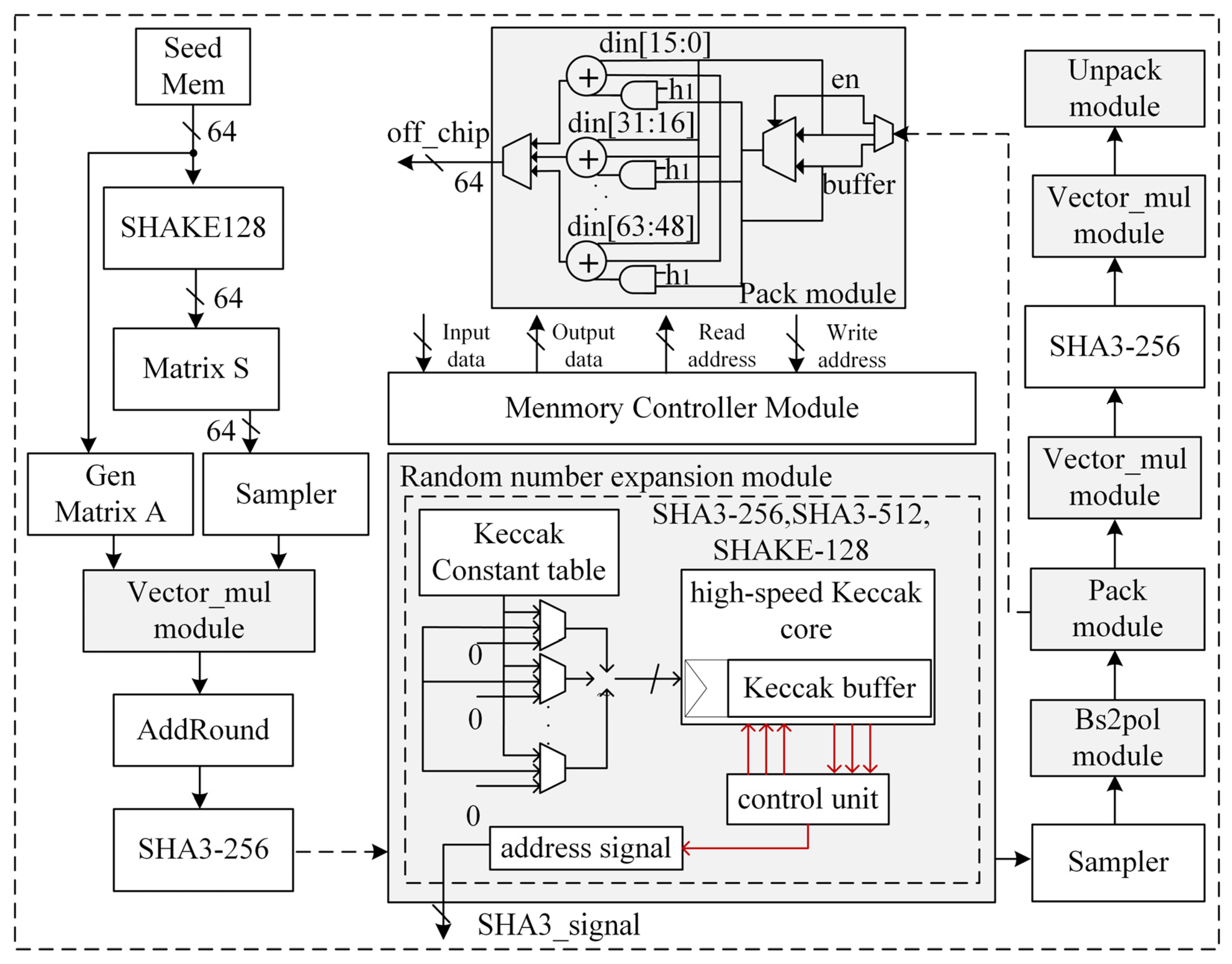
3.1. Saber Algorithm Hardware Architecture

The overall hardware IP architecture of the Saber algorithm is shown in Figure 1. The hardware IP architecture of the Saber algorithm encompasses several key components, including a random number expansion module, a binomial sampling module, a multiplier module, a shift module, a string conversion module, an encryption module, a decryption module, a signal control module, a communication control module, and a memory module. The signal control unit module ensures a uniform distribution of input and output data flow for each module. It connects the enable signal, data signal, and address signal of each module, while intermediate data generated during the algorithm execution are stored in the memory module. When integrating the IP through the APB bus, the external port includes various signals, such as the reset signal, enable signal, write data signal, read data signal, write enable signal, address signal, clock signal, chip select signal, and off-chip output signal. The off-chip output signal is specifically designed to output the encrypted ciphertext. According to the Saber algorithm flow, the hardware data flow state machine is designed.
The hardware IP structure of the low-power Saber algorithm is shown in Figure 2. First, a memory module composed of eight SRAMs is used, and the external circuits include a multiplier module, a sampling module, a SHA-3 random number expansion module, an encryption module, a decryption module, a multiplier module, and a string conversion module. The read/write signals and input/output data of each module are connected to the register control module. According to the algorithm principle, Seed is used as the input signal to the IP core, then the data are processed by each module, and the intermediate data are stored in the register module. The algorithm is created based on the data flow of the algorithm and the input/output port control of the memory module.

3.2. Single-Cycle Double Data Reading and Storage Module Design

The data storage module is the intermediate value reading/writing unit, which is the hardware core module of the IP core. The algorithm involves performing multiple matrix multiplications with large random number matrices, such as matrix AT*s in Algorithm 1 and A*s in Algorithm 2. Consequently, the storage module of the algorithm’s IP core incurs significant overhead in terms of read clock cycles during the data reading process. The conventional memory module is a single-port memory module which has the problem of excessive timing overhead, incurred by reading a set of data per clock. This paper proposes a dual-port memory module design; by using a dual-port SRAM memory module, two sets of coefficients can be read out in one clock cycle, which results in a two-fold increase in overall performance at the cost of a small area. In practice, the storage and recall of data is controlled by the write address and the read address. The data are processed by different modules, such as multiplier module, and random number expansion to complete the data processing in three modes of key generation, encryption and decryption. Data reading and writing is performed in memory through 64-bit transfer operations. This data selection method facilitates integration with the processor (32-bit or 64-bit).
The memory structure is shown in Figure 3. The whole memory module is divided into four SRAMA and four SRAMB, and the size of an individual SRAM is 1024 × 16 bits. Each SRAMA single clock output has 16 bits, the four SRAMA output values are stitched together, and the overall output is a single clock output of 64 bits. SRAMB operates on the same principle.
SRAMA and SRAMB enable control signals, read/write control signals and read/write address signals to be input to the memory module through the signal control module. The off-chip output of the cipher text is accomplished by locating the fixed storage cells of the memory module.
The plaintext of the encrypted data is generated by the random number expansion module and entered into a predetermined unit of the memory module. The encrypted and decrypted data will be input to the fixed storage unit of the memory module. For the IP core, the top-level encryption and decryption can be used as the encryption IP or decryption IP separately, and both share the random number expansion module, binomial sampling module, polynomial multiplication module, and string steering module, which can effectively reduce the hardware overhead of the Saber algorithm IP core.

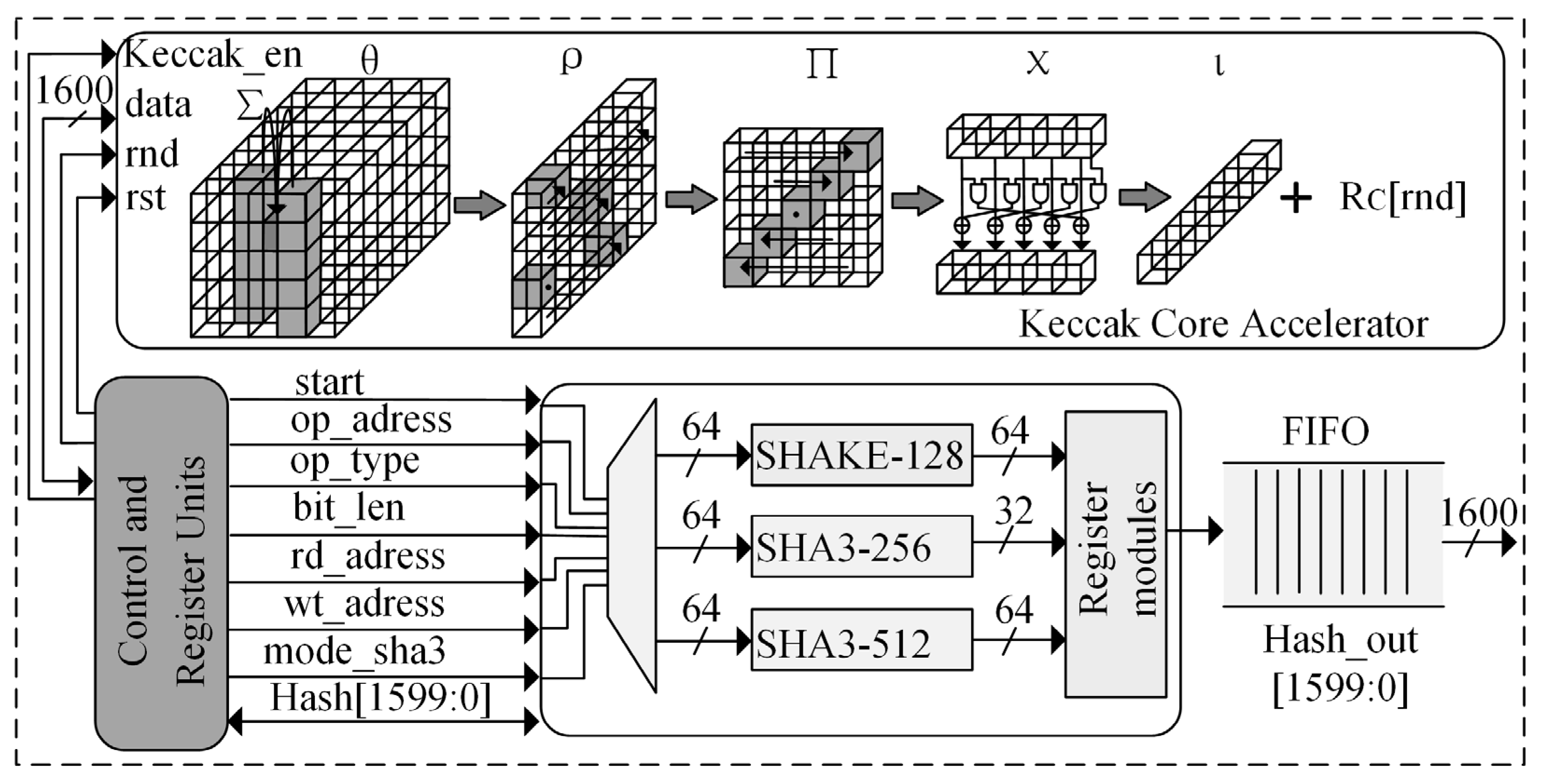
3.3. High-Speed Random Number Expansion Module Circuit Design

The implementation of the Saber algorithm involves SHAKE-128, SHA3-256 and SHA3-512 functions, and a random number function selector is used in the random number module for different computational function selections. The random number generation hardware circuit structure is shown in Figure 4. The random number module is controlled by the data control module, and the control port occupies 6 data bits of control signal, which is the total control signal of Saber IP. These 6 bits of data are used to control the random number generation function type and data length, respectively, where the control signal is customized by the initial module. In the random number module, the Keccak core acceleration module is instantiated with 1600 data bits.
The core acceleration module has five steps: θ, ρ, , χ, ι. The input and output arrays of the module are states A and B, with a width of 1600 bits, respectively. The states can be represented by a three-dimensional array containing 25 words, each with a length of 64 bits. Words can constitute a cube with x, y and z coordinates. Each bit of the cube can be addressed by [x, y, z]. The states are specified as follows: the state of a word is called a “Lane”, the two-dimensional part with a concrete coordinate having a fixed z-value state is called a “Slice”, and all “Lanes” with the same x-coordinates are called “Sheets” [19].
Step θ: This step first calculates the state C[x] = A[X, 0] ⊕ [x, 1] ⊕ A[x, 2] ⊕ A[x, 3] ⊕ A[x, 4], where x takes values in the range [0, 4], and the output of the θ step can be expressed as B[x, y] = A[x, y] ⊕ (C[x − 1] ⊕ rot(C(x + 1) + 1). Step ρ rotates Lane by an offset r[x, y], which depends on the values of x, y. Thus, the equation for this step can be expressed as B[x, y] = rot(A[x, y], r[x, y]), Step can be expressed as B[y, 2x + 3y] = A[x, y], and this step is equivalent to swapping the states of the Lane. Steps χ and ι: Step χ can be expressed using the formula B[x, y] = A[x, y] ⊕ ( A ¯ [x + 1, y) & (A[x + 2, y). In step ι, the constant Rc is anisotropic with Lane, and this step can be expressed as B [0, 0] = A[0, 0] ⊕ Rc[i], with the constant value depending on the current number of rounds i.
The multiplier module mainly implements the multiplication of matrix A and key matrix S. In the Saber algorithm, the l-value is 3, so matrix A is a 3 × 3 matrix, and matrix S is a 3 × 1 matrix. The mode selection side was added to the product module to support polynomial coefficients of both 13-bit and 10-bit bit widths, as defined by the Saber algorithm. The dual-port SRAM can read multipliers simultaneously in a single cycle, which can further increase the multiplication speed and complete the IP core design for the high-speed Saber algorithm.

3.4. Lightweight Encryption and Decryption Hardware Module Design

In algorithm encryption and decryption operations, a mode control signal was added to the IP top layer to control the IP core for encryption and decryption by assigning values to the mode console and the enable side. The IP performs key generation operation when the mode console is 01, encryption operation when the value is 10, and decryption operation when it is 11. The processing data was fed to different units to complete the multiplexing of multiplication modules, random numbers, and other modules in the encryption and decryption process, thus reducing the hardware area of the IP core. The intermediate data will be stored in SRAM after being processed by different modules, and the bit splicing operation will be completed by changing the initial bit of the read address.
The output timing of the encrypted IP core is shown in Figure 5. During the encryption of the IP core, the off-chip port provides the ciphertext data, and the mode value is at this point 01. When the encryption module enable signal jumps from high to low, it indicates that the encryption is complete. When the encryption module enable signal jumps from high to low, it indicates that the encryption is complete. The write enable signal jumps from low to high and begins to read the ciphertext data. The output cipher text of the encryption module is 16 × 64 bits, with 64 bits of data being output in each clock, and after 16 clocks, the off_chip_done signal jumps to a high level, at which point the cipher text is all output.

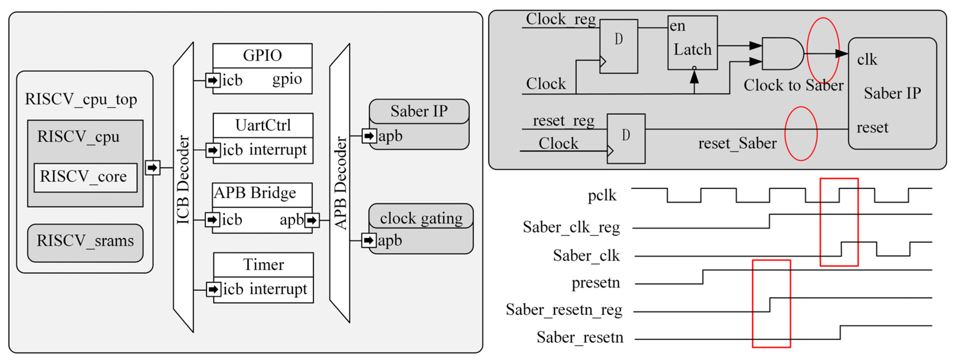
3.5. Processor-Level Low-Power Implementation of the Saber Algorithm IP Core

The hardware IP core of the Saber algorithm is integrated into the System on Chip (SoC) system via the APB bus, and the clock, reset and enable signals of the IP core are given by the SoC, as shown in Figure 6. The design uses the Hummingbird e203 processor. The reduction of dynamic flip power consumption is particularly important in IP core integration. This integration includes a clock gating circuit that connects to the bus, which reduces the dynamic flip power consumption of the entire IP core. The clock gating circuit uses clock and reset hosting signals to control the signal flipping of the Saber algorithm IP core. In the gated clock output timing, the system clock and reset signals are fed into the Saber algorithm IP core when the clock and reset signal register signals jump high, inserting a simultaneous global clock gating in the back-end design.
The memory module register addresses assignments when the Saber algorithm IP core is mounted via APB bus, as shown in Table 1. The table gives the offset addresses for different ports, their read/write permissions and register definitions. When the processor reads the off_chip_done signal indicating that encrypted data is output, the processor hands over other signals, such as the clk signal and Start signal, to the IP core. The segment base address of the APB bus is 0x10007000. With bit 0 of the SABER_CLK_ADDR register being 1, there would be a clock for the IP core, and with bit 0 being 0, there would be no clock. A system reset is used when bit 0 of the SABER_RESETN_ADDR register is 1, and a clock is used when bit 0 is 0. Bit 0 of the START_ADDR register is used to receive the Start signal, and bits [1: 0] of the MODE_ADDR register are used to receive the mode signal.

4. Experimental Results and Analysis

This section presents the experimental results of the Saber algorithm. The co-processor is described in Verilog language, and the algorithm consists of a data control module and a calculation module. The experimental process uses the EDA simulation tool VCS, a logic synthesis tool design compiler, a physical layout tool IC compiler, the Cadence layout design tool IC5141 and the Mentor graphical interface Calibre to complete the back-end design of this IP based on the TSMC 65 nm process under the standard process tcbn65gplustc, where the IP core storage module consumes eight 1024 × 16 SRAMs.

4.1. Algorithm Performance Results

The number of execution cycles and time for the Saber algorithm KEM back-end design in different modes of key generation, encryption, and decryption are shown in Table 2. The key generation phase consumes 3304 clock cycles, the encryption phase consumes 4704 clock cycles, and the decryption consumes 1420 clock cycles. For high-performance data reading, the memory module consists of 8 × 1024 × 16 SRAMs.
The proposed IP core was implemented under the operating conditions of 72 MHz clock frequency and 1 V supply voltage. The IP core area is 0.65 mm2, and the chip layout is shown in Figure 7. The design of the dual-port SRAM and the clock gating circuitry does not provide a distinct advantage in terms of the area of the IP core compared to existing implementations. However, this design primarily focuses on optimizing the timing and power consumption. The back-end design of this IP core is based on the TSMC 65 nm process, and the equivalent logic gate count of the IP core after conversion is 45 K. The power consumption shares of the multiplier module, register module, random number expansion module, encryption and decryption module, string conversion module, and main control module of the Saber algorithm hardware IP are shown in Figure 7.
The power consumption shows that by adding the gated clock unit circuit, the power consumption of the IP core at different frequencies can be reduced by 50%, as shown in Figure 8. Using different process corners to complete the back-end design, the power consumption of the IP core at different frequencies with supply voltages of 1.1 V, 1 V, 0.9 V and 0.8 V is shown in Figure 8. The power consumption of the IP core decreases with a reduction in supply voltage. According to the power consumption report, the power consumption of the IP core does not change much when the supply voltage varies from 1 V to 0.9 V; therefore, this design is chosen to complete the backend design under the standard process tcbn65gplustc, with a voltage of 1 V.
When the plaintext data are shown on the left side of Table 3, the ciphertext data generated by the encryption module are shown on the right side of Table 3. The bit width of the plaintext data is 256, and the bit width of the ciphertext data is 1024. The ciphertext output is achieved by reading the fixed memory cell of SRAM.

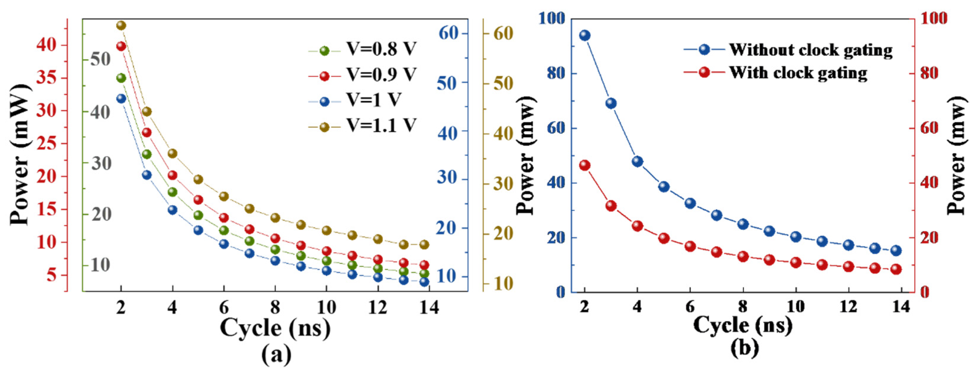
4.2. Power Area Analysis of IP Cores

The back-end design is completed using different process corners at 72 MHz operating frequency with the various processes of tcbn65gplustc0d8, tcbn65gpluswc, and tcbn65gplustc at supply voltages of 0.8 V, 0.9 V, and 1 V, respectively. Within this design, we have analyzed the area and power consumption values for multiple modules, such as Mul (multiplier), SHA (random number expansion), Dpram (memory), Addh (shift), Bol2pol (string conversion), Bin (binomial sampling), Pack (encryption), and Unpack (decryption). These analyses were conducted at different supply voltages of 1 V, 0.9 V, and 0.8 V for various processes. The trends of area and power consumption values of each module of the IP core are shown in Figure 9. Due to the hardware adaptability of the random number expansion module, its power consumption and area consumption are at a low level. The power consumption of multiplier module is the primary concern for the IP core. Our next objective is to decrease the power consumption of the multiplier module.

4.3. Comparison with Related Literature

A comparison of the hardware implementation of this design with other post-quantum cryptographic algorithms is shown in Table 4. The comparison involves different post-quantum cryptographic algorithms, including different implementation methods such as hardware–software co-implementation and hardware implementation, as well as involving different implementation platforms and different operating frequencies. For the different schemes using different platforms and different implementations, the relevant data show that the proposed scheme has significant advantages in terms of speed and power consumption. The all-hardware implementation [20,21] was faster than the hardware–software collaborative design, and the random number acceleration core module, Keccak, ran slower when implemented on a software platform, with the timing overhead being higher when implemented using software code on Keccak. A comparison of the time and power consumption of the back-end design completed using the TSMC 65 nm process with other post-quantum cryptographic algorithm hardware implementations is shown in Table 4. Study [10], study [11], and the current design all involve software/hardware implementations of the Saber algorithm. With the same flow of the algorithm, the comparison focuses on the power consumption and area of the algorithm implementation. While the study referenced in [11] achieves lower running time, it does not hold an advantage in hardware consumption compared to the study referenced in [10]. In contrast, this design leverages ASIC implementation, which offers advantages in terms of the overall running time for secret key generation, encryption, and decryption. Furthermore, it increases the size of the IP chip to some extent, thereby enhancing the algorithm’s speed. In terms of experimental environment, the comparison with study [21] is more similar, and the running time of the secret key generation, encryption, and decryption modes is significantly reduced during the double data reading session due to the presence of multiple sizeable random number matrix products in the algorithm process. Including the clock gating unit circuit in the bus integration and the insertion of the global clock gating in the back-end design reduces the power consumption of the IP core significantly, and this design still dominates at 72 MHz operating frequency. The global clock insertion has reduced the dominance of equivalent logic gates, but the algorithm’s runtime and power consumption are significantly optimized. In terms of runtime, the overall architecture of this design is nearly 100 times faster compared to the other two design solutions. The results show that this design has a faster speed and relatively lower power consumption.

5. Conclusions

This study completes the design of a hardware IP core for Saber algorithm. Based on the analysis of the Saber algorithm structure, the data reading efficiency was improved by using a dual-port SRAM parallel reading method for the timing overhead problem caused by the data reading of the multiplier module. To address the problem of the clock dynamic power consumption of the IP core, the clock gating technique was used to reduce the probability of internal register dynamic flipping, thus reducing the hardware power consumption of the IP core. Finally, the digital back-end design was completed by integrating lightweight IP cores into the RISC-V SoC system via the APB bus within the TSMC 65 nm process. The Saber algorithm is a strong contender as a post-quantum cryptographic algorithm due to its omission of the mode about subtraction operation, which means it has a better prospect of achieving lightweight post-quantum cryptographic encryption. In our future work, we plan to conduct a more comprehensive analysis of the application’s resistance to known attacks and potential vulnerabilities. This analysis aims to enhance the algorithm’s overall resilience against attacks by addressing any identified vulnerabilities from an application perspective.

Author Contributions

Conceptualization, W.Z. and H.Z.; methodology, Y.Z., H.Z. and W.Z.; software, W.Z. and Y.W.; investigation, J.L.; writing—original draft preparation, W.Z., L.N. and Z.L.; writing—review and editing, H.Z., J.L. and Y.W.; supervision, Y.Z. All authors have read and agreed to the published version of the manuscript.

Funding

This research was funded by the National Natural Science Foundation of China (grant no. 62174121, 61871244, 62134002), the Science and Technology Innovation 2025 Major Project of Ningbo City (grant no. 2022Z203), the Fundamental Research Funds for the Provincial Universities of Zhejiang (grant no. SJLY2020015), the S&T Plan of Ningbo Science and Technology Department (grant no. 202002N3134), the K. C. Wong Magna Fund at Ningbo University for Science, the General Research Project for Education Department of Zhejiang Province (grant no. Y202249923), and the Fresh Talent Program for the Science and Technology Department of Zhejiang Province (grant no. 2022R405B082).

Data Availability Statement

Not applicable.

Conflicts of Interest

The authors declare no conflict of interest.

References

  1. Arute, F.; Arya, K.; Babbush, R.; Bacon, D.; Bardin, J.C.; Barends, R.; Biswas, R.; Boixo, S.; Brandao, F.G.; Buell, D.A. Quantum supremacy using a programmable superconducting processor. Nature 2019, 574, 505–510. [Google Scholar] [CrossRef] [PubMed] [Green Version]
  2. Zhong, H.; Wang, H.; Deng, Y.; Chen, M.; Peng, L.; Luo, Y.; Qin, J.; Wu, D.; Ding, X.; Hu, Y. Quantum computational advantage using photons. Science 2020, 370, 1460–1463. [Google Scholar] [CrossRef] [PubMed]
  3. Shor, P.W. Algorithms for quantum computation: Discrete logarithms and factoring. In Proceedings of the 35th Annual Symposium on Foundations of Computer Science, Santa Fe, New Mexico, 20–24 November 1994; pp. 124–134. [Google Scholar]
  4. Lee, D.H.; Seo, E.Y.; Kim, Y.S.; No, J.S. Rethinking on ciphertext equality check of decapsulation of nist pqc standardization 3rd round finalist candidate saber. In Proceedings of the 2022 13th International Conference on Information and Communication Technology Convergence (ICTC), Xi’an, China, 19–21 October 2022; pp. 1483–1486. [Google Scholar]
  5. Pöppelmann, T.; Güneysu, T. Towards practical lattice-based public-key encryption on reconfigurable hardware. In Proceedings of the Selected Areas in Cryptography—SAC 2013: 20th International Conference, Burnaby, BC, Canada, 14–16 August 2014; pp. 68–85. [Google Scholar]
  6. Roy, S.S.; Vercauteren, F.; Mentens, N.; Chen, D.D.; Verbauwhede, I. Compact ring-lwe cryptoprocessor. In Proceedings of the Cryptographic Hardware and Embedded Systems–CHES 2014: 16th International Workshop, Busan, South Korea, 23–26 September 2014; pp. 371–391. [Google Scholar]
  7. De Clercq, R.; Roy, S.S.; Vercauteren, F.; Verbauwhede, I. Efficient software implementation of ring-lwe encryption. In Proceedings of the Automation & Test in Europe Conference & Exhibition (DATE), Grenoble, France, 9–13 March 2015; pp. 339–344. [Google Scholar]
  8. Knuth, D.E. The Art of Computer Programming; Pearson Education: Boston, MA, USA, 1997; Volume 3. [Google Scholar]
  9. Roy, S.S. Saberx4: High-throughput software implementation of saber key encapsulation mechanism. In Proceedings of the 2019 IEEE 37th International Conference on Computer Design (ICCD), Abu Dhabi, United Arab Emirates, 17–20 November 2019; pp. 321–324. [Google Scholar]
  10. Mera, J.; Turan, F.; Karmakar, A.; Roy, S.S.; Verbauwhede, I.M. Compact domain-specific co-processor for accelerating module lattice-based kem. In Proceedings of the 2020 57th ACM/IEEE Design Automation Conference (DAC), San Francisco, CA, USA, 20–24 July 2020; pp. 1–6. [Google Scholar]
  11. Dang, V.B.; Farahmand, F.; Andrzejczak, M.; Gaj, K. Implementing and benchmarking three lattice-based post-quantum cryptography algorithms using software/hardware codesign. In Proceedings of the 2019 International Conference on Field-Programmable Technology (ICFPT), Tianjin, China, 9–13 December 2019; pp. 206–214. [Google Scholar]
  12. Roy, S.S.; Basso, A. High-speed instruction-set coprocessor for lattice-based key encapsulation mechanism: Saber in hardware. IACR Trans. Cryptogr. Hardw. Embed. Syst. 2020, 443–466. Available online: https://tches.iacr.org/index.php/TCHES/article/view/8690 (accessed on 26 August 2020). [CrossRef]
  13. Karmakar, A.; Mera, J.M.B.; Roy, S.S.; Verbauwhede, I.J.C.e.A. Saber on arm: Cca-secure module lattice-based key encapsulation on arm. Cryptogr. Hardw. Embed. Syst. 2018, 243–266. Available online: https://eprint.iacr.org/2018/682 (accessed on 14 August 2018). [CrossRef]
  14. Kannwischer, M.J.; Rijneveld, J.; Schwabe, P. Faster multiplication in z2m [x] on cortex-m4 to speed up nist pqc candidates. In Proceedings of the Applied Cryptography and Network Security: 17th International Conference, Bogota, Colombia, 5–7 June 2019; pp. 281–301. [Google Scholar]
  15. Liu, W.; Fan, S.; Khalid, A.; Rafferty, C.; O’Neill, M. Optimized schoolbook polynomial multiplication for compact lattice-based cryptography on fpga. Trans. Very Large Scale Integr. (VLSI) Syst. 2019, 27, 2459–2463. [Google Scholar] [CrossRef] [Green Version]
  16. Paksoy, I.K.; Cenk, M. Tmvp-based multiplication for polynomial quotient rings and application to saber on arm cortex-m4. Cryptol. ePrint Arch. 2020. Available online: https://eprint.iacr.org/2020/1302 (accessed on 19 October 2020).
  17. Zhu, Y.; Zhu, M.; Yang, B.; Zhu, W.; Deng, C.; Chen, C.; Wei, S.; Liu, L. Lwrpro: An energy-efficient configurable crypto-processor for module-lwr. Trans. Circuits Syst. I Regul. Pap. 2021, 68, 1146–1159. [Google Scholar] [CrossRef]
  18. Alagic, G.; Apon, D.; Cooper, D.; Dang, Q.; Dang, T.; Kelsey, J.; Lichtinger, J.; Miller, C.; Moody, D.; Peralta, R. Status Report on the Third Round of the Nist Post-Quantum Cryptography Standardization Process; US Department of Commerce: Washington, DC, USA, 2022.
  19. Fritzmann, T.; Sigl, G.; Sepúlveda, J. Risq-v: Tightly coupled risc-v accelerators for post-quantum cryptography. IACR Trans. Cryptogr. Hardw. Embed. Syst. 2020, 2020, 239–280. [Google Scholar] [CrossRef]
  20. Howe, J.; Oder, T.; Krausz, M.; Güneysu, T. Standard lattice-based key encapsulation on embedded devices. Cryptol. ePrint Arch. 2018, 2018, 372–393. [Google Scholar] [CrossRef]
  21. Oder, T.; Güneysu, T. Implementing the newhope-simple key exchange on low-cost fpgas. In Proceedings of the Progress in Cryptology–LATINCRYPT 2017: 5th International Conference on Cryptology and Information Security in Latin America, Havana, Cuba, 20–22 September 2017; pp. 128–142. [Google Scholar]
  22. Banerjee, U.; Ukyab, T.S.; Chandrakasan, A.P. Sapphire: A configurable crypto-processor for post-quantum lattice-based protocols. IACR Trans. Cryptogr. Hardw. Embed. Syst. 2019, 2019, 17–61. [Google Scholar] [CrossRef]
  23. Kuo, P.; Chen, Y.; Hsu, Y.; Cheng, C.; Li, W.; Yang, B. High performance post-quantum key exchange on fpgas. Cryptol. ePrint Arch. 2017, 37, 1211–1229. [Google Scholar]
  24. Basu, K.; Soni, D.; Nabeel, M.; Karri, R. Nist post-quantum cryptography-a hardware evaluation study. Cryptol. ePrint Arch. 2019. Available online: https://eprint.iacr.org/2019/047 (accessed on 25 January 2019).
Figure 1. Overall hardware IP architecture.
Electronics 12 02525 g001
Figure 2. Saber hardware IP diagram.
Electronics 12 02525 g002
Figure 3. Memory module.
Electronics 12 02525 g003
Figure 4. Hardware circuit structure for random number generation.
Electronics 12 02525 g004
Figure 5. Output timing diagram of the encrypted IP.
Electronics 12 02525 g005
Figure 6. Saber algorithm IP core SoC architecture.
Electronics 12 02525 g006
Figure 7. Hardware IP core back-end implementation diagram: (a) chip architecture diagram, (b) process information diagram, and (c) power consumption ratio of each module.
Electronics 12 02525 g007
Figure 8. Power consumption profiles: (a) power consumption trends of IP cores at different process angles, (b) power consumption profiles with and without clock gating.
Electronics 12 02525 g008
Figure 9. Power consumption area curves: (a) power consumption curves for each module of the IP core, (b) area curves for each module of the IP core.
Electronics 12 02525 g009
Table 1. Memory module register address allocation table.
Register DefinitionOffset AddressRead and Write Permissions
SABER_CLK_ADDR00Only write
SABER_RESETN_ADDR04Only write
START_ADDR08Only write
MODE_ADDR0COnly write
OFF_CHIP_DONE_ADDR10Only read
Table 2. Number of cycles and time of execution of Saber back-end design.
InstructionKeygenEncapsulationDecapsulation
Cycle (ns)330447021240
Times (us)44.09122.4119.89
Table 3. The plaintext data and the corresponding ciphertext data.
Plaintext [0,255] Ciphertext [0,511] Ciphertext [512,1024]
[0]8016_8f9b_2748_fb2f[0]a49c_7f6f_c0e7_6e42[8]2228_ef65_aeb3_2aac
[1]929d_ef22_2b56_9fda[1]2700_7850_7870_3409[9]f603_fd1b_12d6_104e
[2]4e91_9dab_35c4_0884[2]1f7a_caa5_c53e_1659[10]8ff8_4044_277e_d3f7
[3]baf4_f48b_4929_b385[3]9066_2771_c1e3_5f47[11]a632_b681_316d_3b42
[4]4f1a_1573_b02f_fb4c[12]dea4_d1b2_9047_f26d
[5]8ea5_ffbe_c8a5_1d19[13]00a5_9136_fedc_c541
[6]0004_0fe3_34e1_2f4b[14]d24f_2810_29a0_2c61
[7]c134_797a_646f_deb5[15]701c_41a4_727e_dc1a
Table 4. Comparison with existing post-quantum cryptographic schemes.
PaperSaber [10]Saber [11]Frodo [20]NewHope [21]Kyber [22]NewHope [23]Dilithium-II [24]This Work
TechnologyArtix-7
(HW/SW)
UltraScale+
(HW/SW)
Artix-7Artix-7ASIC
[TSMC 40 nm]
Artix-7ASIC
[TSMC 65 nm]
ASIC
[TSMC 65 nm]
Times in usKeygen3273-45,454988154851.9980.644.1
Encaps41476045,4541413245678.6122.4
Decaps38446547,619473164621.118.8
Frequency
(MHz)
1253221671677213115872
LUT7.4 K12.5 K7.7 K5.1 K-20 K--
FF7.3 K11.6 K3.5 K4.4 K-9.9 K--
DSP2825612-8--
BRAM24244-14--
Area (mm2)----0.28-4.70.99
VDD (V)----1.1-1.21
Area (K GATE)----106-1603451
Power (mW)----12.8-50.428.4
Disclaimer/Publisher’s Note: The statements, opinions and data contained in all publications are solely those of the individual author(s) and contributor(s) and not of MDPI and/or the editor(s). MDPI and/or the editor(s) disclaim responsibility for any injury to people or property resulting from any ideas, methods, instructions or products referred to in the content.

