1. Introduction
Injection locking is a well-known nonlinear phenomenon [
1]. It is a physical phenomenon of forced oscillation [
2]. When an external signal is applied to an oscillator, if the injected signal is close to its own oscillation frequency, the frequency of the oscillator will shift towards the injected signal. When the injected signal amplitude is large enough, the output frequency of the oscillator will remain the same as the input signal frequency, while there is a phase difference between the phase of the output signal of the oscillator and the phase of the injected signal [
3]. This phenomenon is widely used in communication systems, such as remote frequency calibration, antenna arrays, quadrature voltage-controlled oscillators (QVCOs), frequency dividers, frequency multipliers, clock recovery, etc. Meanwhile, injection locking can improve the phase noise of the voltage-controlled oscillator [
4,
5,
6].
Beam scanning is a technique that concentrates electromagnetic radiation and can focus transmitted or received signals in a specific direction or region to improve the performance and efficiency of the system. In communication, radar, survey and other fields, beam scanning has very important application value. The beam-scanning array has been developed gradually over the last decades, and many technologies, such as fast beam scanning, conformal with carrier, and beam-shape agility, have been widely used in communication systems and radar systems. With the development of electronic technology, the application of the beam scanning antenna array is becoming more and more common. Antenna arrays for beam scanning in phased arrays have proven to be a very promising technology for high-speed wireless networks. They combine signals from N different array elements. The beam directions can be adjusted in a desired way with the help of phase shifters. Therefore, phase shifters are an integral part of most antenna arrays. Conventional phase shifters are based either on distributed transmission line networks [
7] or hybrid couplers with tunable load reflections [
8]. However, they have high insertion losses and amplitude variations, and they require large areas. This brings great challenges in terms of miniaturization and low cost. Injection-locked techniques [
9] provide an efficient method to generate stable high-frequency signal sources and are used in phased arrays. We use injection locking technology to provide a reliable, small and scalable phase shifting system for the beam-scanning array antenna. We use the injection locking phase characteristic of the VCO to realize the phase change of the array.
Injection-locked oscillators can be used as continuous phase shifters for applications in beamforming networks [
10]. This can be achieved using injection-locked oscillator arrays (ILOAs) or coupled oscillator arrays (COAs) [
11]. By adjusting the free-running frequency of these oscillators, linear phase steps on the oscillator can be obtained [
12]. Such oscillator arrays can be used as local oscillators (LOs) [
13] or fed directly to antenna elements [
14] for beamforming. They can be used to achieve synchronous operation of multiple antenna elements and allow manipulation of the phase distribution without the need for additional phase-shifting circuitry. This technique has the additional advantages of generating an output signal with excellent phase noise despite the low-quality factor of the VCO [
15].
In a classical COA, all oscillators are interconnected through a coupling network. Phase progression in the oscillators is attained either by modifying the free-running frequency of the oscillators at both ends [
16] or by varying the phase difference between these two oscillators using a phase shifter [
11]. Since weak coupling within the antenna array restricts the locking bandwidth, strong coupling is employed to boost mutual synchronization [
17]. However, as the number of strongly coupled oscillators increases, the number of bad modes also increases, which can affect the stability of the oscillation frequency and must be considered in the circuit design [
18]. The maximum attainable phase difference between the two end oscillators in a COA is ±90°. Nevertheless, due to the coupling network, altering the output signal of one oscillator necessitates the control of both this oscillator and the frequencies of the oscillators on the two adjacent sides.
Recognizing the limitations of traditional injection-locked oscillator arrays, we aimed to find a solution that would realize the phase controlling of the array using only one external signal without any extra phase shifters. It will simultaneously decrease the coupling between array elements to the extent that the phase controlling of a single stage could be independently controlled by the VCO at that stage. We proposed a cascading injection-locked oscillator array. In our experiments, we found that eliminating the coupling between oscillators was challenging. Nevertheless, we were able to reduce the coupling, where its effect on the phase was only transmitted between neighboring oscillators. Based on this, we designed a cascaded injection-locked oscillator array with weak reverse coupling, which employed a one-dimensional array of four VCOs.
Section 2 analyzes the maximum locking bandwidth, locking condition, and phase noise of the locked oscillator under multi-signal injection. In
Section 3, the phase behavior in the cascaded injection-locked oscillator array with weak reverse coupling is examined. Based on these analyses, an injection-locked oscillator array consisting of VCOs is introduced, and in
Section 4, the measurement results of the proposed VCO array are presented. Finally, in
Section 5, conclusions are drawn.
2. Study on Injection Locking Oscillator with Multiple Signals
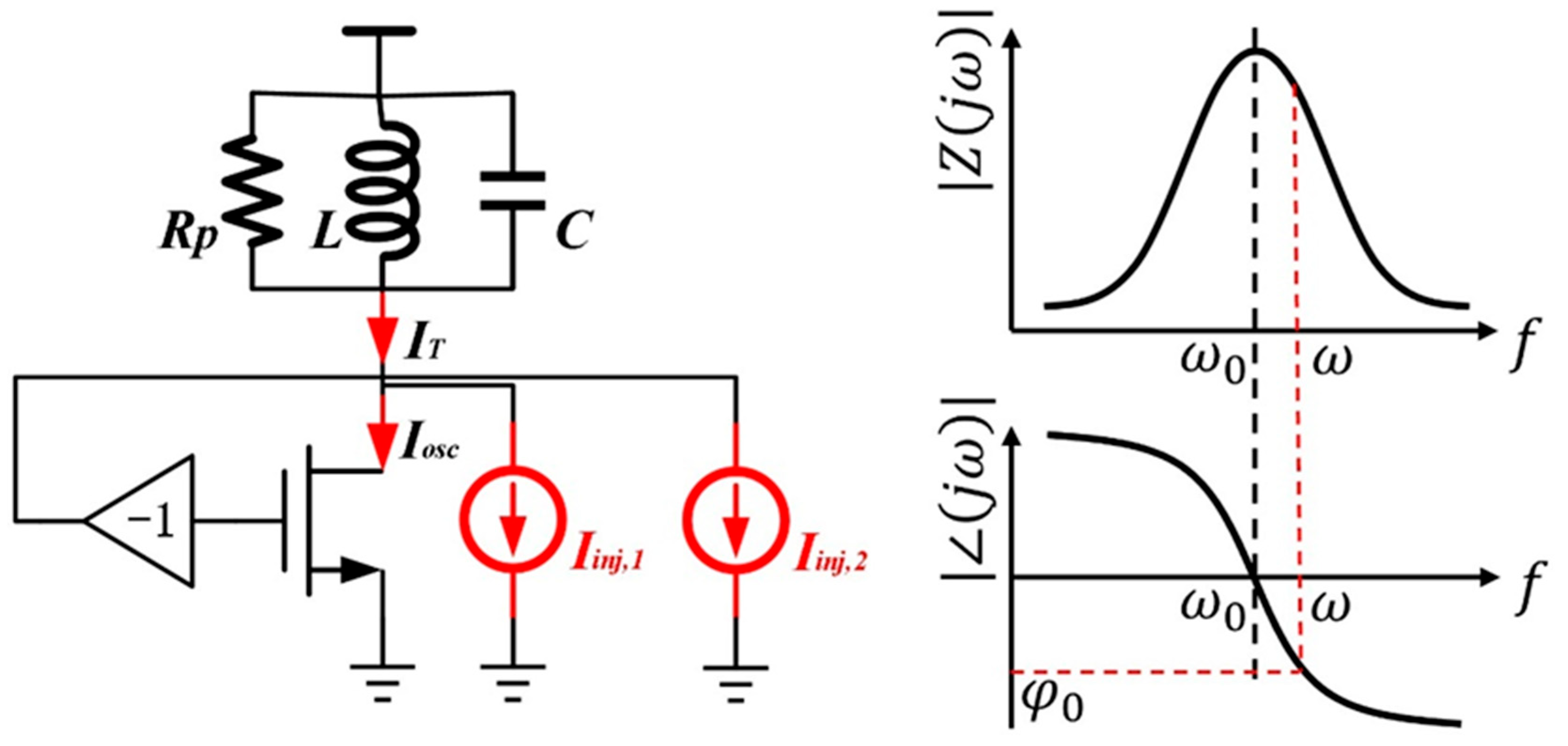
A conceptual injection-locked oscillator is shown in
Figure 1.
Rp is the equivalent parallel resistance of the inductor. The free-running oscillation output frequency is
. Under the injection of external signals, the frequency of the oscillator output signal changes to
. Considering
there will be
where
. The phase shift of the tank can be derived in a simplified way as
where
represents the quality factor of the tank.
The total current on the reactance in the tank is zero when the oscillator is operating at the free frequency. Meanwhile, the contribution of this tank to the phase shift in the feedback network is zero.
Figure 1 shows two independent signals (
and
) injected into the oscillator simultaneously. Then, the current in the tank is supplied by an externally injected current source [
19], At the same time, the output frequency of the oscillator will be shifted from
.
Since the total current on the reactance in the tank is zero, a phase shift in feedback will be introduced. The oscillator operating at any other frequency is prohibited by a phase shift introduced by the tuned circuit, where the total current on the reactor is no longer zero. Now, the output frequency of the oscillator at this time is
, although it can never complete a cycle of motion at this frequency [
20], making it is a transient concept. However, the feedback signal
must be in phase with
through the feedback network. This means the angle between
and
is such that
becomes aligned with
after experiencing the tank phase shift
at instantaneous frequency
.
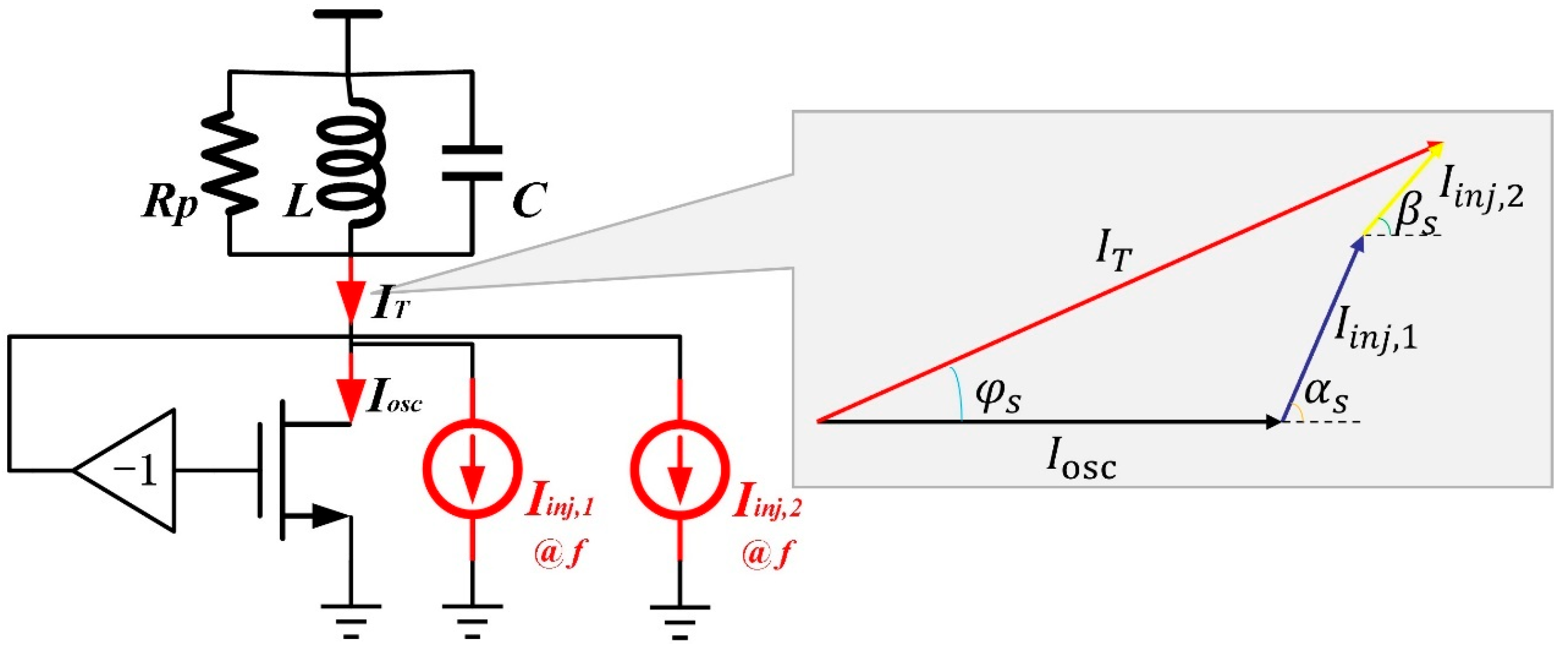
Figure 2 shows the vector diagram of the potentials shown in
Figure 1. In
Figure 2, the vector representing the external signal (
) is at rest with respect to the observer. Therefore, the vector at rest in the diagram has an angular frequency and a phase angle equal to that of the angular frequency and phase angle of external signal
. The other vectors rotate counterclockwise around
. The angular frequency of the other vectors is equal to the angular frequency relative to
plus the angular frequency of
itself. At this time, the output frequency of the oscillator is
, where
denotes the angular frequency of the oscillator with respect to the injected signal
, and
is the angular frequency of the injected signal
. There is the same pattern in the phase. The locking Equation (2) can be obtained from
Figure 2.
where
and
where
and
is a set of constants, which stand relative to time.
,
are the instantaneous phase angles of the first and second injected signals, which are a function of time
t.
is the instantaneous phase angle of output of the injected oscillator, which is also a function of time
t.
is the phase shift of the tank under injection. From (1), it follows that
By making these substitutions and rearranging (3), the locking equation is obtained:
Equation (4) describes the behavior of the output phase of the oscillator under two-signal injection. Similarly, we can obtain the performance of the oscillator output phase under multi-signal injection.
where
and
denote the amplitude and phase of the
injected signal. All angles in the equation are a function of time
t. We consider whether the output phase of the oscillator can reach steady state under two-tone injection. In this case, the left side of (5) is a constant. However, the right side of the equation is an expression containing the variable
t. According to the theory of harmonic balance, the condition for this equation to hold in this case is
The frequency of all injected signals is equal to the frequency of the oscillator output signal, which means that the oscillator will be locked when all injected signals are at the same frequency. In this case, the maximum locking range
will be determined by the injection ratio of each signal.
where
denotes the injection ratio for each signal injected separately into the oscillator. Referring to the expression for the maximum locking range, the required signal for locking is obtained when the injected-signal frequency is
. We define
.
then
When (8) is satisfied, the oscillator can only be locked at frequency under multi-signal injection. denotes the sum of the power of all injected signals, and N is the number of external signals.
When a signal is injected into an oscillator, the phase noise of its output signal depends on both the phase noise of the injected signal and the phase noise of the oscillator itself under free operation, as well as the offset of the injected signal frequency with respect to the free output frequency of the oscillator. When there are multiple independent signals injected into the oscillator simultaneously, it is worth studying the phase noise of the oscillator output signal.
The phase perturbation of the injected signals always affects the phase behavior of the output signal. If the output envelope does not change significantly, as in the case of small perturbations, the injection ratio does not change either. ILO always compensates for small phase or frequency perturbations. Since noise is a small signal, it is possible to model the noise behavior of an ILO using small-signal analysis.
First, consider the case where the oscillator is locked at two signals of the same frequency. According to (4), the equation is re-expressed as
where
Figure 3 shows a schematic diagram of the oscillator stabilizing the output phase when locked.
and
are the phase difference between the first and second signals with the output signal.
and
are the phase of the first and second signals.
and
are the frequency and phase of the oscillator output signals.
is the free-running oscillation output frequency. Now, there is a perturbation in the phase of these signals. Then, replace
,
,
and
of (6) with
,
,
and
, respectively, and the new equation is expressed as
Since
and
are tiny quantities, Equation (10) can be approximated as
where
Note that these perturbations model the phase noise of the injection source and the stand-alone oscillator. Since it was assumed that the disturbances are small, all higher order terms in (11) have been neglected. Transforming both sides of (11) to the Laplace domain, we obtain
Assume that all noise is an uncorrelated random process with zero time average. Then, the phase noise of an oscillator injected by two signals is denoted as
where
,
,
and
represent ILO, oscillator, the first source and the second source phase noise and
is the frequency offset at which the phase noise is calculated. From (13), the phase noise of the oscillator output depends on the phase noise of each source, as well as the phase noise of the oscillator when it oscillates freely, and also on the phase difference between the injected signal and the oscillator output signal and the injection ratio. The phase difference is another manifestation of the frequency shift. An ILO high-pass filter filters the oscillator noise, while a low-pass filter filters the injection sources’ noise.
When a signal is injected into an oscillator, the phase noise of the oscillator is influenced by the injection ratio of the two injected signals. The higher the sum of the two injection signal ratios, the better the phase noise performance.
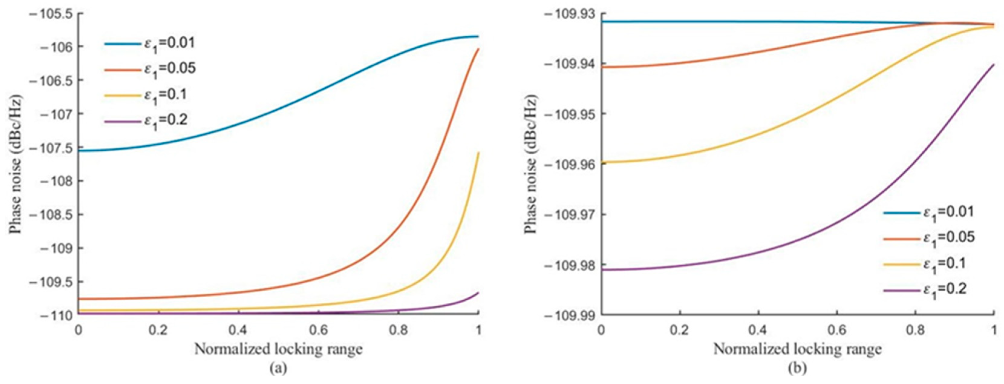
Figure 4 shows that the phase noise of the oscillator output signal gradually deteriorates as the phase difference increases (as the injection frequency gradually moves away from the free frequency of the oscillator). Phase noise is worse at frequencies far from the center frequency. With small signal injection (injection ratio less than 0.1), at the locking band edge, any disturbance may cause the ILO to be temporarily unlocked and disconnected from the input. At this point, the phase noise at the output of the oscillator is close to the phase noise of its free-oscillation mode.
As shown in
Figure 4, the increase of the injection ratio improves the phase noise of the oscillator signal, which is now closer to the phase noise of the injected signal. As shown in
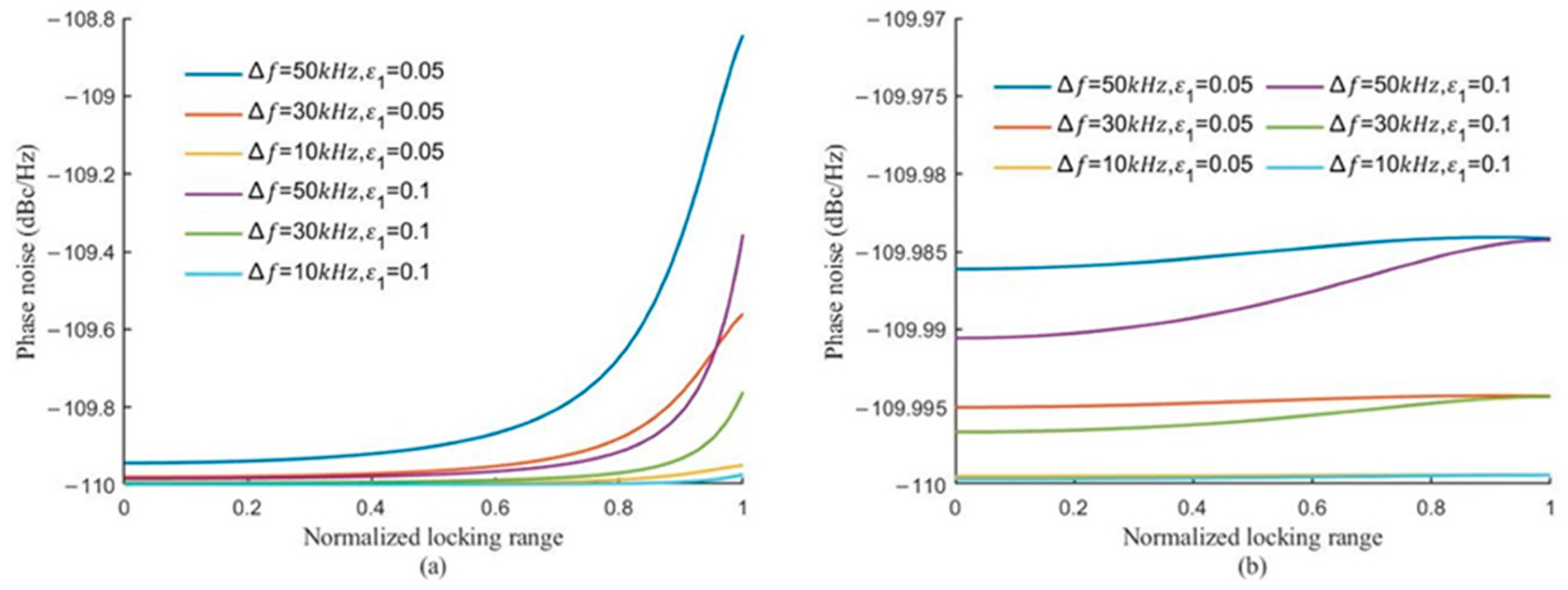
Figure 5, as the injected power of one of the two signals increases, the fluctuation of the phase noise of the oscillator output signal decreases with the change in phase difference within the locking bandwidth.
Now, we consider the performance of high frequency noise near the central frequency. According to (13), we obtain
where
When the phase noise of two injected signals is equal, the phase noise of the output signal of the oscillator is equal to the phase noise of injected signal. Meanwhile, the change in phase difference has little effect on the phase noise of the output signal, as shown in
Figure 6.
Now, we assume that the phase noise of the first one is better than the second one, where
Then, the phase noise of this oscillator in this bandwidth is limited between the phase noise of two injecting signals.
Figure 7 shows the relationship between the phase noise of the oscillator output signal and the phase difference
,
. The phase noise of the oscillator output signal gradually deteriorates with the increase of
. However, it improves with the increase of
, since
becomes smaller as
increases with
fixed. Unlike the performance of a single signal-locked oscillator, with two signal-locked oscillators, the phase noise of the output signal is still very good, despite the fact that one of the signals is on the edge of locking. Any perturbation causes the ILO to be temporarily outside the lock range, when all signals are on the edge of the locking band.
Similarly, one can express the phase noise of an oscillator injected by multiple signals.
where
Equation (15) can be mapped onto the equivalent block diagram shown in
Figure 8.
represents the phase difference between the
signal and the oscillator output signal at steady state.
represents the phase noise of the
injecting signal at steady state. The phase noise of the oscillator output will depend on the phase noise of each injected source, while the phase noise will vary with the phase difference between each injected signal and the oscillator output signal. Eventually, when all signal frequencies reach the edge of locking band, the oscillator will be out of locking.
3. Circuit Description and Analysis
3.1. A VCO Injected at the Voltage Tuning Port
In conventional designs, oscillators are injection-locked at the microwave output port using a circulator. However, this design expands the area of the dielectric substrate used. A good voltage-controlled oscillator chip has good reverse-isolation performance at the output port. This results in very little power being used to pull the VCO when it is injected with a larger power external signal.
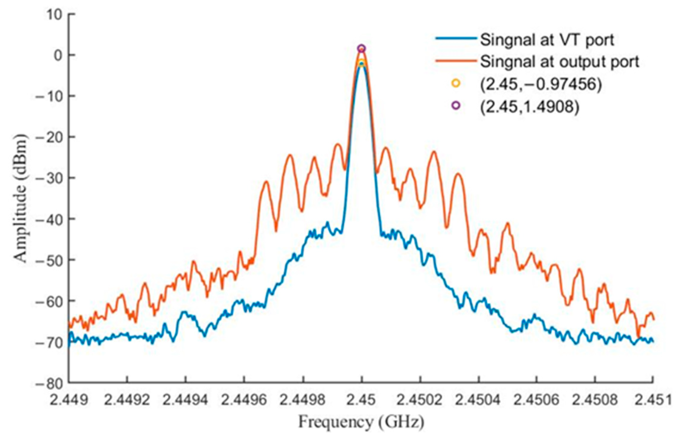
In this circuit design, the MVE2400 model VCO chip was used, operating in the frequency band of 2300 to 2500 MHz with an output power of 3 dBm at 2.45 GHz. The voltage tuning port (VT port) leaked microwave signal as well. Its power decreased only 2.5 dB relative to the power at the output port. The spectrum of the VCO at the output and voltage tuning ports are shown in
Figure 9.
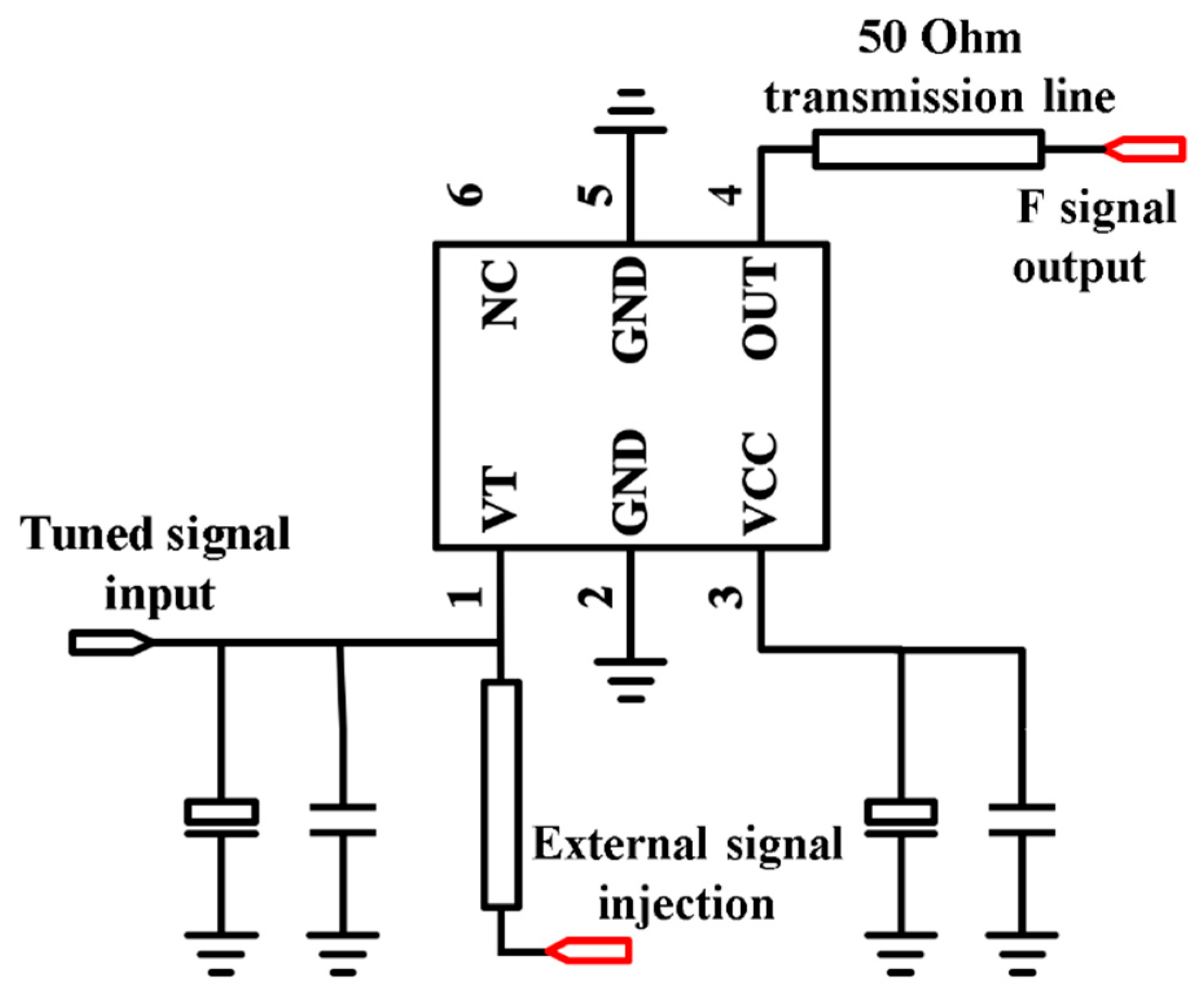
In this chip, the performance of microwave isolation at the voltage tuning port is poor. This means that microwave signals can be injected directly into the VCO at this port without using any circulators. Although the low-cost VCO chip has poor signal isolation performance, this makes it possible to implement an inexpensive, fabricated-on-chip phase-shifter for phased arrays.
Figure 10 illustrates the circuit schematic of the injection-locked VCO.
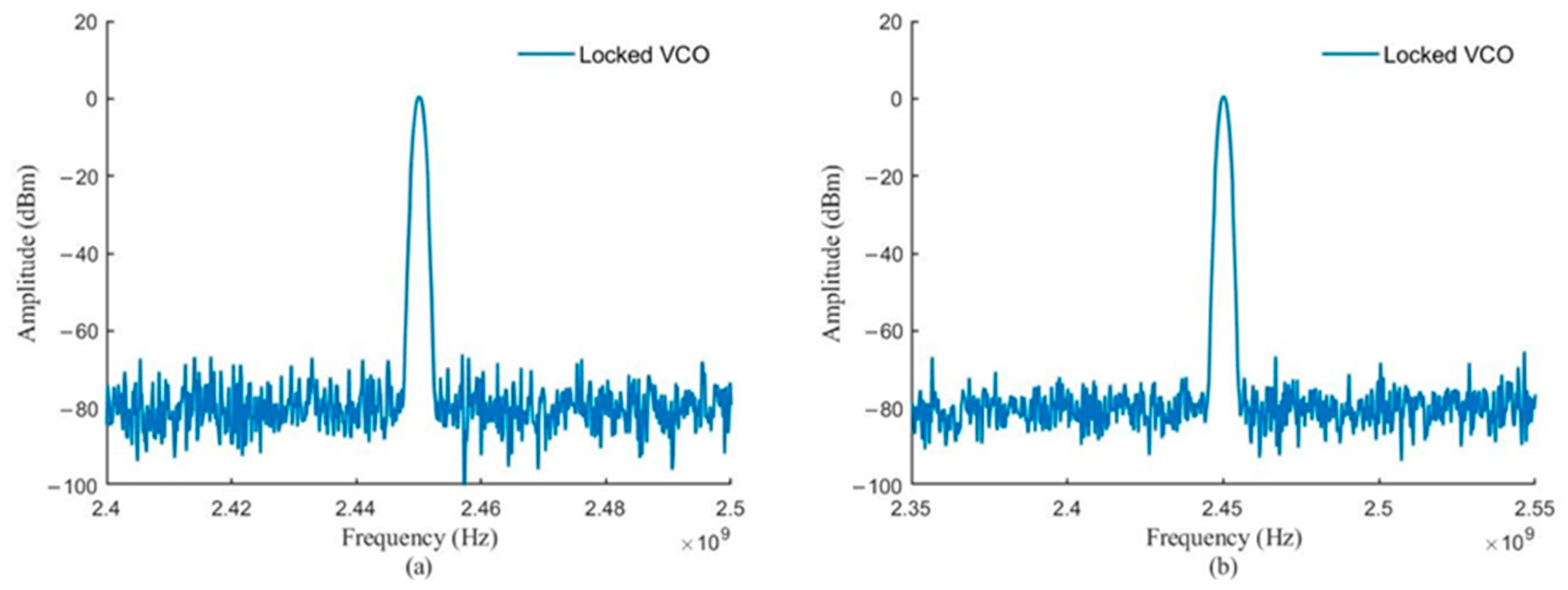
Figure 11 demonstrates that the VCO is locked at an external signal.
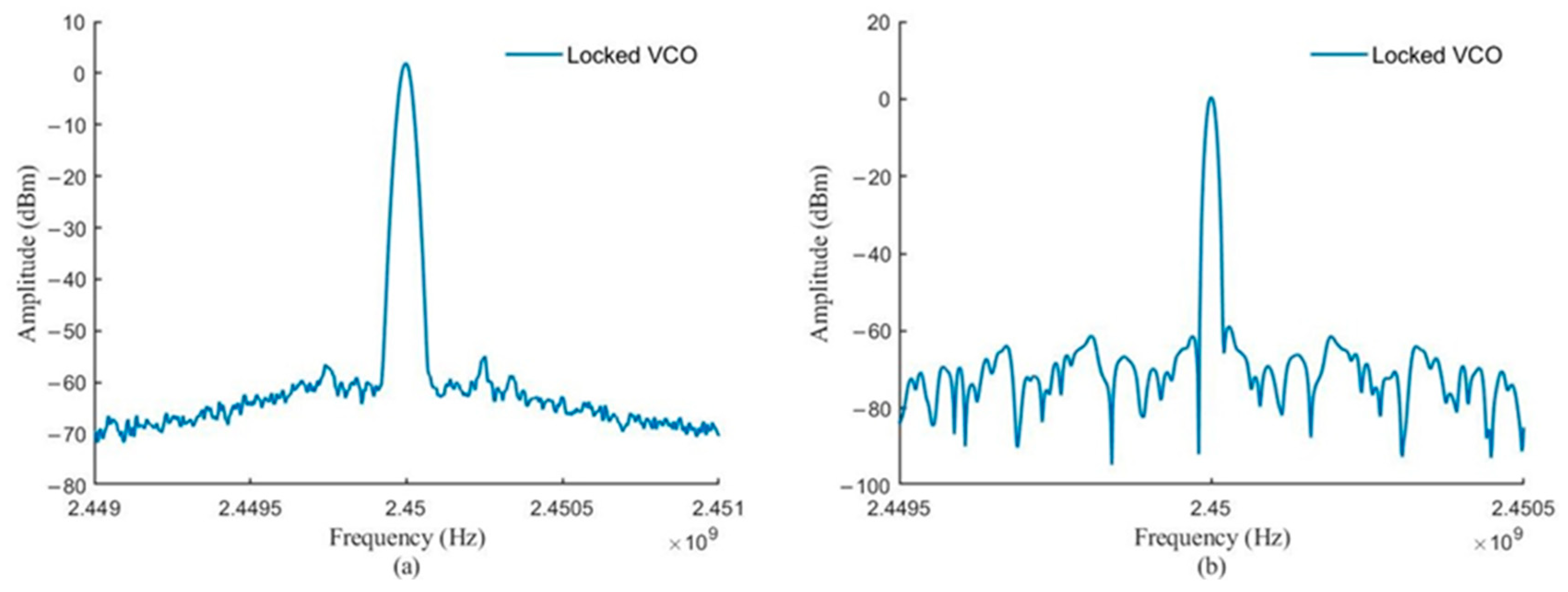
Figure 12 and
Figure 13 show the spectrum of the VCO output in broadband and narrowband. The VCO is locked to a unique frequency: the frequency of the external injection signal.
Figure 14 illustrates the phase noise of the output signal after locking. The phase noise is −113 dBc/Hz at 100 kHz offset of the center frequency, −121 dBc/Hz at 500 kHz offset, and −131 dBc/Hz at 1 MHz offset.
Figure 15 illustrates the phase noise of the output signal after locking. The locked VCO was measured using Agilent FSV. The phase noise is −15 dBc/Hz at 1 Hz offset of the center frequency, −65 dBc/Hz at 10 Hz offset, −100 dBc/Hz at 100 Hz offset, −125 dBc/Hz at 1 kHz offset, −132 dBc/Hz at 10 kHz offset, and−145 dBc/Hz at 100 kHz offset.
3.2. Cascading Injection-Locked VCO Arrays with Weak Reverse Coupling
Now, an injection-locked VCO without introducing additional circulators is implemented. We implement a VCO array where the phase shift of the VCO in this array depends only on the tuning voltage of this VCO (or the frequency of the output signal of free-running VCO). A cascaded injection-locked VCO array can satisfy this need. Equation (16) describes the phase performance for the VCO in the array.
is the phase for the
VCO,
is the injection ratio,
is the frequency of the free output signal for the
VCO,
and
is the frequency and phase of the external injection signal.
Under steady state, all VCOs are locked at the external injection frequency. Then,
Equation (18) shows that the phase difference between two adjacent VCO signals depends only on the quality factor of the VCO, the tuning voltage and the injection ratio.
To implement a cascade-locked VCO array is important. A simple idea is to let the injection signal of the VCO come from the output signal of the previous VCO in this array. However, in our proposed injection-locked VCO structure, the injection port will generate a signal output, and this higher power signal will generate reverse injection locking in the cascaded VCO array. This is not the desired result.
In order to keep the injection-locked array locked in the desired direction, reverse injection locking between VCOs must be eliminated. However, a situation where the reverse injection signal completely disappears does not exist, and a theoretically ideal cascaded injection-locked oscillator array cannot be achieved. However, we can make the power of the reverse injection signal as small as possible to minimize its effect on the VCO array. In reality, this would be a cascaded VCO array with weak reverse coupling;
Figure 16 shows a conceptual diagram of the VCO array.
To understand the effects of forward and reverse injected power on the VCO output phase, based on the analysis in
Section 2, an equation was developed to represent the output phase of a cascaded VCO array with weak reverse coupling.
where
,
is the phase for
VCO,
and
are the forward and reverse injection ratio,
is the frequency of the free output signal for
VCO,
and
are the frequency and phase of the external injection signal, and
denotes the phase shift of adjacent VCOs due to direct injection connection, which is called the coupling phase between the elements.
Under steady state, all VCOs are locked at the external injection frequency. Then,
Since the injection frequency is constant, the free oscillation frequency of a VCO can be changed. The phase difference between adjacent VCOs is determined by the injection ratio and the frequency of VCO. Its locking bandwidth can be expressed as
where
The locking bandwidth of the VCO under injection is not symmetrical with respect to the injection frequency, unlike the phenomenon of injection locking in a fixed frequency oscillator. The phase difference between the
VCO and the
VCO at steady state can be obtained by revising (20).
and
denote the forward and reverse injection power.
where
From (22), it can be seen that the phase difference between the VCO and the VCO at steady state not only depends on the intrinsic parameters of the VCO but also is affected by the phase difference between the VCO and the VCO; however, the regulation of all VCOs previous to the VCO does not affect the performance of VCOs after the VCO. denotes the ratio of forward injection power to reverse injection power, which is defined as the forward–reverse injection power ratio.
When the forward injection power is much greater than the reverse injection power, the effect of the phase difference change between the
VCO and the
VCO on the phase difference between the
VCO and the
VCO can be neglected. However, when the effect of the phase difference between the
VCO and the
VCO is not negligible, the effect will be transmitted between VCOs, and the phase difference between the
VCO and the
VCO can even have a strong effect on the phase difference between the 1st VCO and the 2nd VCO, which is illustrated in
Figure 17.
Now we consider how the phase noise of each stage of this VCO array can be improved. Based on the analysis in
Section 2, we can obtain the phase noise of the
VCO output signal.
and
represent the phase noise of the locked and free states of the
VCO.
represents the phase noise of the externally injected signal.
where
Then, we make a simple revision of (23):
where
Further, the phase noise of each VCO output signal in the N-stage VCO array can be obtained by (24)
where
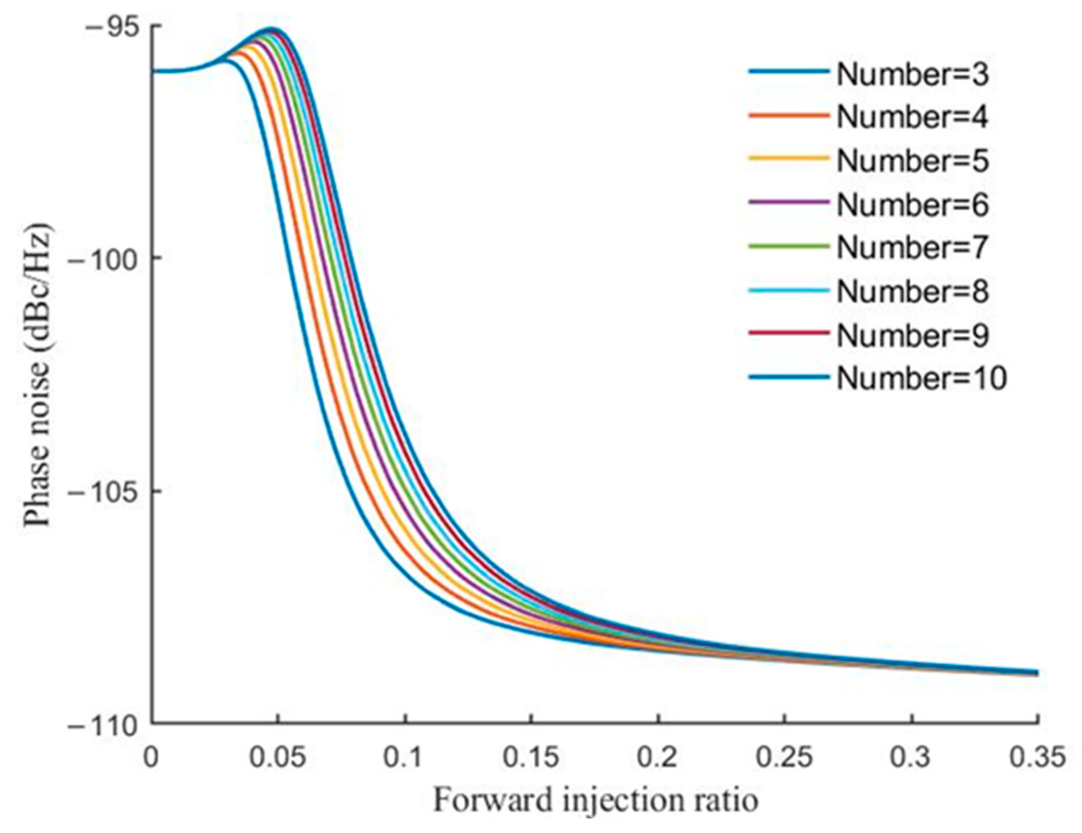
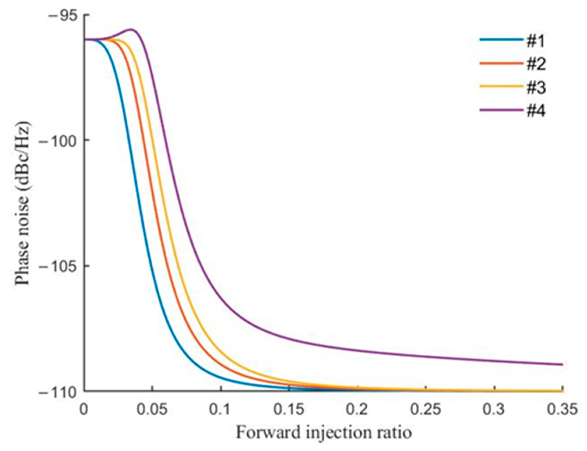
and represent the phase noise of the VCO signal in the locked and free-running states, and is the transformation matrix of the two, which is a function of the injection ratio and the phase difference of the adjacent VCOs. When we know the phase noise of each VCO in this array under free operation and the phase noise of the injected source, we can predict the phase noise of each locked VCO in this array at different phase shifts’ output signal of other VCOs. We find that the phase noise improves with increasing forward injection ratio, and the phase noise of the VCO signal does not deteriorate rapidly with increasing the number of VCOs in the array for greater forward injection ratios.
Figure 18 shows the variation of the phase noise of each VCO with the forward injection ratio for an array of four stages, and
Figure 19 shows the variation of the phase noise of the last VCO signal with the forward injection ratio for a different number of elements of the VCO array. We need a high forward injection ratio and a high forward-to-reverse injection power ratio in order to guarantee the phase noise of the output signal and to reduce the impact of the next VCO phase regulation on the output phase of the previous VCO. Based on the above analysis, a cascaded injection-locked VCO array with weak reverse coupling is designed for beam scanning.
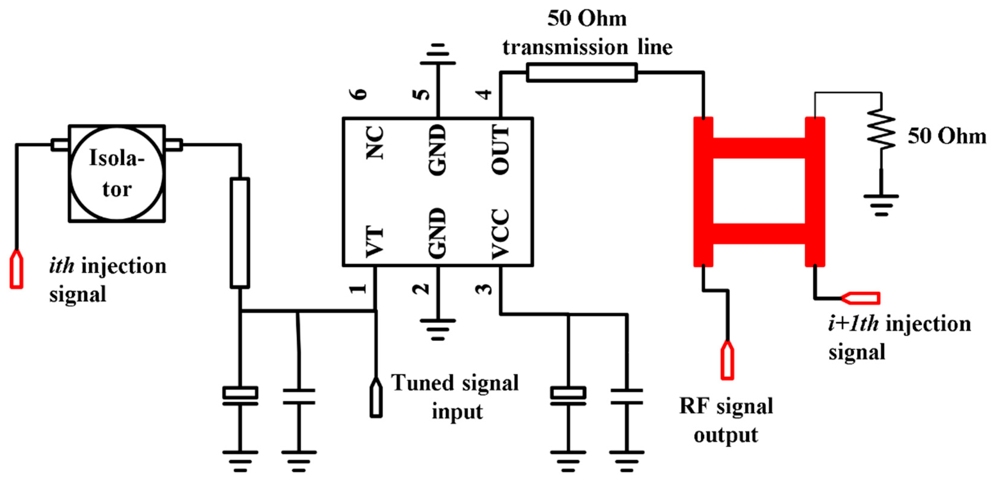
Figure 20 shows the schematic of the elements in the VCO array.
Figure 21 shows the physical diagram of the VCO, which operates at 2.45 GHz. The dielectric substrate is FR4, with a thickness of 1 mm. The signal at the output port of the VCO provides the external injection signal of the next VCO by plugging into the coupler at this port (used to provide a greater forward injection ratio). The magnitude of this signal power is determined by the coupling degree of the coupler, and the forward injection ratio of this VCO array is determined when a well-designed coupler is connected to the circuit. Ignoring the additional insertion loss (about 0.3 dB) caused by the connector of this port, the forward injection ratio of the VCO array is equal to the coupling degree of the coupler. The VT port of the VCO is connected to an isolator to reduce the power of the reverse injection signal.
It is known that the output power of this chip at the VT port is reduced by 3 dB compared to the output port. Thus, the reverse injection ratio of this VCO array can be expressed as C+D+3 dB, where D represents the isolation degree of the isolator, and C represents the coupling degree of the coupler. Then, the forward–reverse injection power ratio of the VCO array is D+3 dB. In this design, the coupling degree of the designed coupler is 13 dB at 2.45 GHz, and the isolation degree of the used isolator is 27 dB at 2.45 GHz.
Figure 22 shows the physical diagram of the 4-stage VCO array,
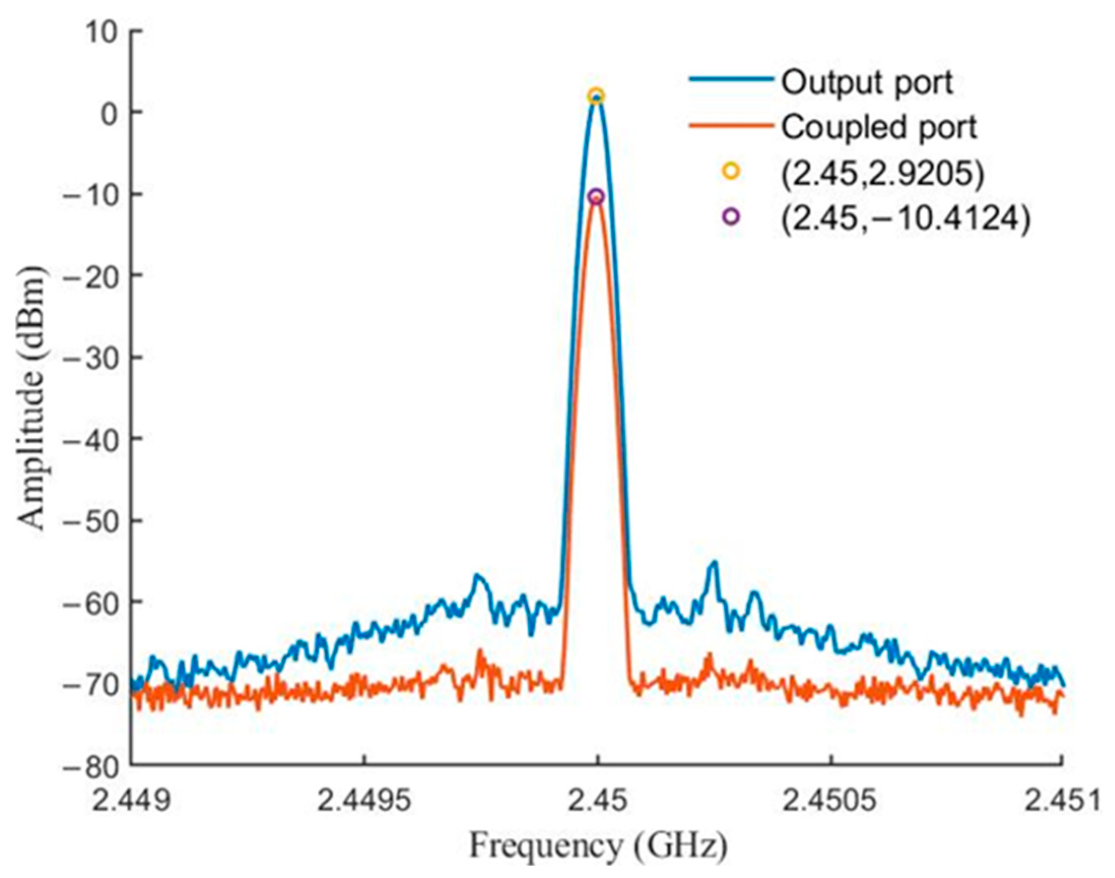
Figure 23 shows the spectrum of the output signal of the coupling port after the output port of the locked VCO is connected to the coupler, and it can be seen that the forward injection ratio of the VCO array is 13 dB at 2.45 GHz;
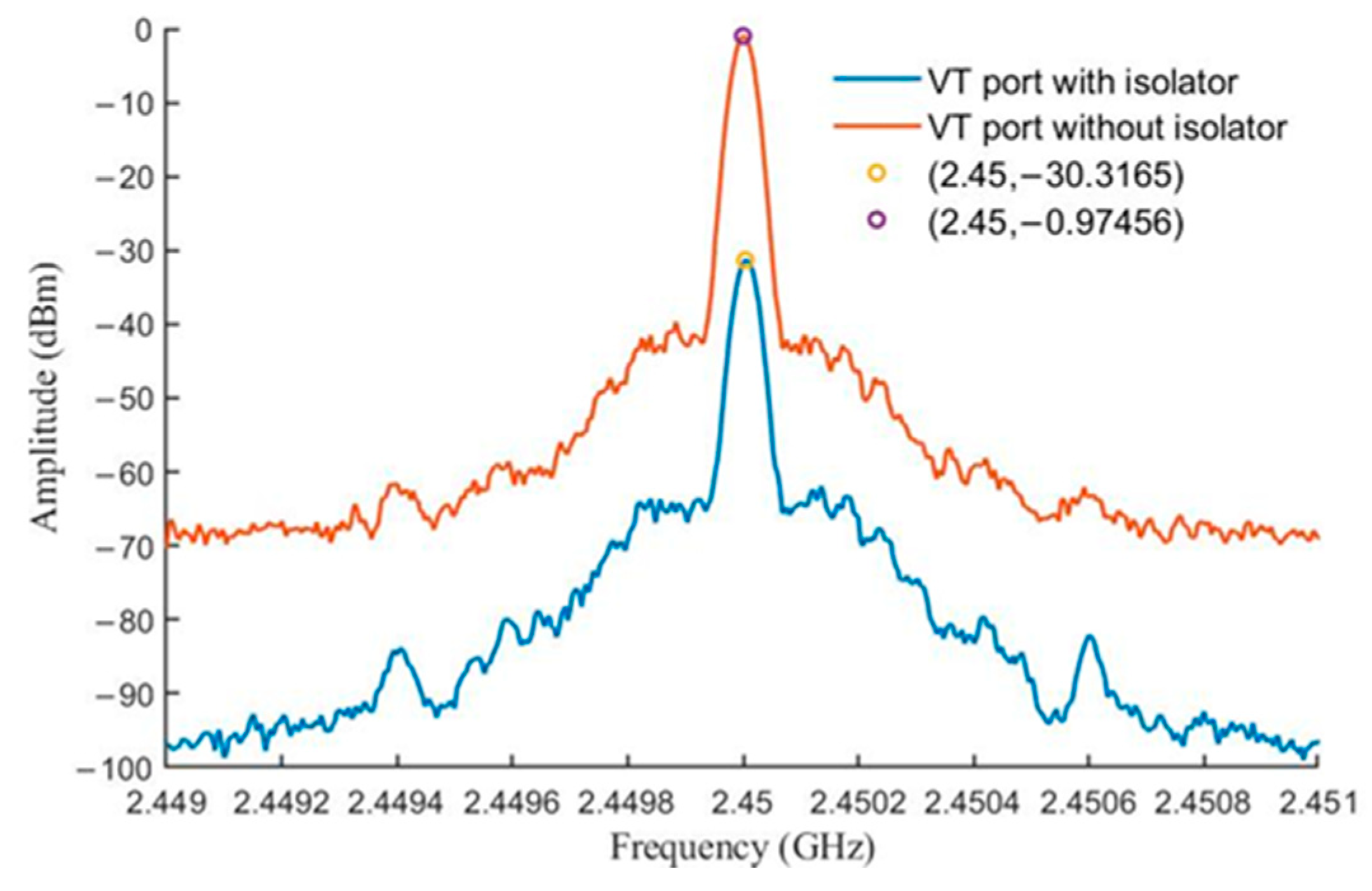
Figure 24 illustrates the spectrum of the signal output from the injection port, when the VT port of the locked VCO is connected to an isolator, and it can be seen that the forward–reverse injection power ratio of the VCO array is 30 dB at 2.45 GHz.
3.3. A Continuous Full 360° Phase Shift Array
Phase shifter circuits include vector sum [
21], reflective [
22] and switching [
23]. The phase control characteristics of any type of phase shifter are not linear. The nonlinearity of the phase control characteristics leads to the degradation of the antenna directionality in phased array applications.
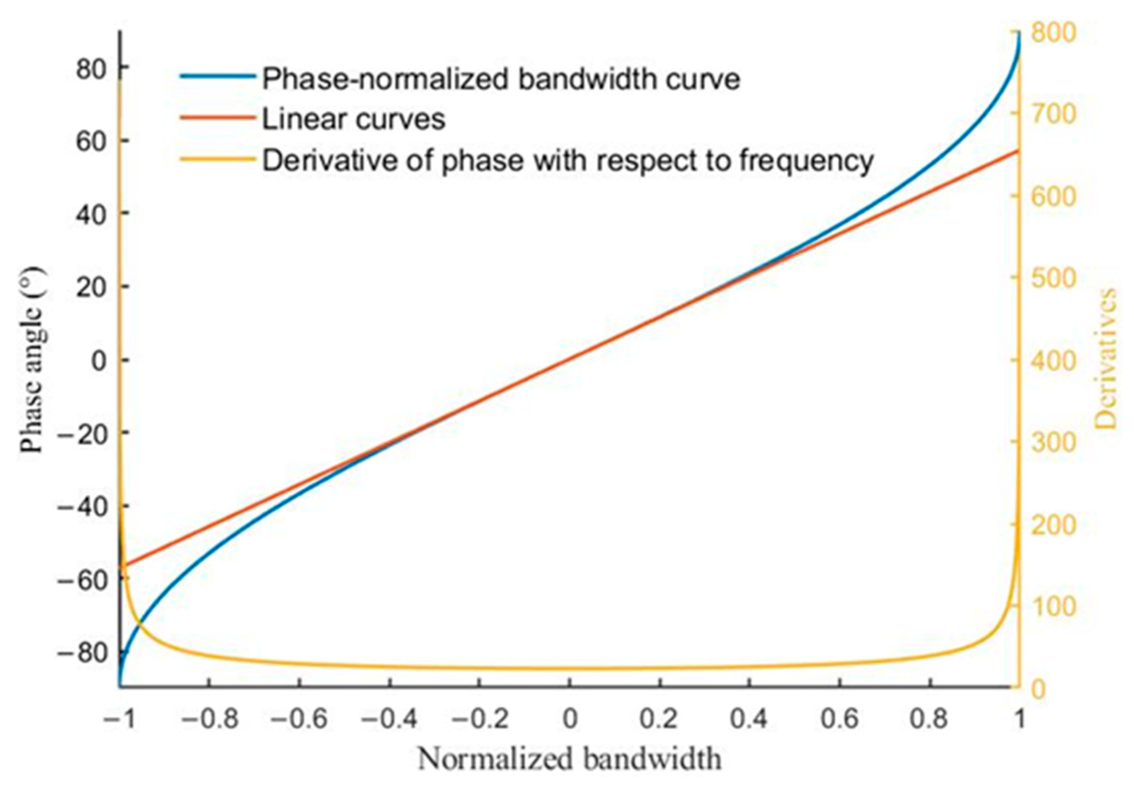
However, the phase difference between the injected locked VCO output signal and the injected signal shows good linearity over a certain tuning range, as shown in
Figure 25. the phase difference range with good linearity is less than 180 degrees. The small phase range of the output signal will result in a very narrow scanning angle range of the antenna array. Therefore, a digital phase shifter between adjacent VCOs is considered to widen the phase difference between adjacent output signals.
Phase shifting is done in three steps. Firstly, the digital phase shifter is used to achieve wider angle scanning. Then, the phase difference between adjacent VCO signals is adjusted by adjusting the free output frequency of the VCO. Finally, the phase difference reaches the desired value.
Theoretically, the output phase of an injection-locked oscillator can range from −90° to +90° [
24]. If the phase frequency curve is linear over this range, only a small amount of the phase shifter (180°) is needed to achieve a 360° adjustable phase output. However, this is difficult.
Figure 25 shows that the linear adjustment range of the phase can vary with the injection ratio of 0.15.
The connection of each VCO in the circuit will result in a different initial phase. When the center frequency of the VCO is equal to the frequency of the injected signal, the phase difference between adjacent VCOs is not zero. As the phase difference between the outputs of each adjacent VCO is not the same at this time, we need a certain phase shift to offset this angle.
When a phase shifter is inserted, the forward power of the VCO array will be reduced, which means that the available linear region will be reduced again. The phase noise of the signal will deteriorate as the phase difference of the VCO increases. Therefore, when a phase shifter with poor insertion loss performance is considered, a 3-bit digital phase shifter is required. After inserting the phase shifter, there is no change in the forward-to-reverse injection power ratio, which means there is no change in the effect of the next VCO tuning on the phase of the previous VCO. There is no change in the output signal power from the oscillator.
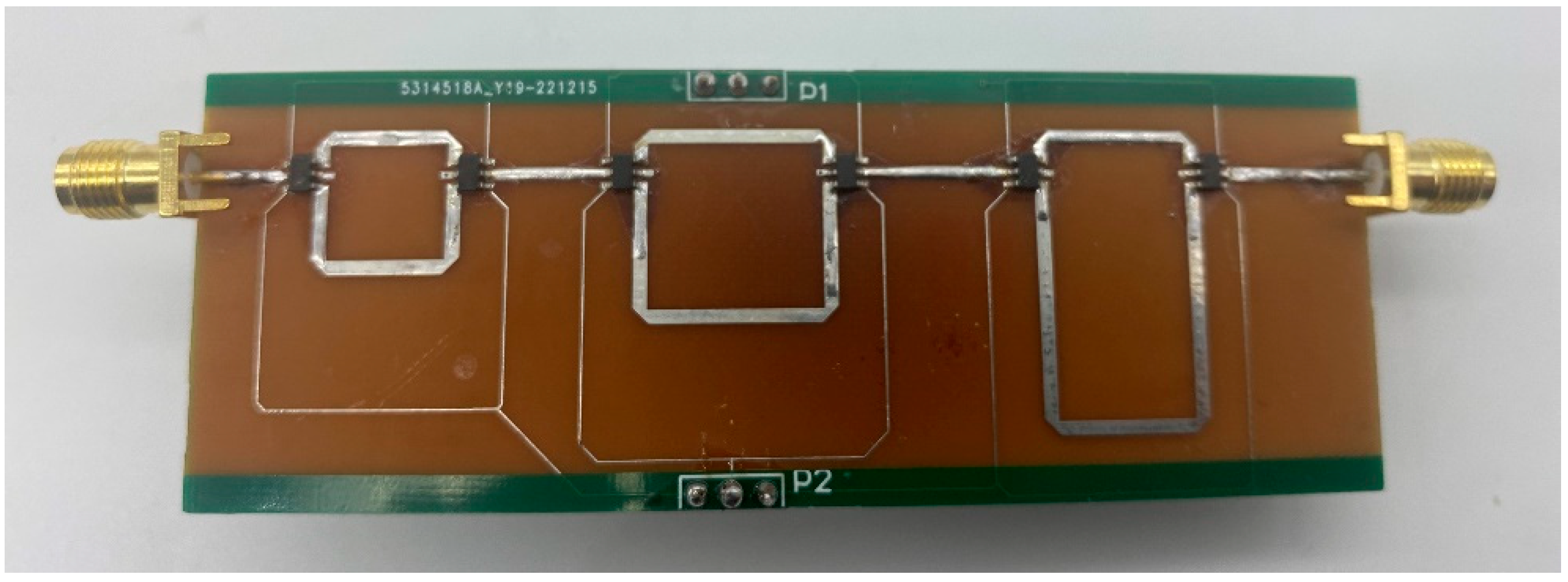
Figure 26 shows the physical diagram of the 3-bit phase shifter with FR4 substrate and 0.6 mm thickness, using HMC545AE to realize the control of the digital phase shifter.
Figure 27 shows the physical diagram of the digital phase shifter connected between adjacent VCOs. At different phase shifts, the insertion loss of the phase shifter does not change significantly. If the phase shifter performs poorly, such as having an inaccurate phase shift angle, we can also compensate using the phase of the locked VCO, which can be adjusted by changing the tuning voltage of the VCO. This determines the phase difference between adjacent VCO output signals.
4. Results
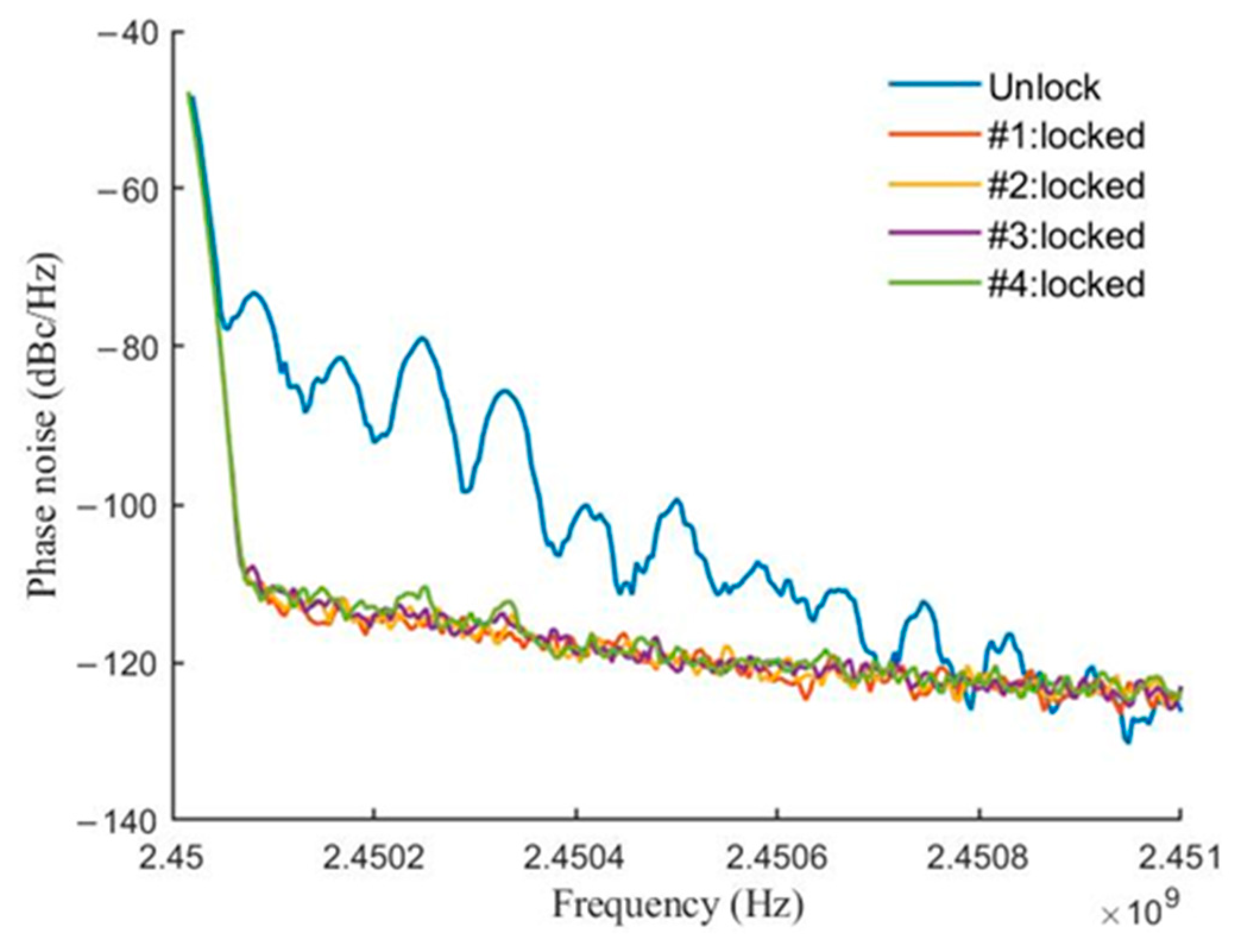
In order to verify the phase adjustment capability of our proposed VCO array, we use the above structure to form a one-dimensional linear VCO array with four array elements. At the same time, an antenna is connected to the output port of each VCO. By adjusting the direct phase difference of the array VCO, the phase change of the main lobe of the antenna radiation pattern can be realized. A phased array consisting of four VCOs radiating different modes was used to demonstrate beam scanning. The array was prepared on a substrate of FR4 material with a thickness of 1 mm. Under cascading injection locking, the output signal of the VCOs at each stage was measured by a spectrometer, as shown in
Figure 28. The blue lines indicate that the VCO is not locked. Each level of the cascaded VCO array is injection-locked under external signal injection. Under the condition of a large forward injection ratio, the phase noise of each stage VCO behaves well and is approximately equal. Nevertheless, the green lines represent relatively poor phase behavior. It can be observed that the phase noise of the signal gradually deteriorates.
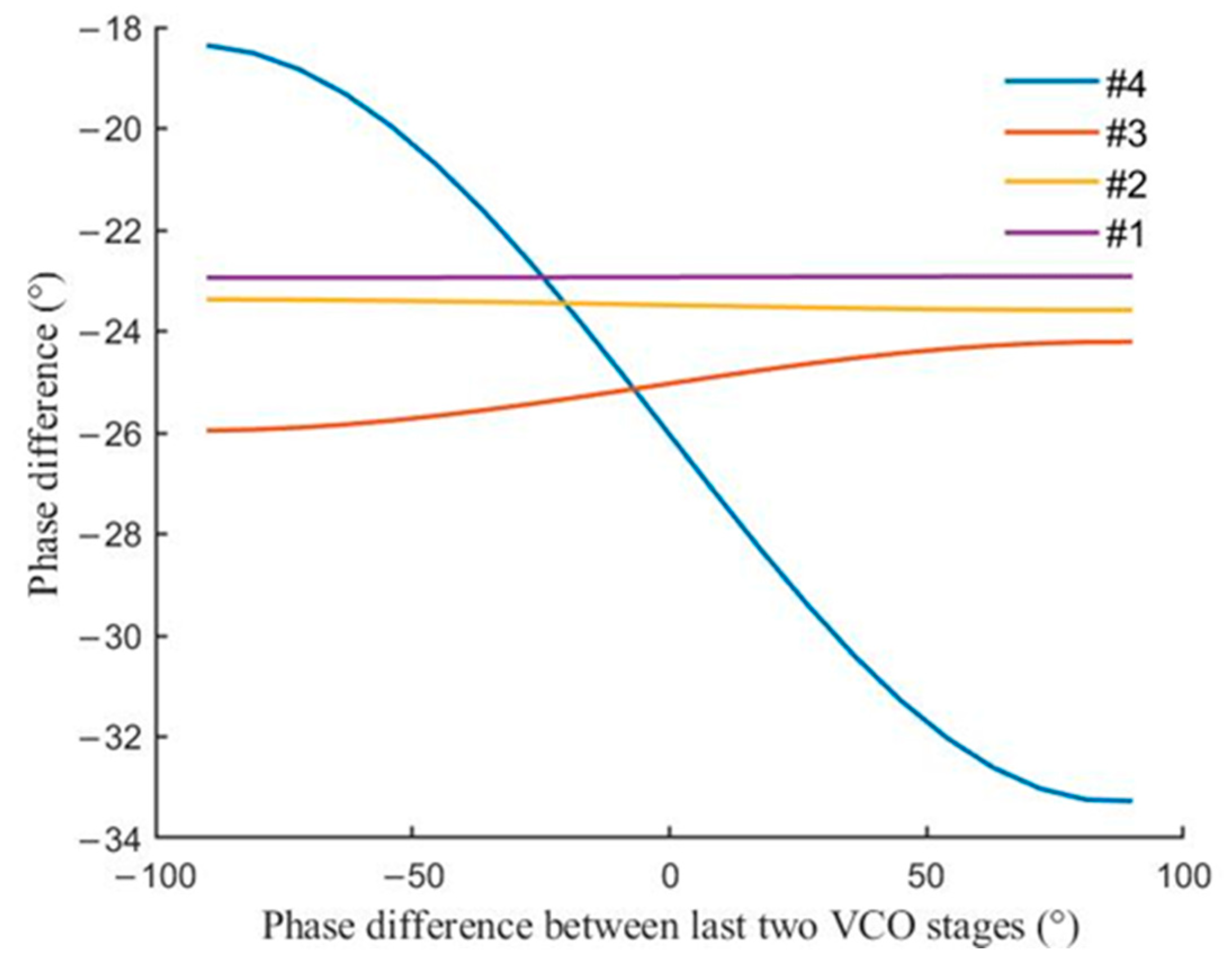
The phase difference of the VCO output signal between stages is obtained through the discriminator, and the change in phase difference of each stage is obtained by adjusting the frequency of the fourth stage VCO, as shown in
Figure 29. The change of frequency of the output signal of the last stage affects the output phase of the signal, while the phase difference of each stage changes because of the presence of the reverse injection ratio. It can be observed in the figure that the phase change of the fourth stage VCO in the locking range does not produce a significant change to the third stage VCO, due to the array having a small reverse injection ratio. Under these conditions, each stage of phase regulation can be considered independent. In other words, the phase regulation of each VCO stage is affected by the tuning voltage of the VCO stage. The further away from the last level of the VCO, the weaker the effect of the phase difference of the output signal.
The proposed VCO array is designed to be used in phased array beam scanning. In order to show the good phase shift characteristics of the VCO array, the antenna array, shown in
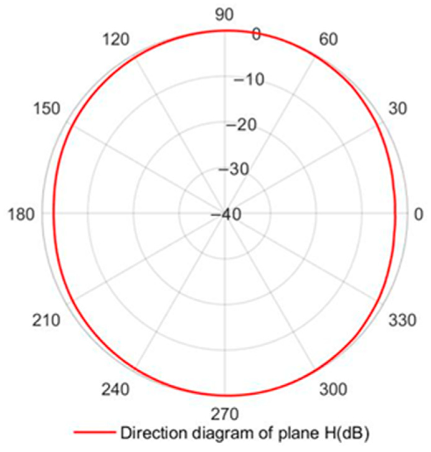
Figure 30, is connected to the output end of the VCO array. The antenna array consists of a dipole antenna. This antenna has good omnidirectivity.
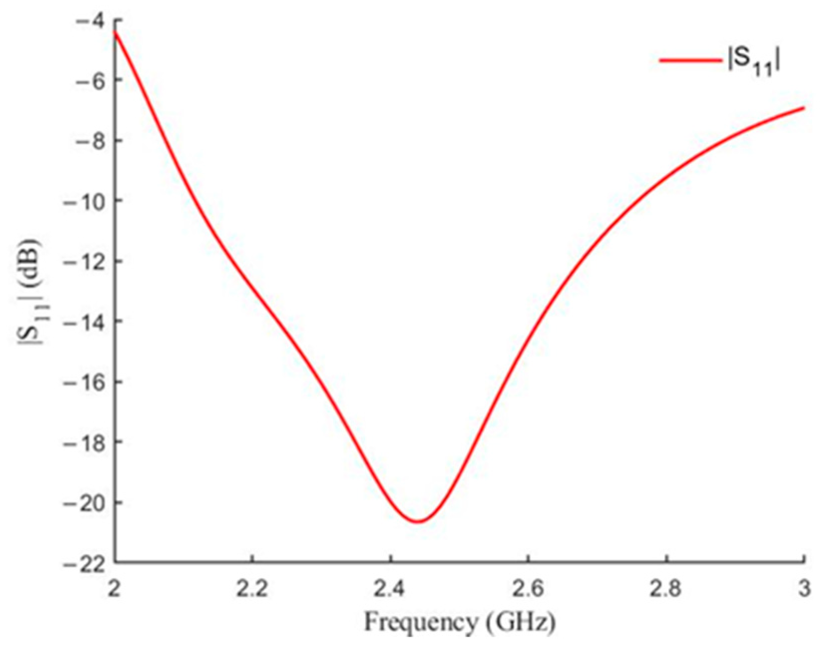
Figure 31 shows the S parameter of the antenna unit, which has a small reflected power at the operating frequency of 2.45 GHz.
Figure 32 shows the normalized orientation diagram of the array unit at the operating frequency. Since the orientation pattern of the antenna array is determined by the array factor and the orientation pattern of the array element, the influence of the antenna element orientation pattern on the array antenna orientation pattern can be ignored as much as possible by adopting the omnidirectional antenna, so as to verify the phase shifting characteristics of the VCO array more obviously.
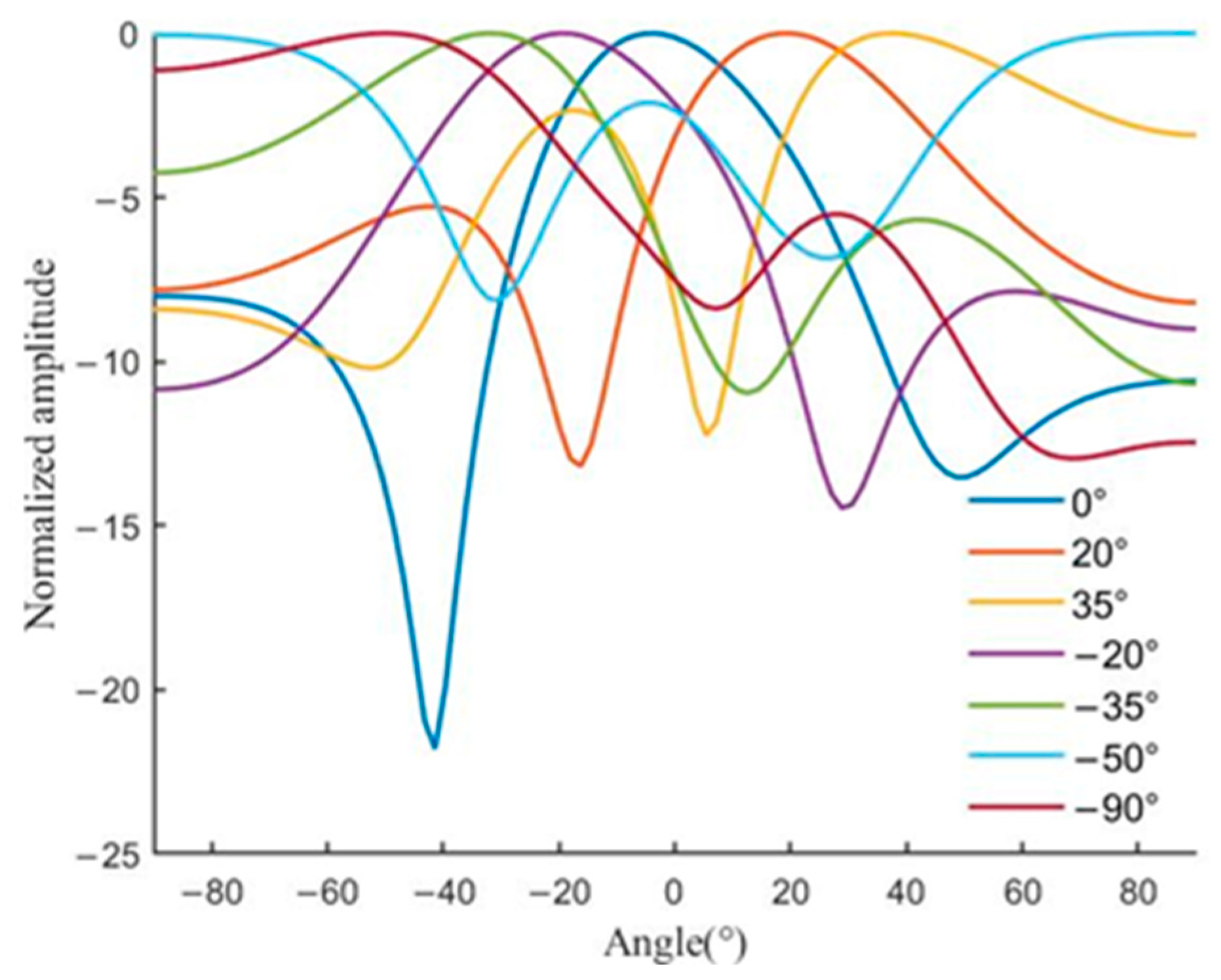
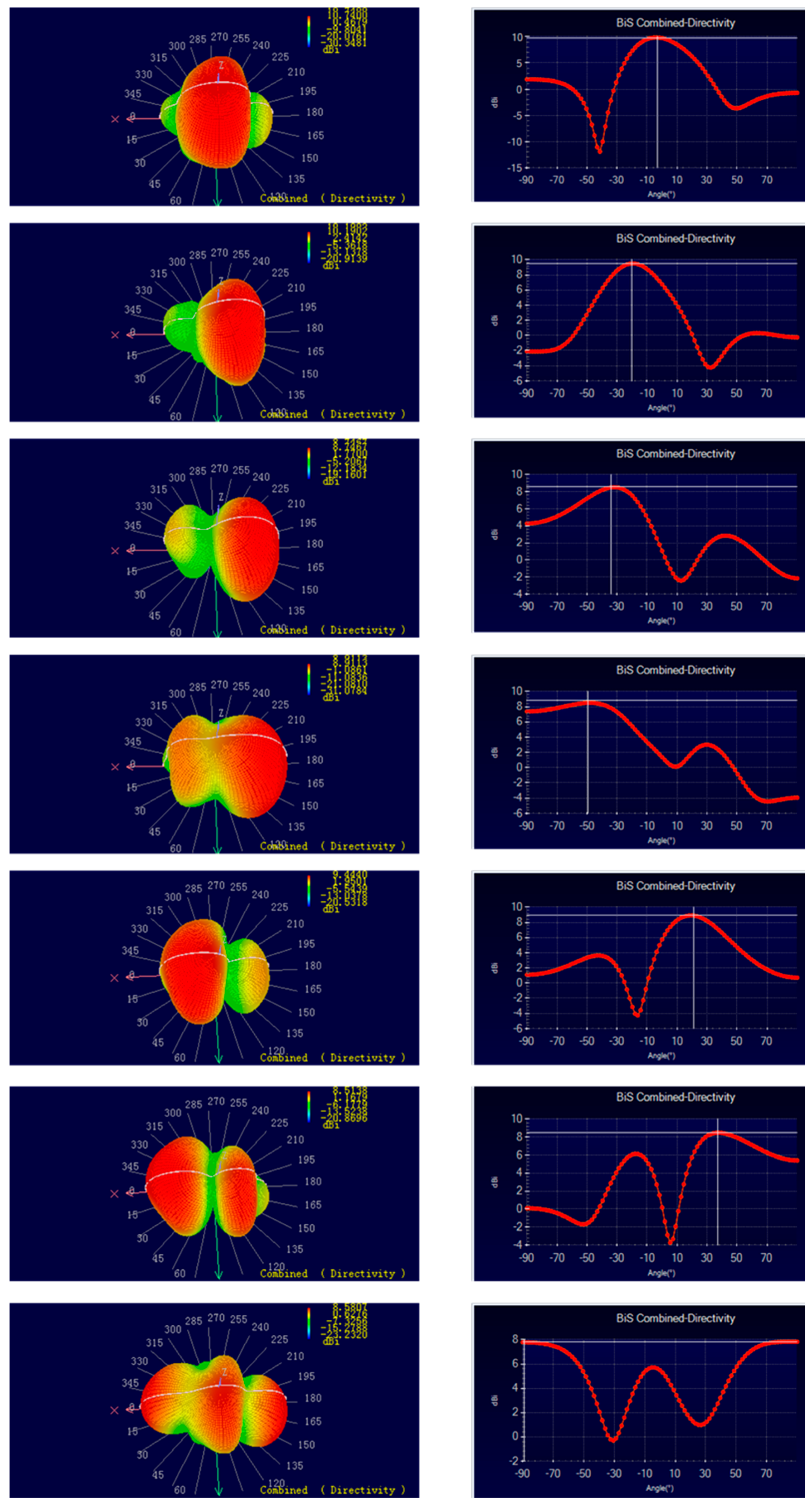
Finally, beam scanning was demonstrated using an active phased array with different modes of radiation. The observed beam scan ranges from −90° to +90° (
Figure 33). The maximum beam scanning angle is 180°, which is very close to the theoretical prediction of 180°, when the antenna elements are spaced at half wavelength distance. In the measurement, the antenna array is placed on the XOY plane and parallel to the
Y-axis, as shown in
Figure 34, which details the 3D orientation of the beam scanning while the orientation diagram of the H-plane is intercepted. The variation of the phase angle of the main lobe in the antenna array pattern can be clearly observed. There is a gain drop when the beam scanning angle increases. Compared with the theoretical model, the measured directional graph has some distortion, and the directional graph has a large sidelobe. The reason for this may be the mutual coupling between the antennas and the lack of measurement accuracy in detecting the main beam direction. When compared to the recently published design in
Table 1, it can be seen that the proposed cascaded injection-locked VCO array has the characteristics of easy expansion, continuous phase adjustment and wide beam scanning range, making it suitable for phased array beam scanning.
