1. Introduction
In radio-frequency (RF) circuits, the RF devices operate under the rule of electromagnetic fields. As a consequence, circuit theory is generally insufficient for analyzing RF devices. Instead, a more rigorous theory, i.e., electromagnetic field theory, must be invoked to study RF devices. Advanced electromagnetic simulation tools help RF engineers to design successful RF chips and accelerate the product design process by evaluating the design performance, reducing trial and error costs, improving design efficiency, optimizing the design configuration, and so on. Efficient electromagnetic computation is an essential engine of all electromagnetic simulation tools.
Due to the diversity and complexity of electromagnetic field problems that need to be solved in practical engineering, a variety of numerical methods have been developed in computational electromagnetics [
1,
2,
3,
4,
5,
6]. In these algorithms, the numerical solution of Maxwell’s equations usually involves meshing or discretization, in which a continuous solution domain is discretized into a finite number of elements and the accuracy of computational results is dependent on the element size. After meshing or discretization, Maxwell’s equations are reduced to a linear matrix system. Better accuracy can be obtained by increasing the mesh density. A finer mesh usually leads to higher accuracy but requires longer computational time and larger memory consumption. At the limit, where the mesh becomes infinitely dense, theoretically, the numerical solution should converge to the exact solution of Maxwell’s equations [
7,
8,
9]. In practice, however, computing resources are always limited. Hence, a mesh scheme needs to be developed for attaining a proper mesh on which an accurate solution can be obtained with the minimum consumption of computing resources. In the case of the same computational method, the mesh quality is the most critical factor for determining computational accuracy and efficiency.
There have been many efforts in developing optimal mesh generation schemes for electromagnetic computations. For example, the mesh improvement of the boundary integral method, similar to the traditional finite element method, can have a variety of approaches, such as h-, p-, and r-type schemes. The h-type scheme approximates the exact solution by continuously making the mesh denser while keeping the element order unchanged [
10]. The p-type scheme improves the computational results by increasing the lowest order of the elements without changing the meshing of the structure [
11]. The r-type scheme reduces the solution errors by rearranging the mesh without changing the number of elements [
12].
In addition, there are several forms of hybrid methods. The h-type scheme has good convergence properties for functions with singular points, but the mesh refinement may significantly increase the number of unknowns. Although the p-type scheme does not increase the number of elements, it does increase the order of elements and, thus, the solution complexity. In particular, for the integrated circuits that are usually planar structured, low-order basis functions are more effective. Although the r-type scheme also does not increase the number of elements, rearranging the mesh alone does not guarantee the solution convergence, and, thus, it generally requires mixing the h-type scheme to attain a convergent solution.
The iteration process strongly depends on the efficiency of mesh refinement, in which new grids (elements) are repeatedly added, and the computations are carried out over each refined mesh repeatedly, resulting in a large amount of time consumption. In [
13], the hp-type adaptive finite element method was studied in three-dimensional electromagnetic computation. The hp-type adaptive finite element method can effectively improve the solution accuracy. However, the meshes studied in [
13] are mainly structured ones, and the adaptive mesh refinement algorithm is aimed at the cuboid meshes only, which is hardly applied to complex and irregular structures. In [
14], the dual error estimation weighting method (DEW) was introduced for adaptive mesh refinement control, which can achieve a highly accurate solution. However, the approximate gradient term used in the gradient recovery method must be used in a uniformly conductive region, and otherwise, the error is larger. In addition, the dual residual weighting method (DRW) is much more complex, and thus hardly used in three-dimensional problems. In [
15], the unstructured meshing program “Triangle” was reported to create two-dimensional geoelectric models and generate adaptive finite element meshes, to which most studies of adaptive finite element meshing algorithms have been applied. In an analysis of solid and structural mechanics [
16], the strain gradient was utilized to analyze local solution characteristics in stress-concentrated and rapidly changing strain regions [
12] which can provide a theoretical basis for the mesh refinement but could not guarantee convergence in any form of mesh generation.
In this work, an adaptive mesh generation technique for efficient electromagnetic computation in RFIC designs is developed. According to the characteristics of RFICs, the problems of strong coupling, edge effect, and large-scale via arrays, which plague the efficiency of electromagnetic computation, are paid special attention. In RFICs, some metal structures (e.g., capacitors) are very closely arranged. When the gap between two metals is very small, the mesh size must be generally comparable to the gap for achieving good accuracy which leads to a large number of small elements and, thus, deteriorates the computational efficiency. A projection-based mesh scheme is herein introduced to effectively treat and subdivide very closed-arranged structures which can greatly reduce the number of small elements yet maintain good accuracy. At high frequencies, the current distribution most likely concentrates at the edges of metals. To reflect this edge effect, an adaptive edge mesh scheme is applied to generate finer meshes at metal edges whereas coarser meshes are used in the middle of metals. In addition, via arrays that are commonly present in RFICs. Direct meshing of these tiny metals may lead to a large number of elements or unknowns which could significantly deteriorate the computational efficiency and consume a great deal of memory resources. A scheme of aggregating these tiny metals is introduced to improve computational efficiency yet keep good computational accuracy.
2. Mesh Schemes
For EM simulation in RFICs, the problem can be formulated in terms of the mixed-potential integral equation (MPIE) [
17,
18]
where
,
S,
,
,
,
, and
are the current density, closed metal surface, angular frequency, permeability in vacuum, permittivity in vacuum, observation point, and source point, respectively. In addition,
and
are the dyadic and scalar multilayered dielectric medium Green’s functions [
19], respectively. Since the effects of multilayered dielectric medium are included in the Green’s functions, only the metal structures in RFICs need to be meshed.
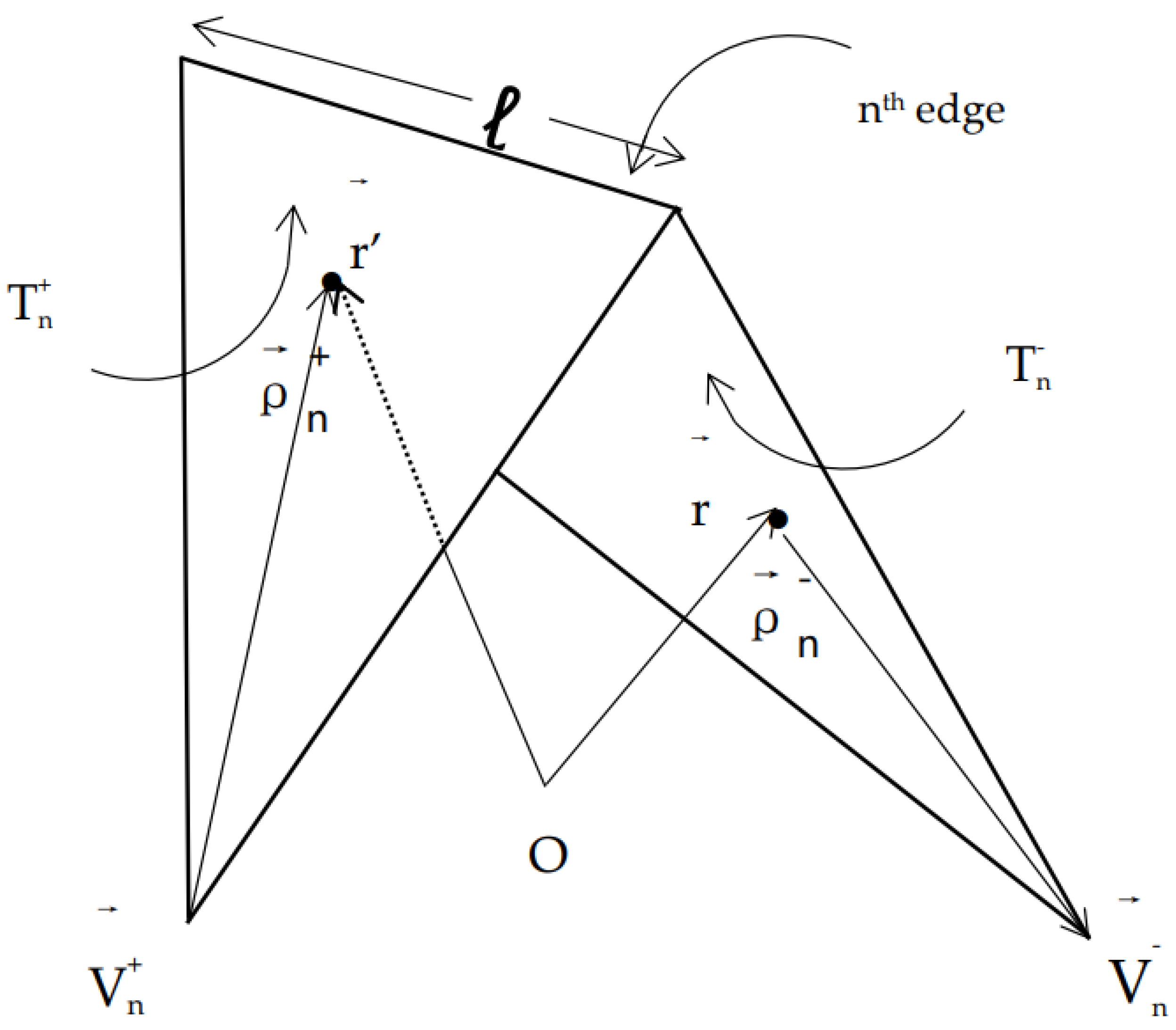
The surface current is expanded by virtue of the zero-th divergence conforming basis (DCB) functions (e.g., triangular mesh-based RWG [
20] as shown in
Figure 1), viz.,
where
Then, the Galerkin procedure is applied to (1) to generate a method of moment (MoM) matrix equation, viz.,
where
N is the number of basis functions. The entries of the impedance matrix
and excitation vector
are calculated as
and
- (a)
Projection scheme
In RFICs, metals, such as metal structures in flat plates or finger capacitors that are very closely arranged have strong electromagnetic coupling due to the proximity effect, particularly between two very closely nearby metal surfaces. In order to accurately model such strong electromagnetic coupling, it requires a very high density of meshes in a brute-force approach. Such a brute-force approach could result in too many elements or unknowns which consumes too much memory resource and CPU time and is usually intolerable in many cases.
Consider the numerical evaluations of (5) and (6), in which the Gaussian integration is generally used. By substituting (3) into (5) and using the Gaussian integration, each of the items in the (5) related to
can be expressed as
and the component associated with
can be expressed as:
where
and
are in the “+” triangles of RWG
i and
j, respectively, NG represents the number of Gaussian sampling points,
and
are the sampling points on the field and source triangles, respectively, and
and
denote the corresponding Gaussian integration weights to the sampling points on the field and source triangles, respectively.
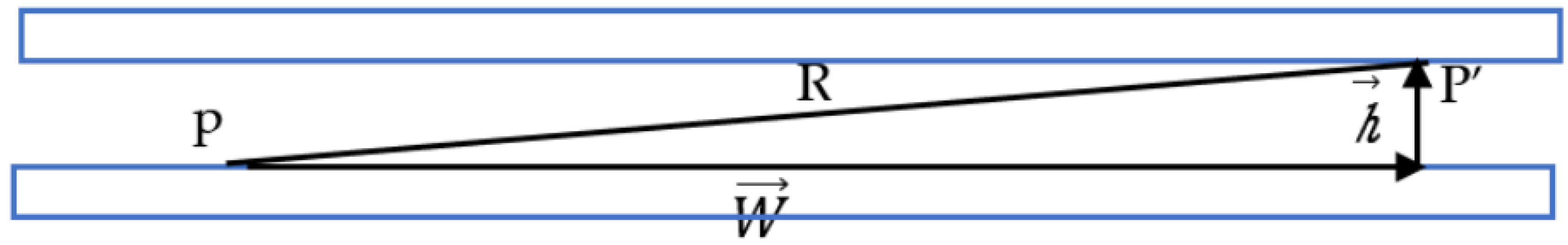
Consider the case that two metal surfaces are very closely apart, in which the field and source triangles may still be very close even though they locate in different metal surfaces as shown in
Figure 2. In this case, some pseudo-singularity in (7) and (8) needs to be well treated. Without loss of generality, consider the free-space Green’s function:
where
,
is the distance vector between two metal surfaces, and
is the offset vector between the field and source points.
Since h is very small, there is a pseudo-singularity in (9) which behaves as 1/R or 1/h. When the distance between two metal surfaces is very small, the coupling between them is very strong. In evaluations of (7) and (8), the pseudo-singularity of 1/h plays an important role since 1/h becomes very large as h is very small and may contribute the most to the coupling between the two metal surfaces. However, when the offset W is much greater than the gap h, the value of 1/R becomes much larger than the value of 1/h. As a consequence, the Green’s function becomes too small to reflect the strong coupling between the two metal surfaces. In order to accurately capture such a pseudo-singularity behavior in the Gaussian integration, the offset of two nearby sampling field and source points in the Gaussian integration must be smaller than h which may require very fine mesh and, thus, result in too many unknowns in the numerical computation.
Alternatively, a projection-based mesh scheme can be used. Specifically, one can first identify the aligning areas between these two metal surfaces that are closely apart. Then, the two aligned areas are meshed in the same manner through a projection from one metal surface to the other metal surface, so that there is no offset between two meshes along the metal surfaces.
With the projection-based mesh scheme, the triangular elements between the metal surfaces are well aligned, and so do the Gaussian sampling points on these triangular elements. As a consequence, the Green’s function computed on the field and source points which locate at the aligned Gaussian sampling points, can take well account of pseudo-singularity 1/h regardless the size of the triangular elements. Therefore, accurate numerical integration in (7) and (8) can be achieved without requiring very fine mesh.
The projection-based mesh scheme can be applied to on-chip parallel-plate capacitors, in which the gap between two metal plates is usually designed to be very small in order to increase the capacitance. For multilayered finger capacitors, the gap between two fingers is also designed to be very small to achieve large capacitance, and, thus, the projection-based mesh scheme is also required to mesh multiple fingers in multiple layers.
The projection algorithm works as follows:
Check whether the distance between metal layers satisfies the proximity condition. If so, take the geometries on the metal layers that need to be projected (L1, L2, …, Ln) and perform a Boolean AND operation to obtain the common part A.
Use “triangle” to generate a triangular mesh for A and record the edge points P.
Subtract A from (L1, L2, …, Ln) to obtain the shapes (S1, S2, …, Sn) and place P on (S1, S2, …, Sn).
Triangulate (S1, S2, …, Sn) with P while enforcing that the edges do not increase the number of points to ensure element alignment.
The resulting mesh consists of the elements obtained by triangulating (S1, S2, …, Sn) with P and the elements obtained by triangulating A.
- (b)
Edge refinement
In high-frequency circuits, electrical current changes rapidly and distributes unevenly on cross-sections of metal lines. In general, the current most likely concentrates at the edges whereas is relatively flat in the middle areas of metal lines. To effectively characterize the edge concentration, it is highly desirable to have finer meshes at the edges.
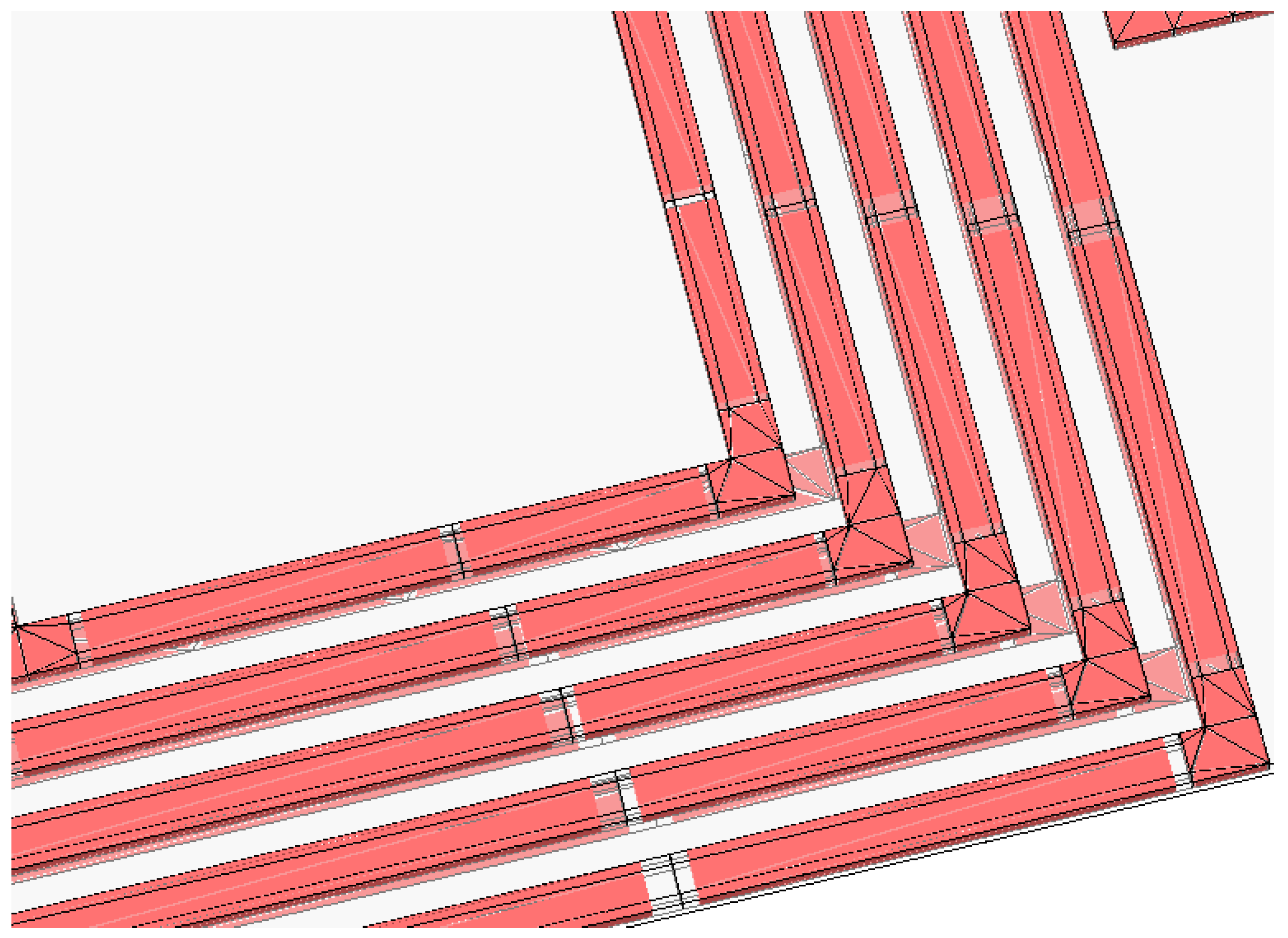
In general, the metal traces in integrated circuits can be refined at the edges proportionally. As shown in
Figure 3, for example, the sidewalls of metal traces are subdivided into three segments according to the ratio of 0.2:0.6:0.2, whereas the top and bottom surfaces of metal traces are subdivided into four segments according to the ratio of 0.2:0.3:0.3:0.2.
In general, rectangular meshes are used in the middle areas of metal traces whereas triangular meshes are employed at the corners of metal traces. With mesh edge refinement, the current can be better characterized, and, thus, more accurate numerical results can be obtained with fewer unknowns.
- (c)
Via aggregation
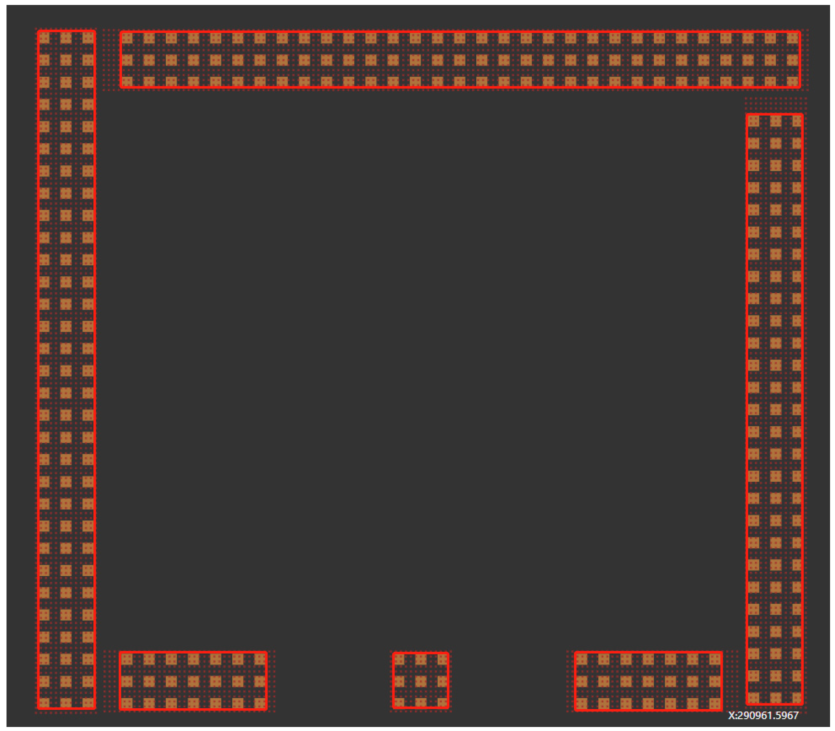
There are sometimes many small metal objects (such as via arrays) in integrated circuits. These metal objects are huge in number, but their structures are very simple, mainly playing the role of connecting upper and lower metal layers. If they are processed one by one, they could consume a great deal of computer resources in both CPU time and memory storage. Nevertheless, the small elements from these small metal objects and the large elements from RF devices can also cause a wide disparity of geometrical scales which may cause numerical instability.
During the mesh generation, it is, thus, necessary to identify the groups of vias and aggregate each of them into a large via, in which the large aggregated vias should keep the same electrical connections as the original vias do. Fortunately, these small via arrays are regularly arranged in integrated circuits. In many cases, their size, shape, and spacing are exactly the same, and, thus, it can be readily identified whether they belong to the same group of via arrays (as shown in
Figure 4).
The equivalent conductivity of a large aggregated via can be simply modeled as the mean of the conductivities across the entire cross-section that contains the original via array. The large aggregated vias are then meshed, by which the number of unknowns can be greatly reduced, and the wide disparity of geometrical scales can be well resolved. The via aggregation can greatly speed up the electromagnetic computation yet virtually without compromising the result accuracy.
3. Examples and Validation
In this section, some examples are included to validate the mesh schemes proposed in the preceding section. The standard mesh algorithm is a force-brute approach, in which the mesh is most likely to be uniformly distributed without any optimization to on-chip structures. Moreover, in general, the rectangular mesh is used for metal paths and metal sidewalls, while the triangular mesh is employed for all other metal parts. The reference solution is obtained by iteratively refining the mesh until the result is completely converged, in which this final converged result is used as a reference for comparison. Herein, the space in which no dielectric medium is specified is assumed to be air for computations of the multilayered dielectric Green’s functions. The hardware configuration of the server used in all the following simulations is as follows: Intel(R) Xeon(R) CPU E7-4830 v4 @ 2.00 GHz 14 Core × 4 400 G RAM Threads 4.
- (d)
Projection scheme
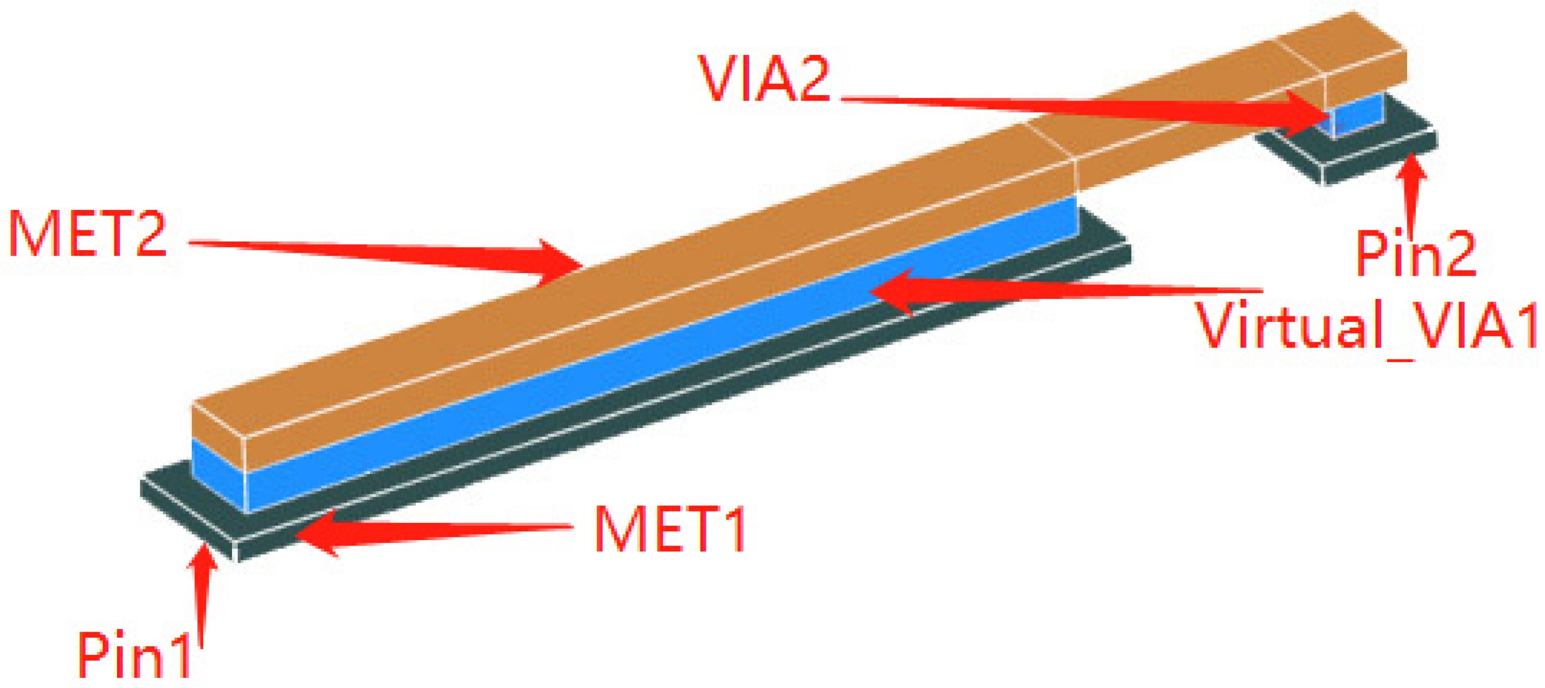
The first example is a flat plate capacitor as shown in
Figure 5. In
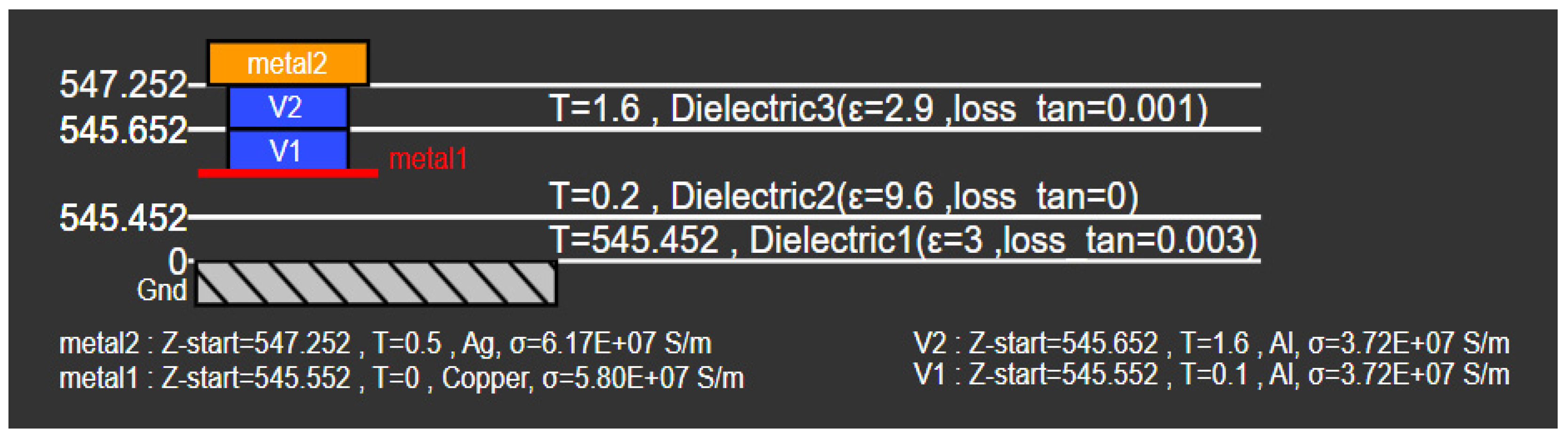
Figure 5, MET1 and MET2 are two metal layers. Virtual_VIA1 is a via layer that connects to MET2 upwards and is apart with a small gap (i.e., 150 nm) from MET1 below. The small gap between Virtual_VIA1 and MET1 forms the main part of the on-chip flat plate capacitor. VIA2 is another via layer that connects MET1 and MET2. The settings and diagram of layers MET1, MET2, Virtual_VIA1 and VIA2 are illustrated in
Figure 6 and
Figure 7, respectively.
Figure 5 is a 3D view of the device under design which needs to be meshed.
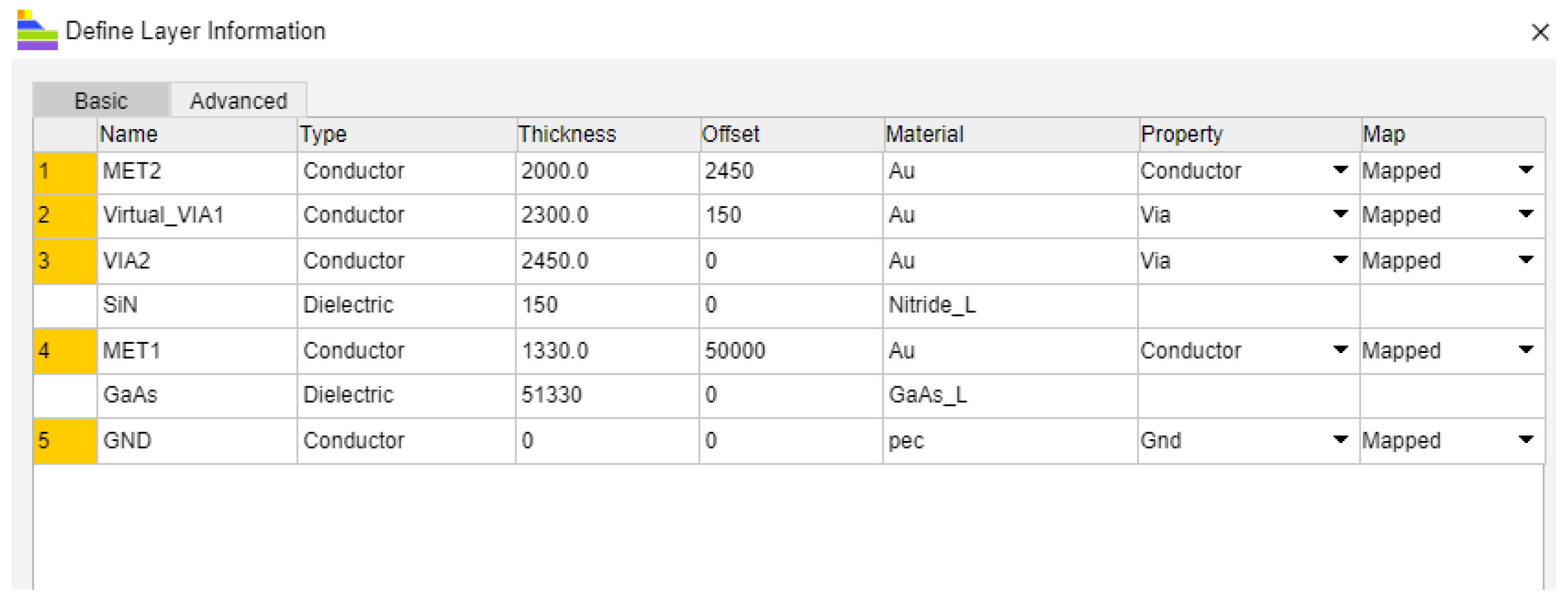
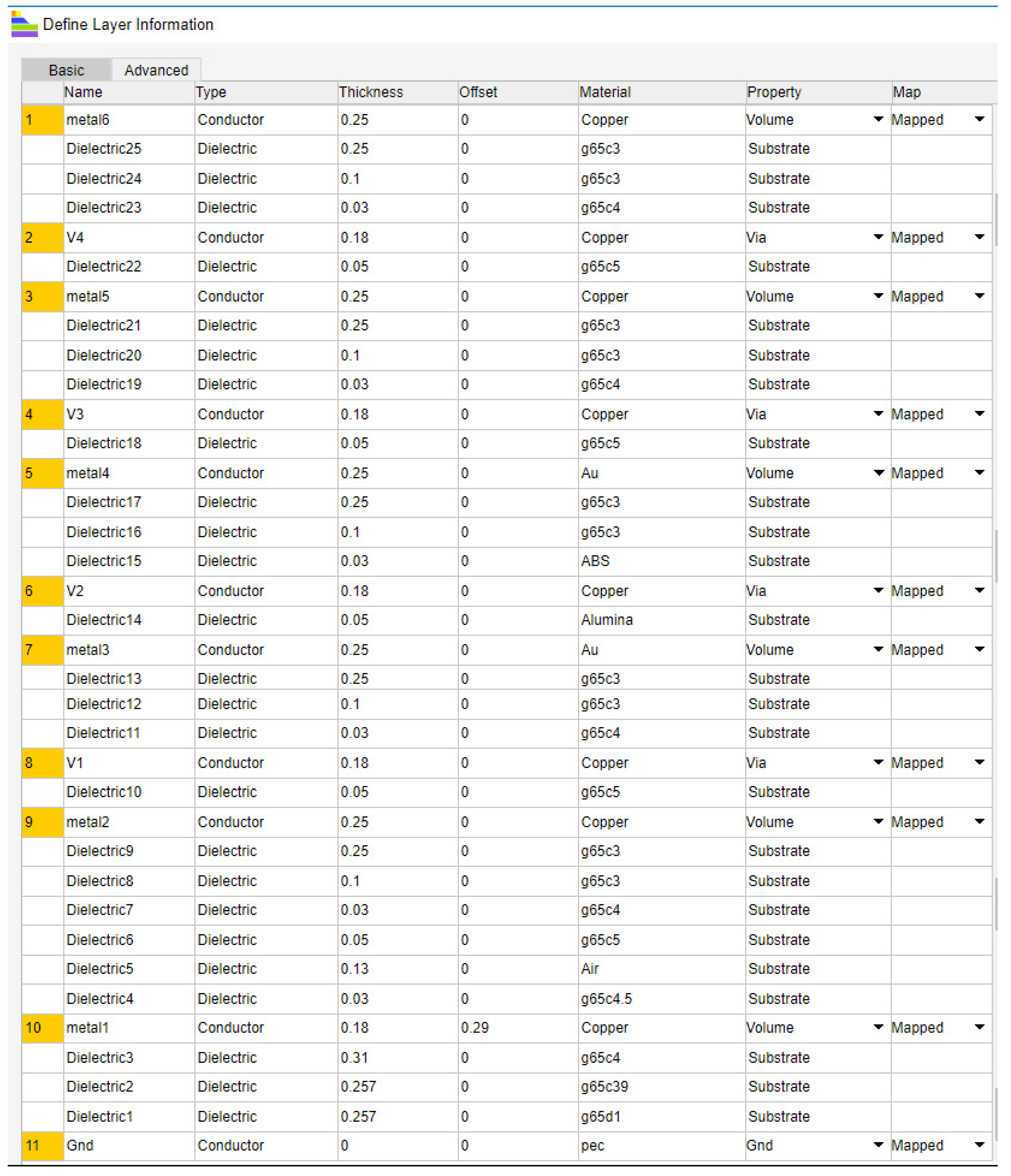
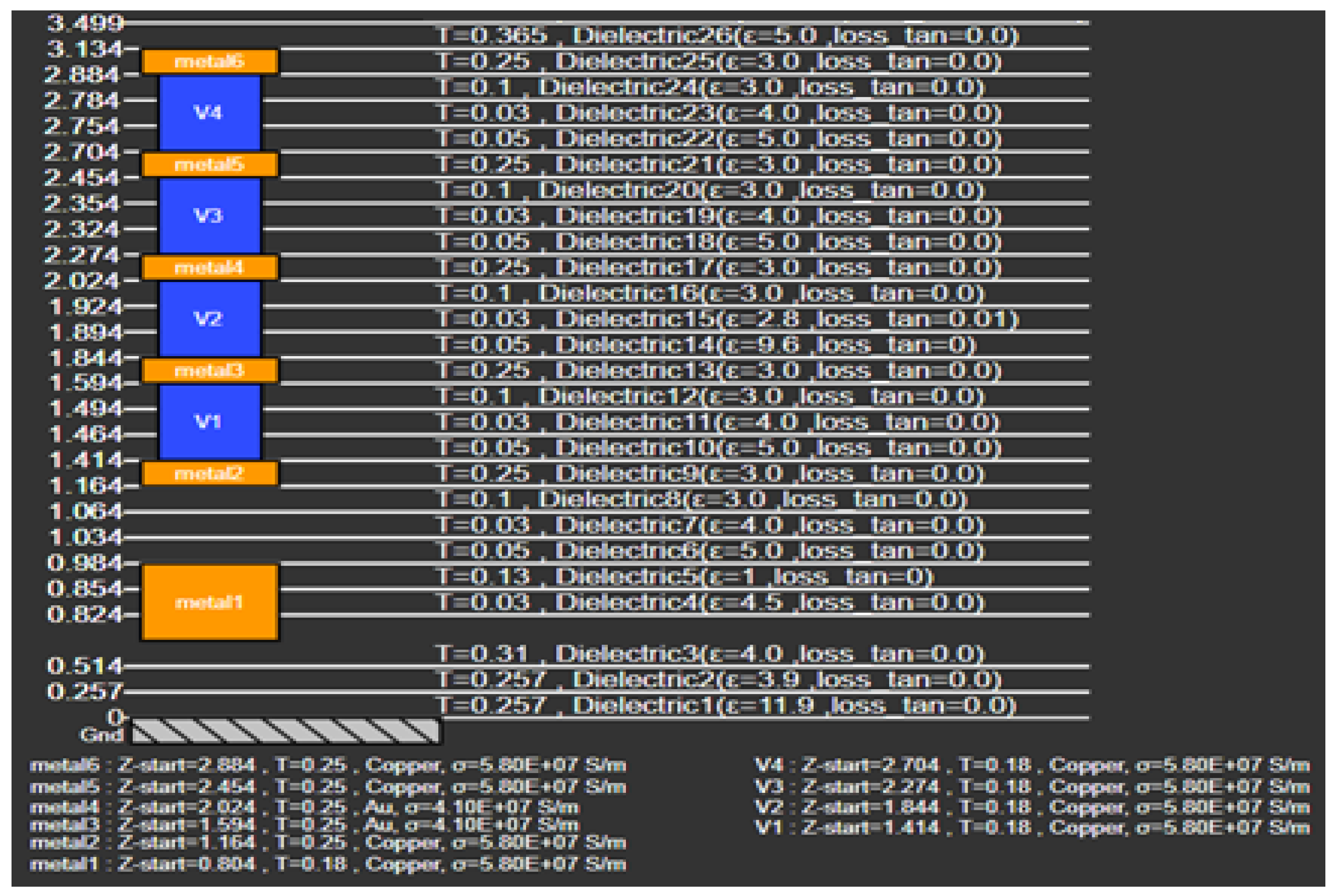
Figure 6 defines the RFIC process data with geometrical and physical properties for all the stack layers, such as the substrate, dielectric stack layers, and metal layers. This figure includes names, thicknesses, and material properties of all the layers. From this figure, it can be seen that there is a 150 nm gap between the VIA2 layer and the Virtual_VIA1 layer.
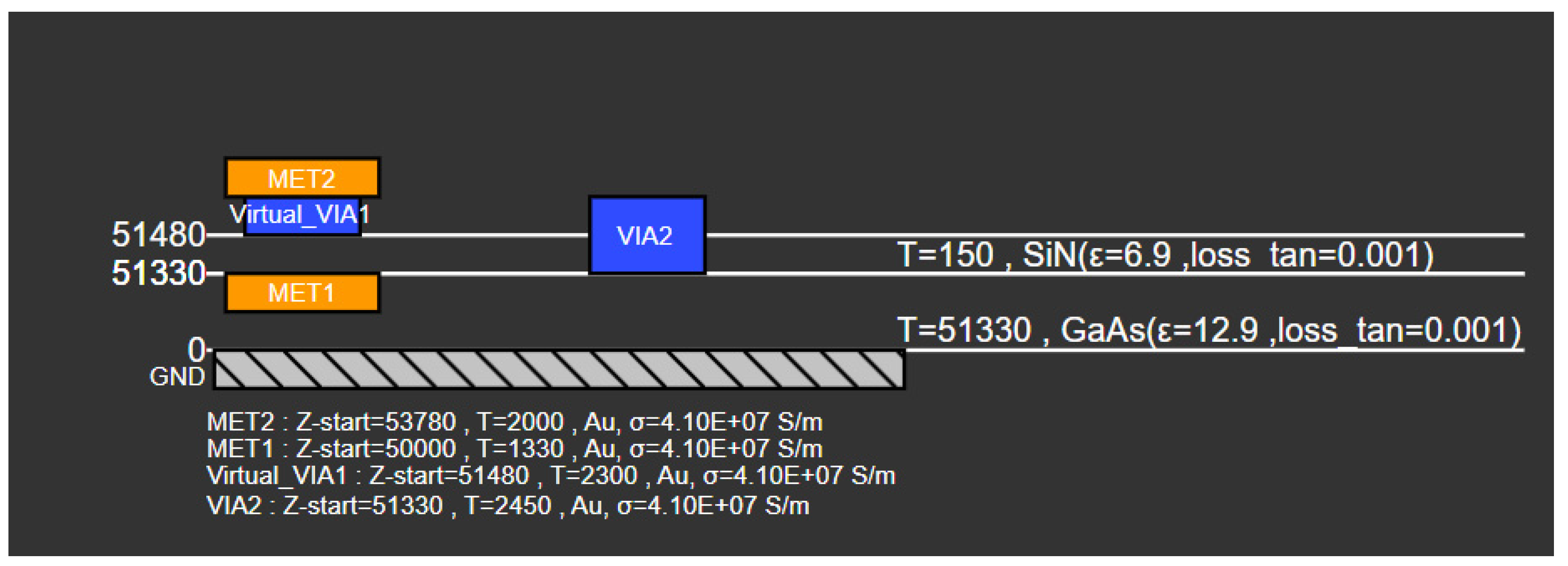
Figure 7 is a visual representation of the table in
Figure 6.
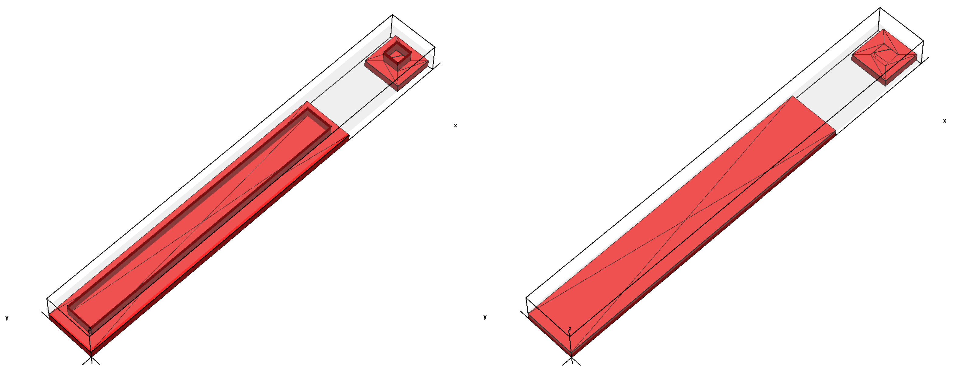
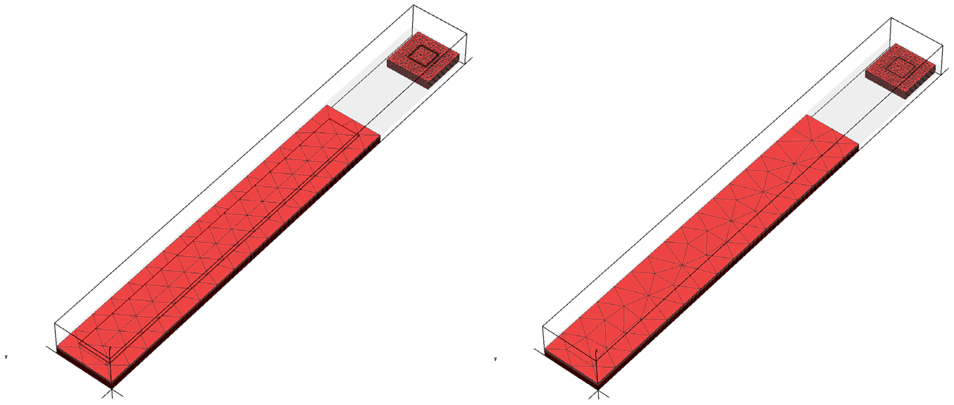
The longest dimension of the entire design is 70 microns, whereas the widest dimension is nine microns. The highest frequency under consideration is 40 GHz. Hence, the device size is very small in comparison with the wavelength of electromagnetic waves under consideration. In general, the mesh size must be smaller than one tenth of the wavelength which is readily met by a standard mesh scheme. The upper and lower surfaces are meshed in terms of triangular grids by the standard mesh scheme which results in 79 elements as shown in
Figure 8. The left panel of
Figure 8 illustrates the meshes on the bottom surface of Virtual_VIA1, whereas the right panel of
Figure 8 shows the meshes on the upper surface of MET1. It can be seen that these two meshes on the bottom surface of Virtual_VIA1 and the upper surface of MET1 are quite different and do not coincide with each other.
It takes 30 s to complete the computation with a memory requirement of 831.18 MB.
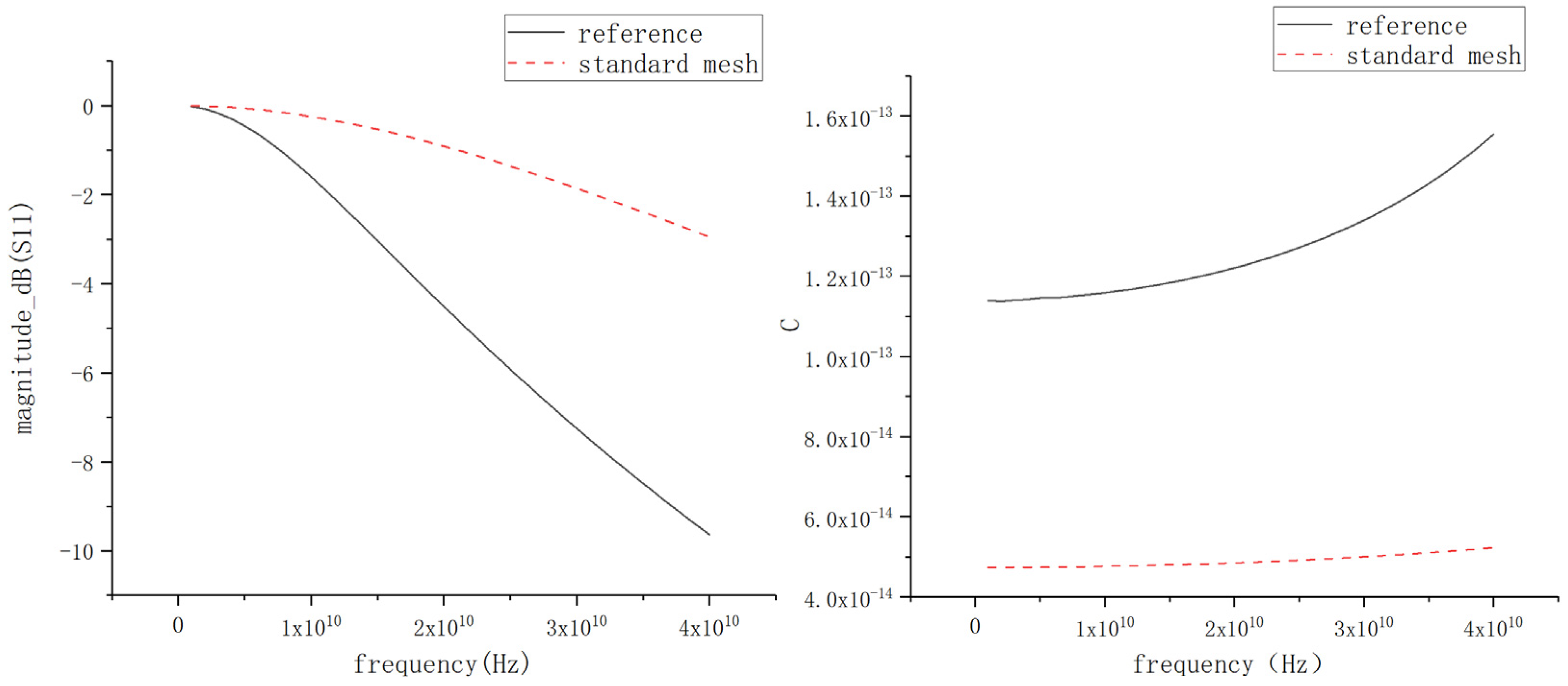
Figure 9 shows the simulation results of the S-parameter (S11) and capacitance using the meshes from
Figure 8 in comparison with the accurate reference results. One can observe that both the S-parameter and capacitance exhibit large errors by comparison with the accurate reference results. Moreover, as the frequency increases, the errors tend to become bigger.
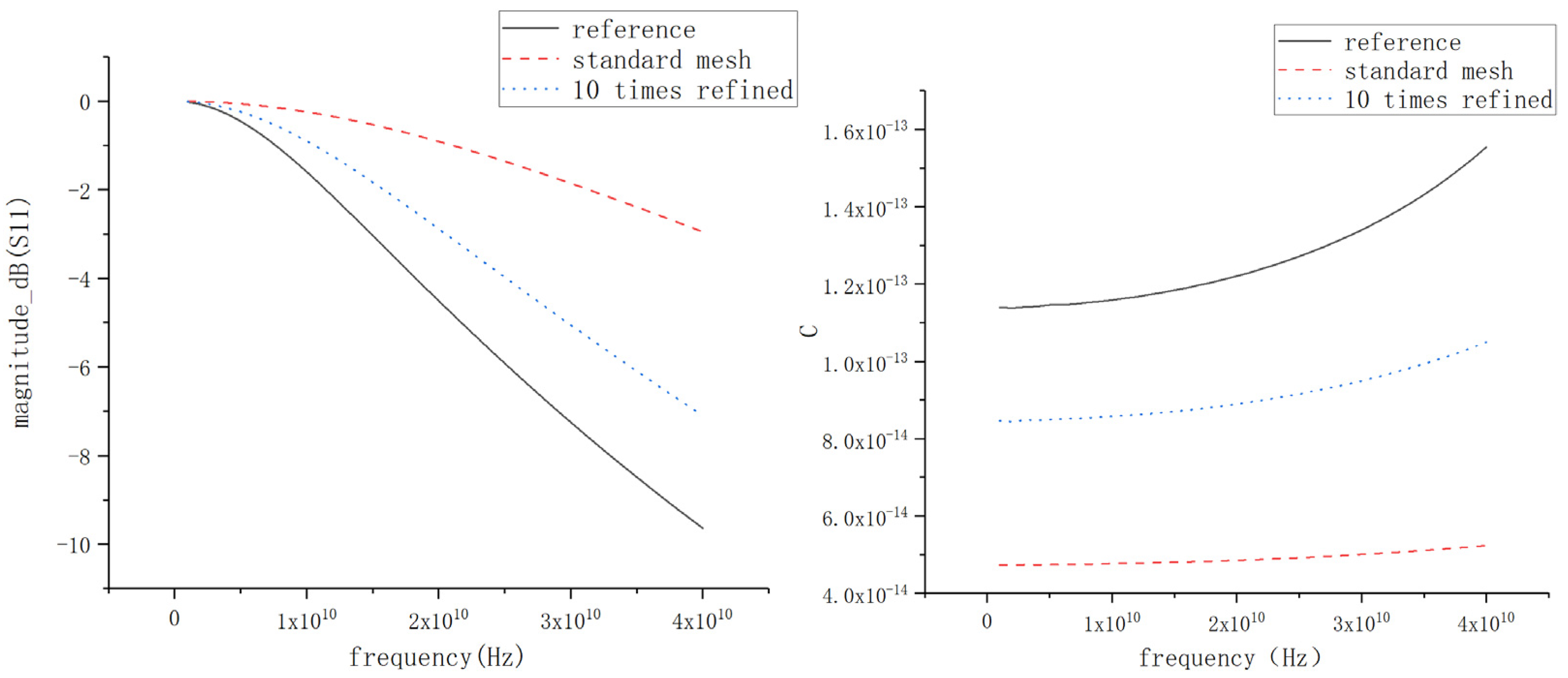
Now, the meshes are refined to be 10 times denser as shown in
Figure 10. The number of elements reaches 1633 at this time. It takes 5.95 min to complete the computation with a memory requirement of 1208.04 MB. The simulation results of the S-parameter (S11) and capacitance using the 10 times refined meshes from
Figure 10 are added as shown in
Figure 11. One can observe that the simulation results with 10 times refined meshes are much closer to the accurate reference results. However, the errors are still quite significant.
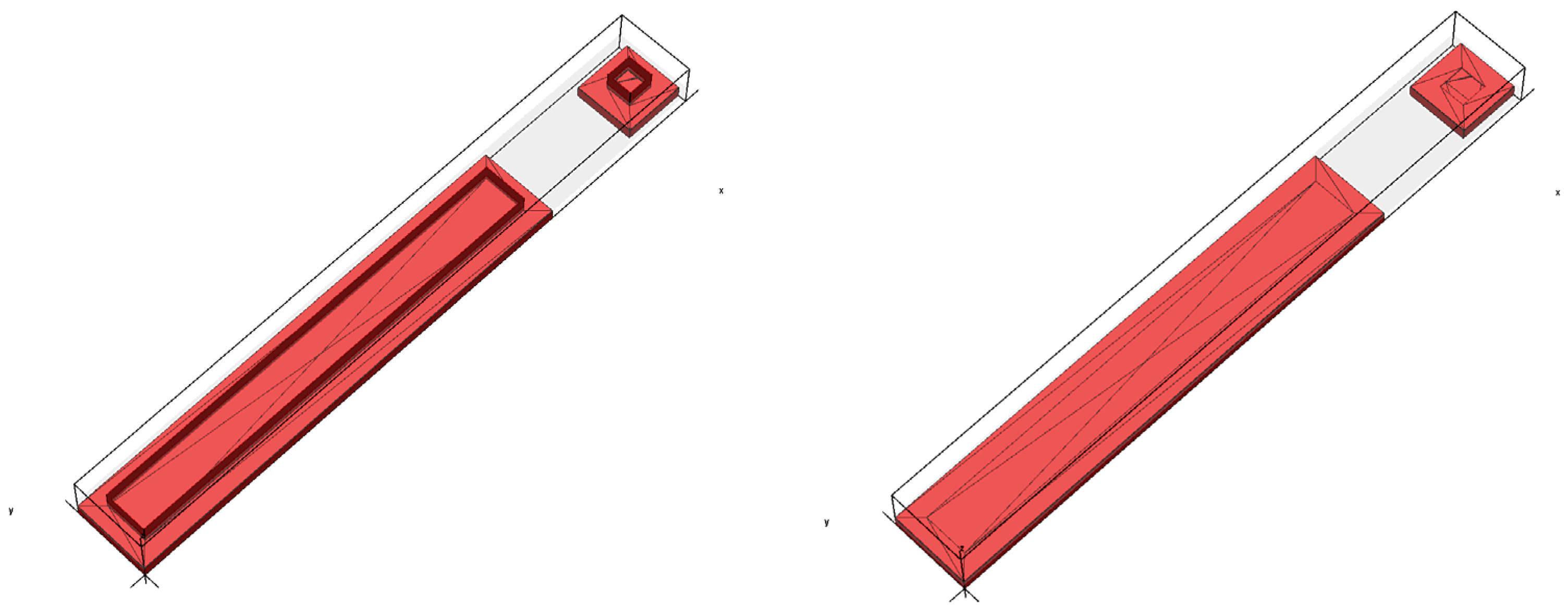
By using the proposed projection mesh scheme, the meshes on the bottom surface of Virtual_VIA1 are directly mapped on the upper surface of MET1 as shown in
Figure 12. The number of elements is only 85. It takes 27.6 s to complete the computation with a memory requirement of 834.29 MB. The simulation results of the S-parameter (S11) and capacitance using the projection mesh scheme are added as shown in
Figure 13. It can be seen that the simulation results from the projection mesh scheme give the closest results to the accurate reference ones. The simulation results, CPU times, and memory consumptions of the above three different mesh schemes are summarized in
Table 1.
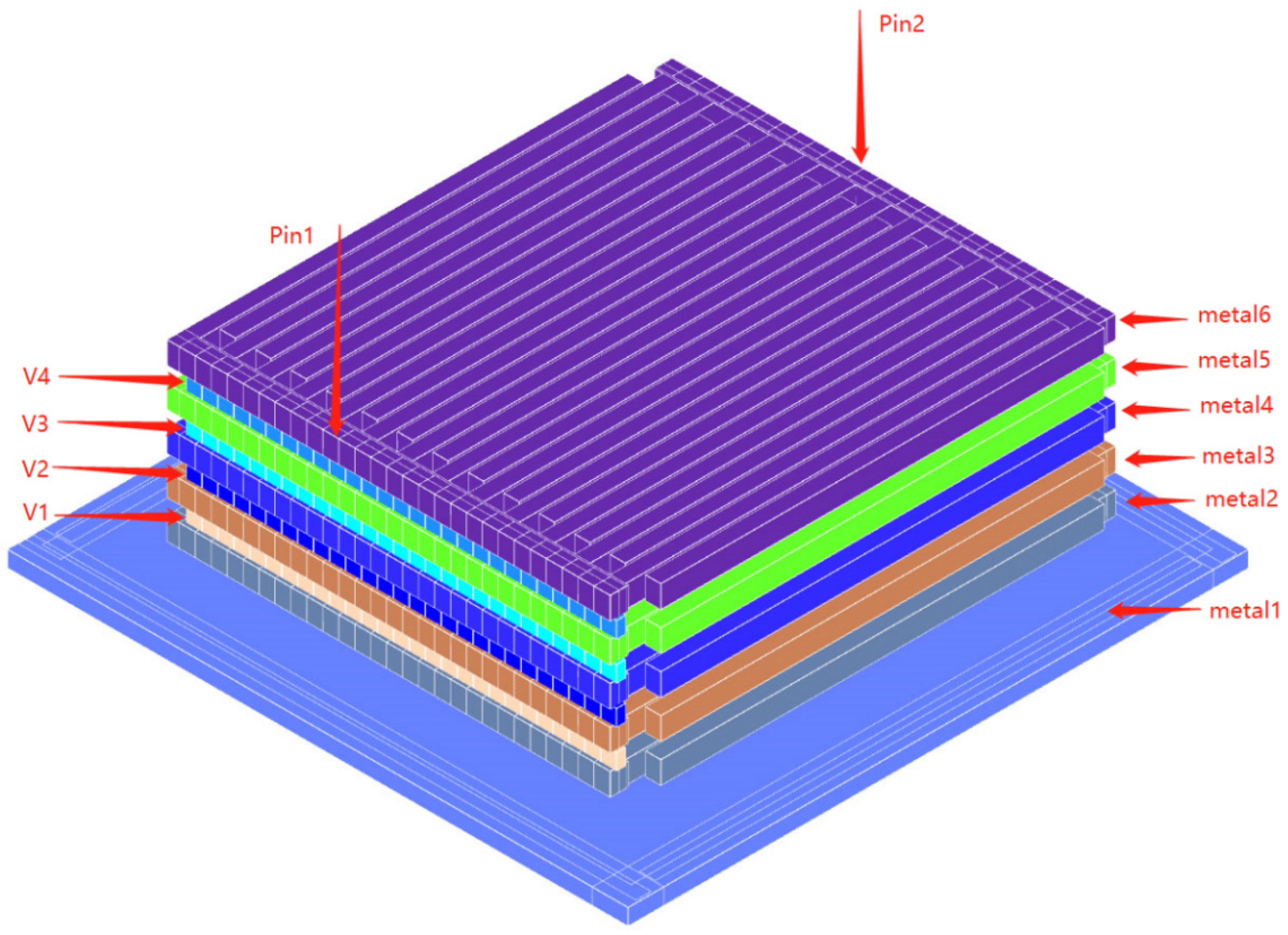
The second example is an on-chip finger capacitor as shown in
Figure 14 which consists of five single-layer finger capacitors on metal layers metal2, metal3, metal4, metal5, and metal6. All the single-layer finger capacitors are combined together to form the on-chip finger capacitor through metal vias on via layers V1, V2, V3, and V4.
Figure 15 and
Figure 16 illustrate the layer settings and diagram, respectively.
Two types of meshes, which are generated by the standard mesh method and the projection scheme, respectively, are examined.
Figure 17 shows the detailed mesh elements generated by the standard mesh method, in which the mesh elements are not well aligned.
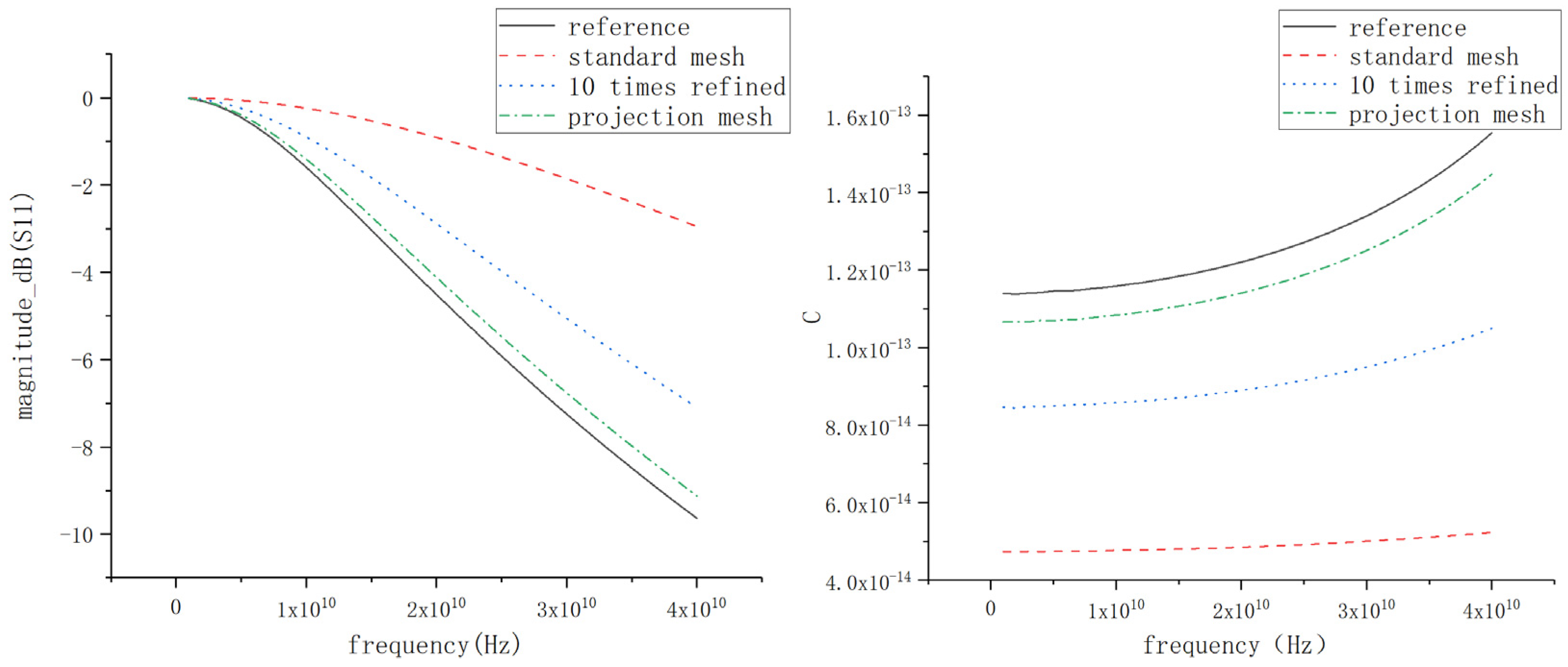
Figure 18 shows the simulation results of the S-parameter (S11) and capacitance using the meshes from
Figure 17 in comparison with the accurate reference results. One can observe that both the S-parameter and capacitance exhibit large errors by comparison with the accurate reference results.
Figure 19 shows the detailed mesh elements generated by the projection scheme, in which the mesh elements on different layers are well aligned. The simulation results of the S-parameter (S11) and capacitance using the projection mesh scheme are added as shown in
Figure 20. It can be seen that the simulation results from the projection mesh scheme give the closest results to the accurate reference ones.
- (e)
Edge refinement
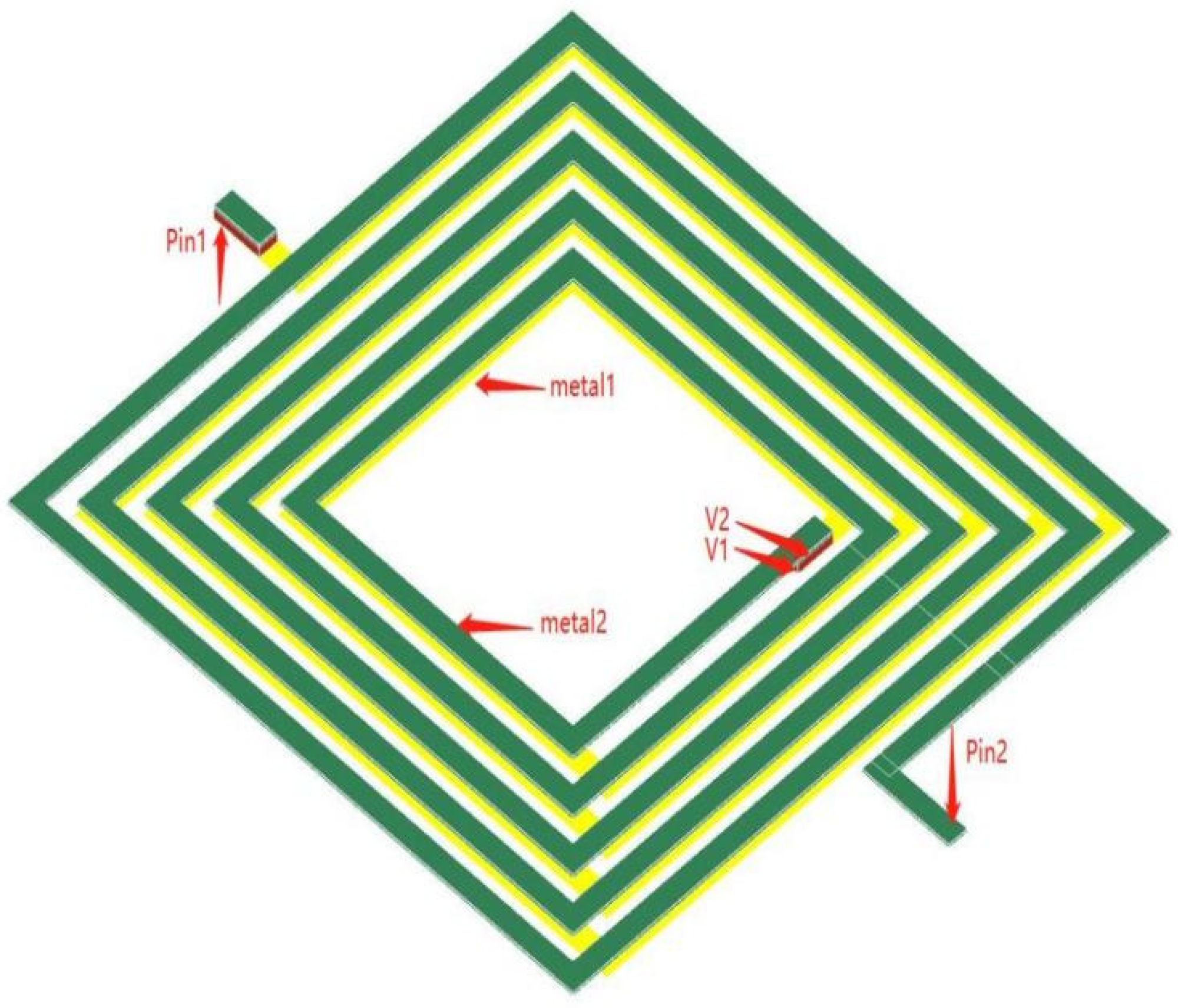
The third example is an on-chip two-layer quadrilateral spiral inductor as shown in
Figure 21. This quadrilateral spiral inductor comprises the rectangular metal structures on layers metal1 and metal2 which are vertically connected by vias on via layers V1 and V2. Two pins are defined on metals (i.e., Pin1) and metal2 (i.e., Pin2).
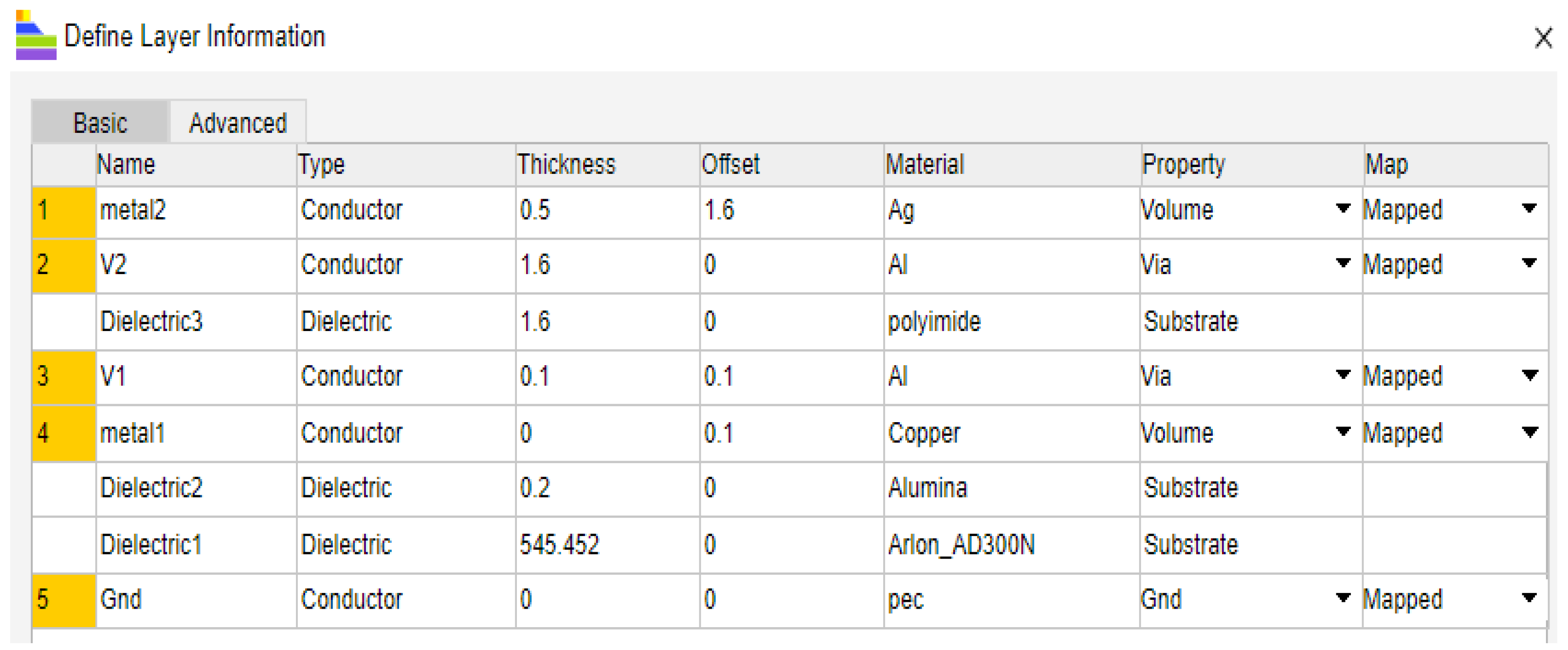
Figure 22 and
Figure 23 illustrate the layer settings and diagram, respectively.
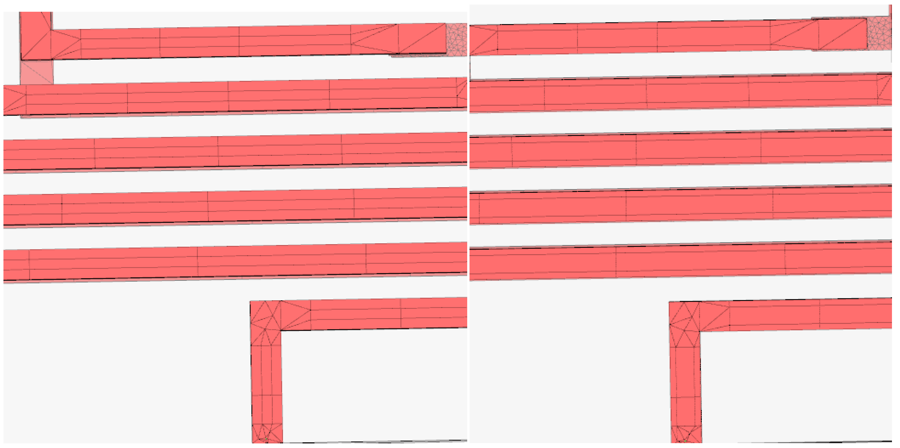
Two types of meshes, which are generated by the standard mesh method and the edge refinement scheme, respectively, are examined.
Figure 24 compares the meshes generated by the standard mesh method (i.e., the left panel) and the edge refinement scheme (i.e., the right panel). The mesh elements from the edge refinement scheme are finer at the edges than those in the middle of metal traces.
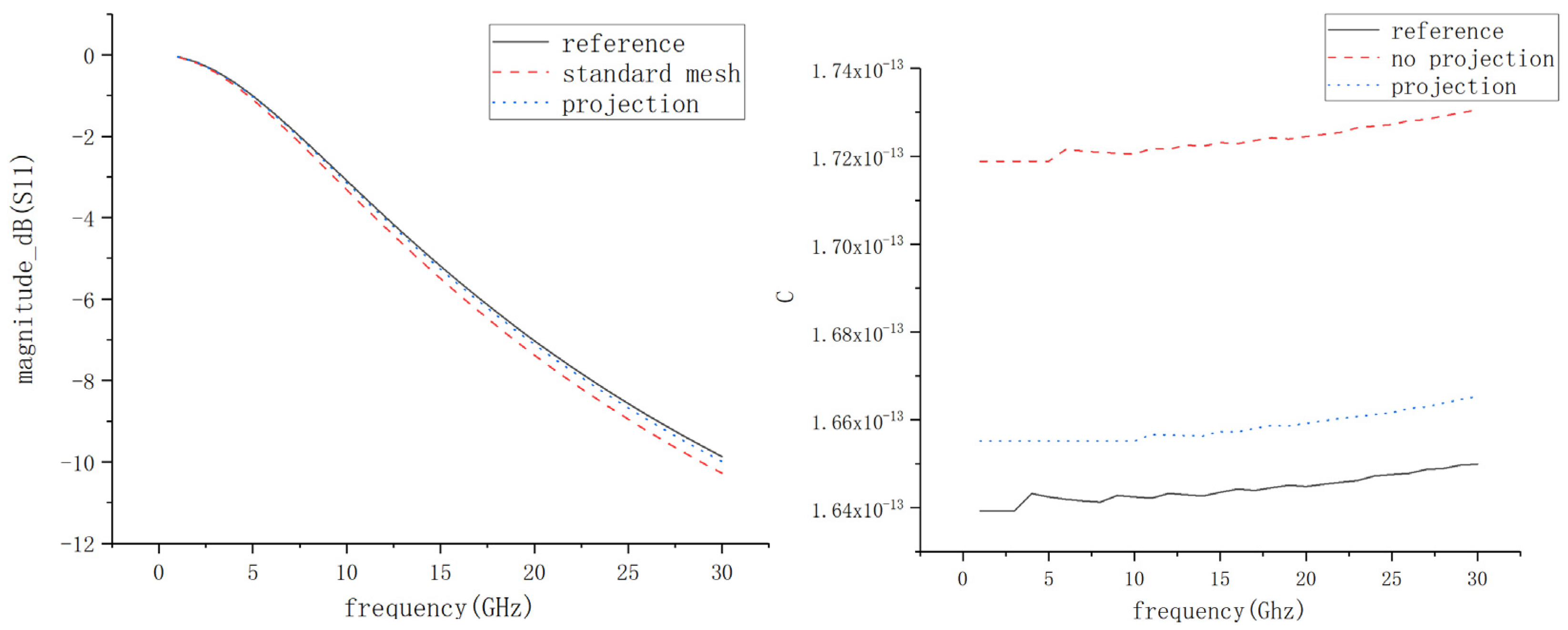
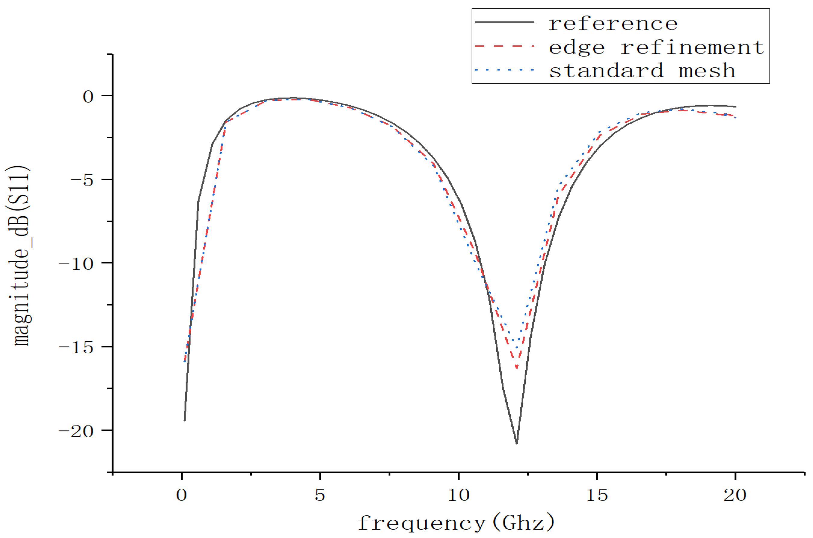
Figure 25 shows the simulation results of the S-parameter (S11) for both the meshes from
Figure 24 in comparison with the accurate reference results. It can be observed that the S-parameter result with edge refinement is more accurate than that without edge refinement.
- (f)
Via aggregation
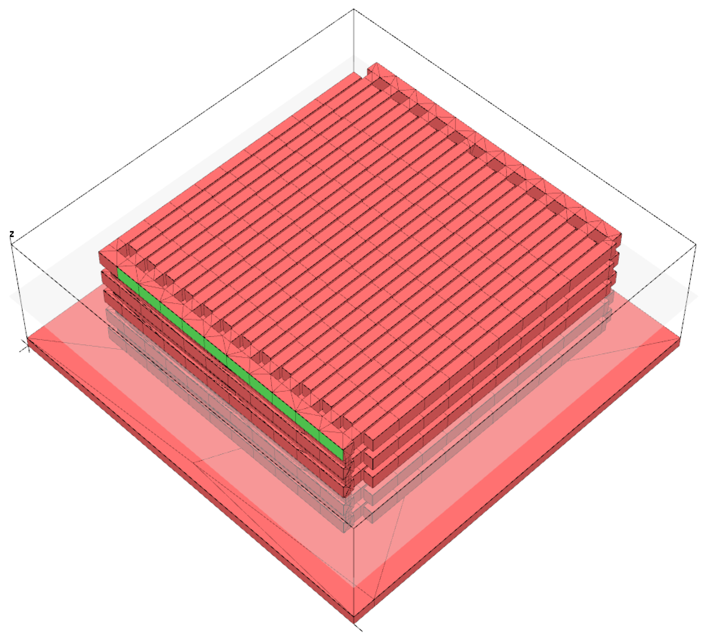
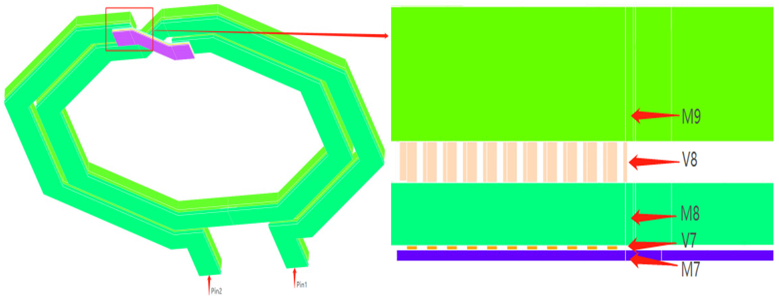
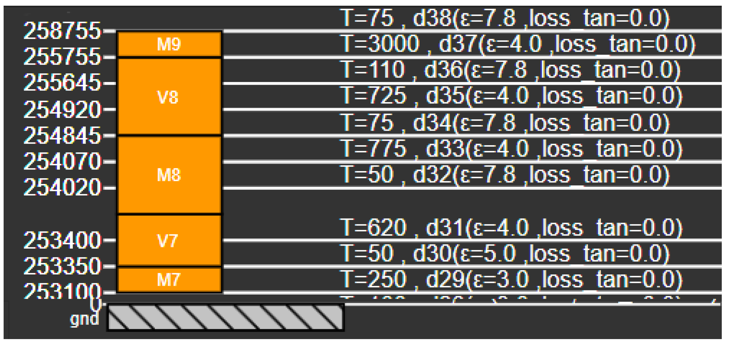
The final example is an on-chip multi-layer octagonal spiral inductor as shown in
Figure 26. The on-chip spiral inductor mainly consists of metal structures on two metal layers M8 and M9 which are vertically connected through a via array on via layer V8. Layers M7 and V7 are used to form the bridge at the two ends of the crossover winding on M8. From the perspective view on the right panel of
Figure 26, it can be seen that V7 and V8 are the via layers used for vertical connections of the metal layers and the metal structures on these layers are all via arrays.
Figure 27 and
Figure 28 illustrate the layer settings and diagram, respectively.
Due to the large number of vias in the via array, the electromagnetic computation consumes a significant amount of CPU time and memory resource. For example, by using the brute-force standard mesh method, the entire electromagnetic computation could consume 23,311 min of CPU time, and 117,908 MB of memory resource.
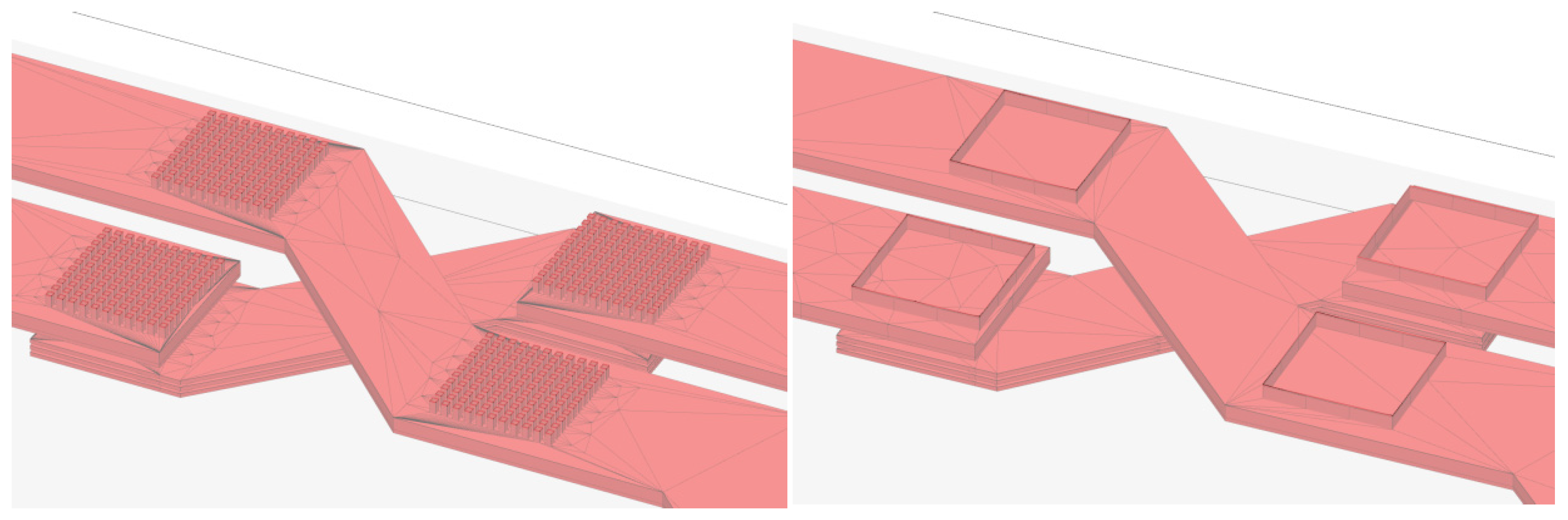
To circumvent this difficulty, the proposed via aggregation method can be employed to improve computational efficiency without compromising computational accuracy.
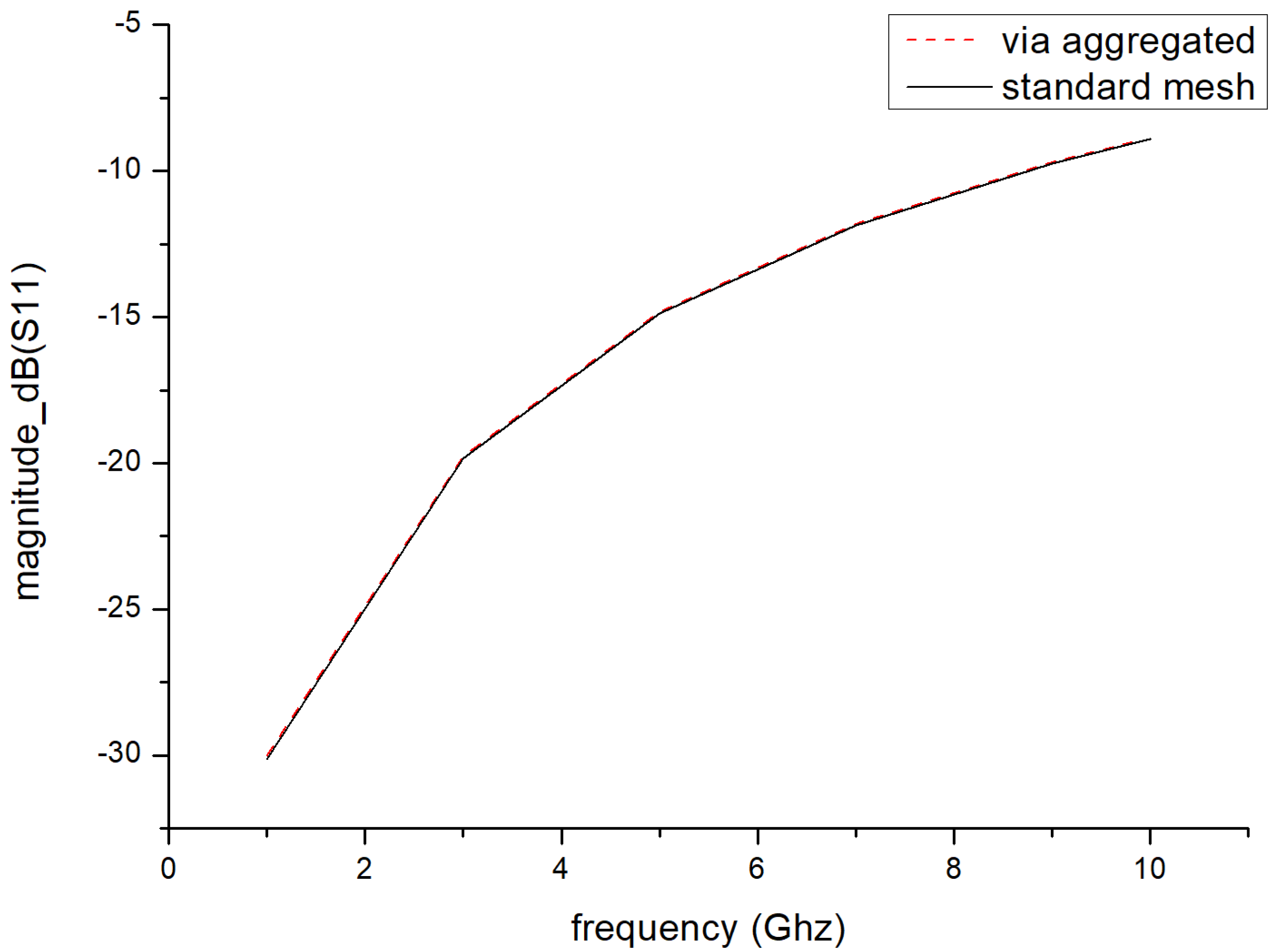
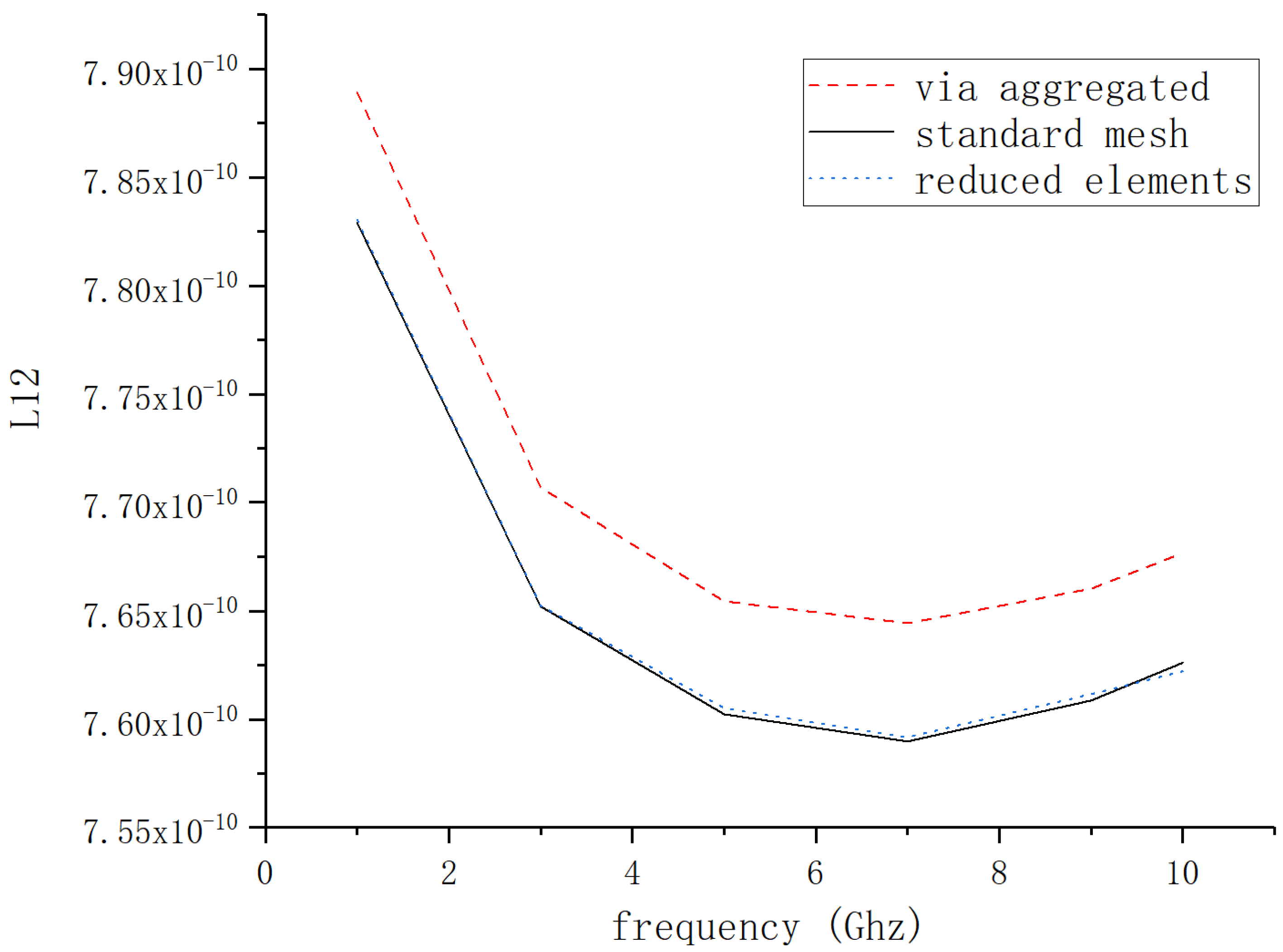
Figure 29 shows the original meshes (i.e., the left panel) from the brute-force standard mesh method and the enhanced meshes (i.e., the right panel) from the via aggregation method on layer V8. The numerical results from both meshes are almost identical as shown in
Figure 30 and
Figure 31. However, the entire electromagnetic computation now only consumes 56 min of CPU time and 3661 MB of memory resources as summarized in
Table 2. As the frequency increases, the deviation of the via aggregation results enlarges. In the frequency range under consideration, the deviation is acceptable. However, for much higher frequencies, the deviation may become unacceptable, in which the original massive vias without aggregation need to be used and force-brutely treated.
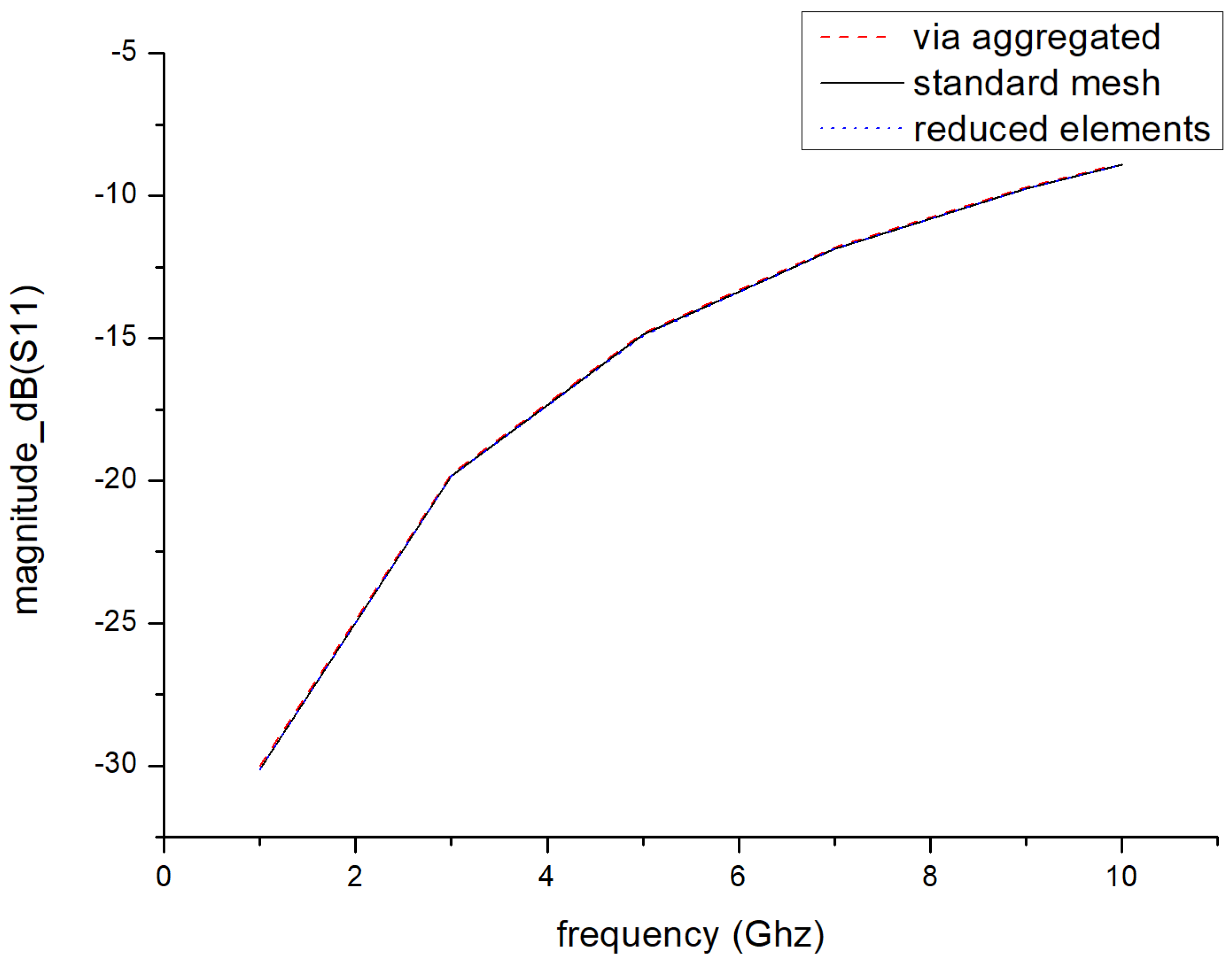
The results obtained by reducing the number of elements on vias are presented in
Figure 32 and
Figure 33. Although the results are closer to the original results, the computational cost is still in the same order of magnitude as that of the original standard mesh method.


