A 237 GHz Traveling Wave Tube for Cloud Radar


Abstract
:1. Introduction
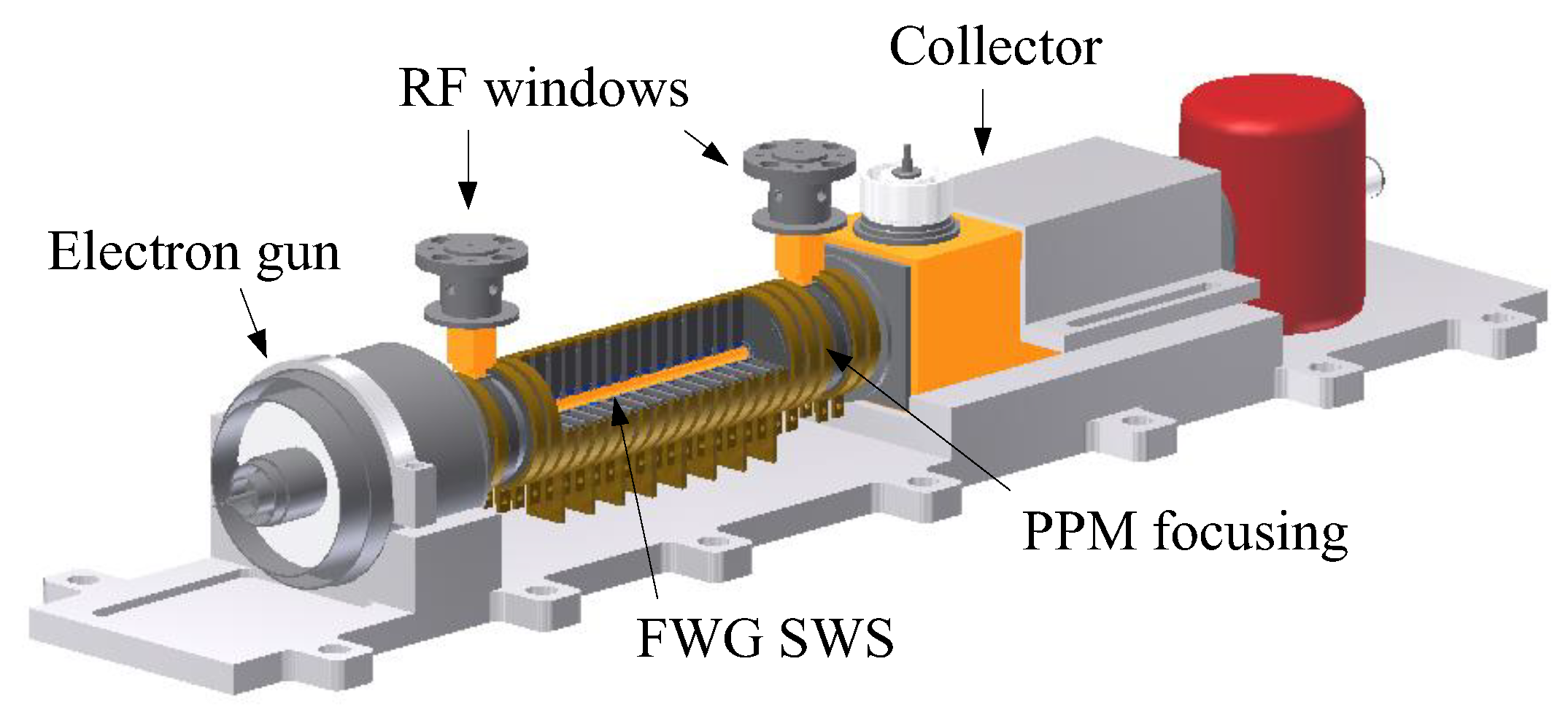
2. Systems Design
- a.
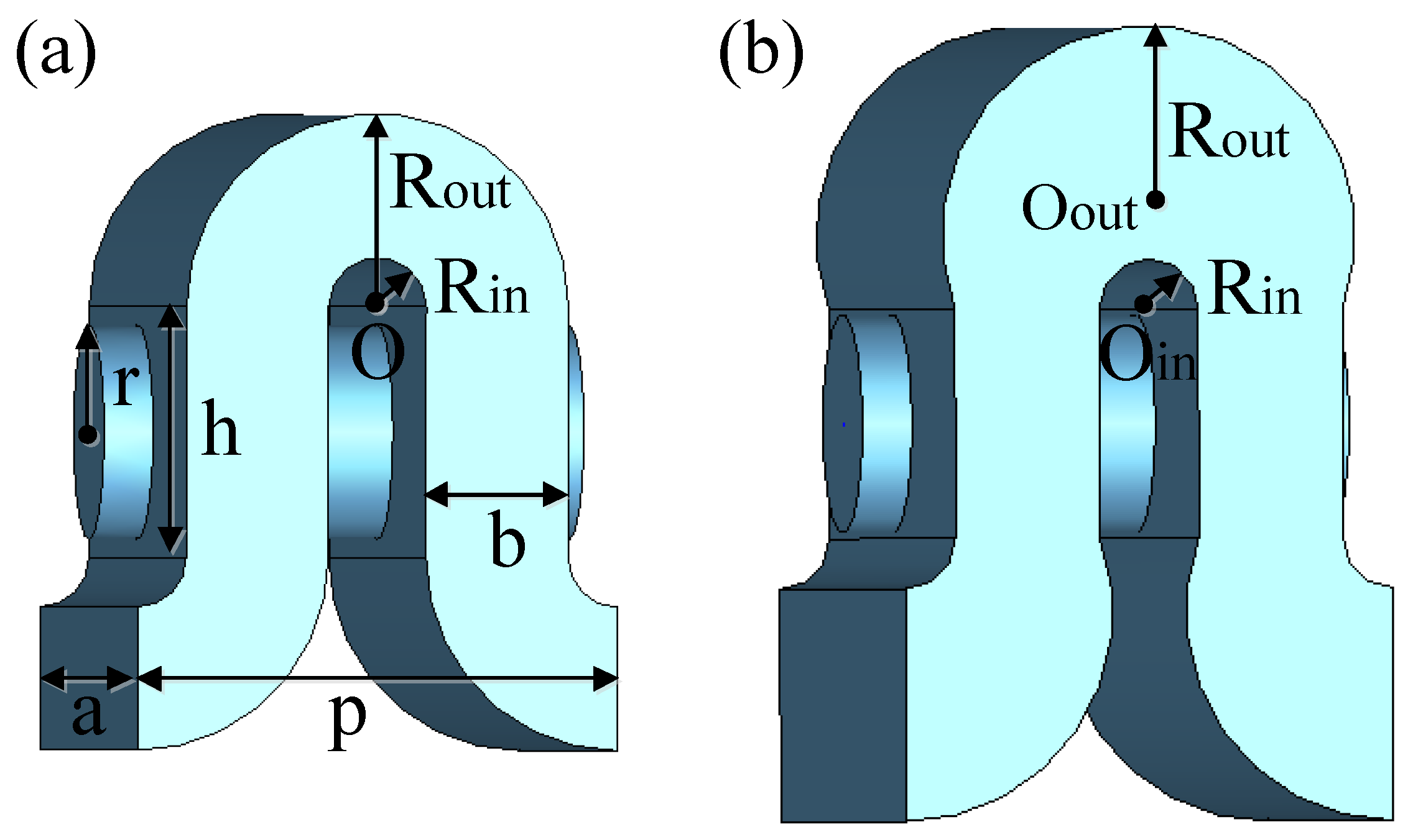
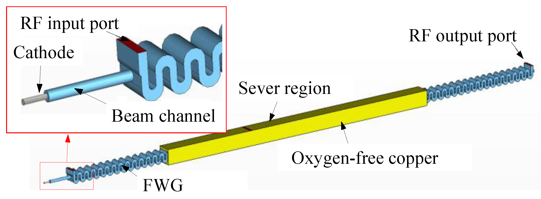
- SWS Design
- b.
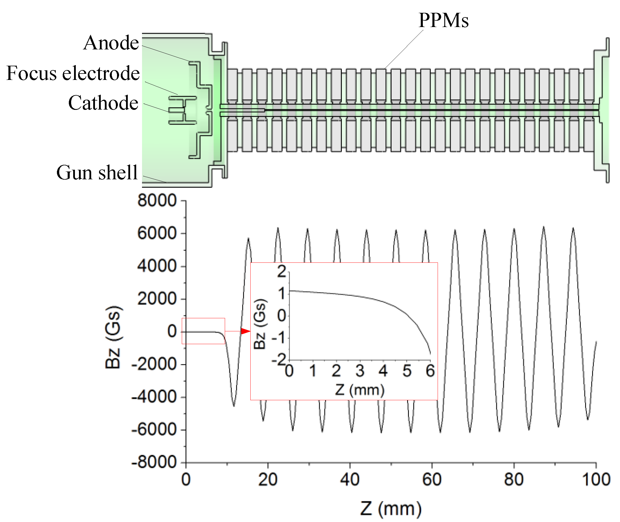
- Electron Optical System
- c.
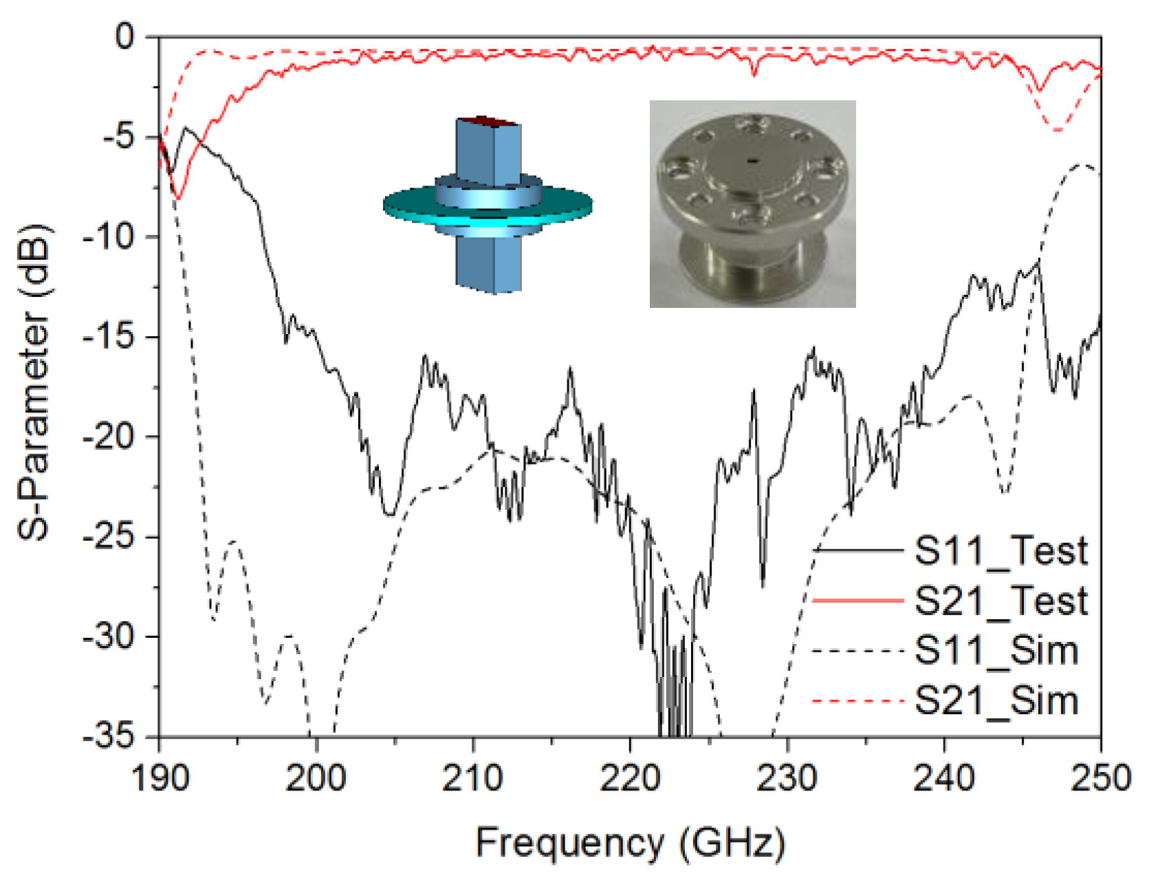
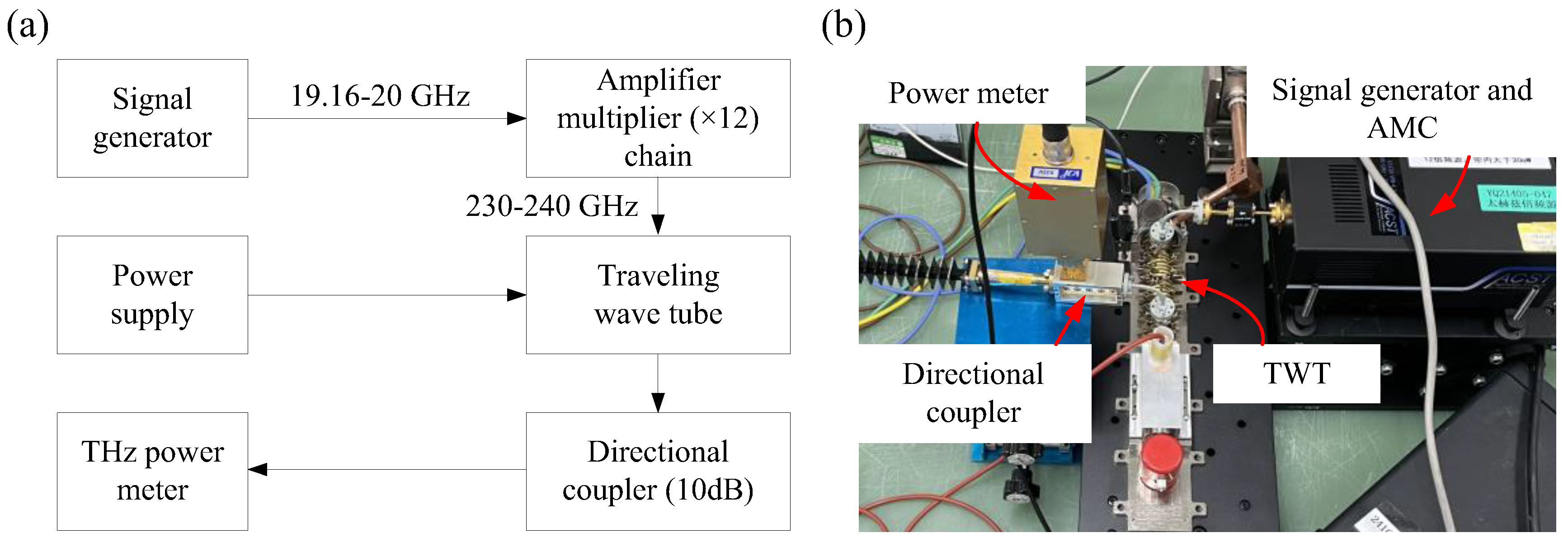
- Energy Transmission System
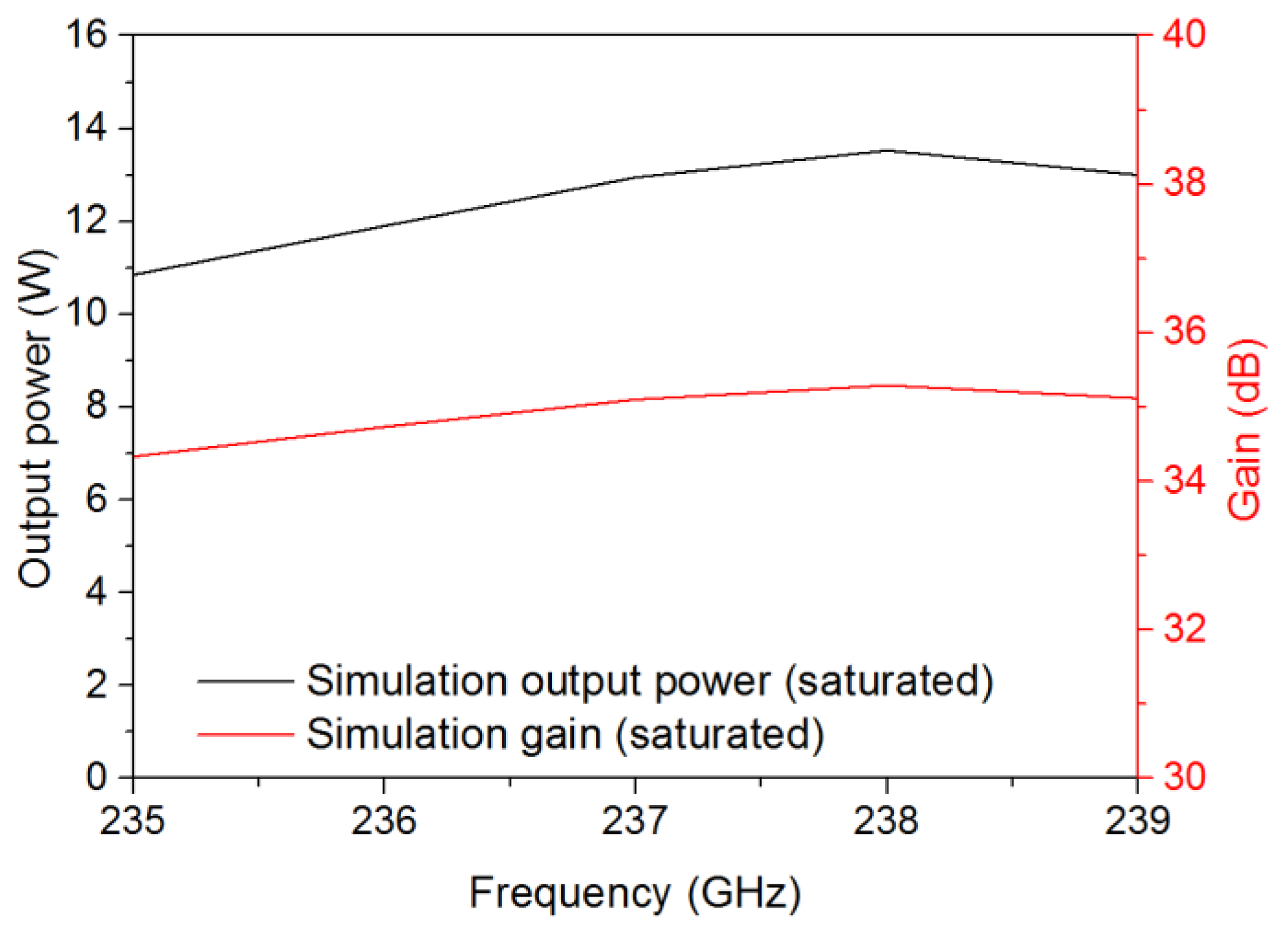
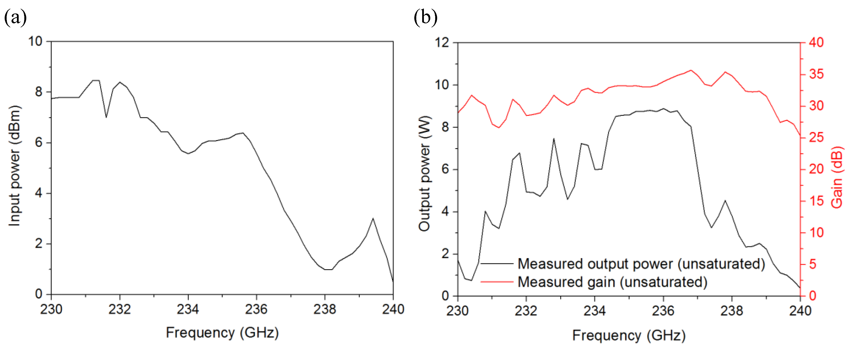
3. TWT Performance
4. Conclusions
Author Contributions
Funding
Data Availability Statement
Conflicts of Interest
References
- Sassen, K.; Wang, Z. Classifying clouds around the globe with the CloudSat. Geophys. Res. Lett. 2008, 35, L04805. [Google Scholar] [CrossRef]
- Walker McLinden, M.L.; Li, L.; Heymsfield, G.M.; Coon, M.; Emory, A. The NASA GSFC 94-GHz Airborne Solid-State Cloud Radar System (CRS). J. Atmos. Ocean. Technol. 2021, 38, 1001–1017. [Google Scholar] [CrossRef]
- Battaglia, A.; Kollias, P.; Dhillon, R.; Roy, R.; Tanelli, S.; Lamer, K.; Grecu, M.; Lebsock, M.; Watters, D.; Mroz, K.; et al. Spaceborne Cloud and Precipitation Radars: Status, Challenges, and Ways Forward. Rev. Geophys. Adv. Earth Space Sci. 2020, 58, e2019RG000686. [Google Scholar] [CrossRef] [PubMed]
- McIntosh, R.; Narayanan, R.; Mead, J.; Schaubert, D. Design and performance of a 215 GHz pulsed radar system. IEEE Trans. Microw. Theory Tech. 1988, 36, 994–1001. [Google Scholar] [CrossRef]
- Hyttinen, M.; Roitman, A.; Horoyski, P.; Deng, H. High Power Pulsed 263 GHz Extended Interaction Amplifier. In Proceedings of the 2020 IEEE 21st International Conference on Vacuum Electronics (IVEC), Monterey, CA, USA, 19–22 October 2020; pp. 1–2. [Google Scholar] [CrossRef]
- Armstrong, C.M. The truth about terahertz. IEEE Spectr. 2012, 49, 36–41. [Google Scholar] [CrossRef]
- Mendel, J.T.; Quate, C.F.; Yocom, W.H. Electron beam focusing with periodic permanent magnet fields. Proc. IRE 1954, 42, 800–810. [Google Scholar] [CrossRef]
- Sherwin, M. Terahertz power. Nature 2002, 420, 131–133. [Google Scholar] [CrossRef] [PubMed]
- Booske, J.H.; Dobbs, R.J.; Joye, C.D.; Kory, C.L.; Neil, G.R.; Park, G.-S.; Park, J.; Temkin, R.J. Vacuum Electronic High Power Terahertz Sources. IEEE Trans. Terahertz Sci. Technol. 2011, 1, 54–75. [Google Scholar] [CrossRef]
- Basten, M.; Tucek, J.; Gallagher, D.; Kreischer, K. 233 GHz high power amplifier development at Northrop Grumman. In Proceedings of the 2016 IEEE International Vacuum Electronics Conference (IVEC), Monterey, CA, USA, 19–21 April 2016; pp. 1–2. [Google Scholar] [CrossRef]
- Joye, C.D.; Kimura, T.; Hyttinen, M.; Levush, B.; Cook, A.M.; Calame, J.P.; Abe, D.K.; Vlasov, A.N.; Chernyavskiy, I.A.; Nguyen, K.T.; et al. Demonstration of a high power, wideband 220-GHz traveling wave amplifier fabricated by UV-LIGA. IEEE Trans. Electron Devices 2014, 61, 1672–1678. [Google Scholar] [CrossRef]
- Armstrong, C.M.; Kowalczyk, R.; Zubyk, A.; Berg, K.; Meadows, C.; Chan, D.; Schoemehl, T.; Duggal, R.; Hinch, N.; True, R.B.; et al. A Compact Extremely High Frequency MPM Power Amplifier. IEEE Trans. Electron Devices 2018, 65, 2183–2188. [Google Scholar] [CrossRef]
- Bian, X.; Pan, P.; Tang, Y.; Lu, Q.; Li, Y.; Zhang, L.; Wu, X.; Cai, J.; Feng, J. Demonstration of a Pulsed G-Band 50-W Traveling Wave Tube. IEEE Electron Device Lett. 2020, 42, 248–251. [Google Scholar] [CrossRef]
- Pan, P.; Tang, Y.; Bian, X.; Zhang, L.; Lu, Q.; Li, Y.; Feng, Y.; Feng, J. A G-Band Traveling Wave Tube with 20 W Continuous Wave Output Power. IEEE Electron Device Lett. 2020, 41, 1833–1836. [Google Scholar] [CrossRef]
- YFeng, Y.; Bian, X.; Song, B.; Li, Y.; Pan, P.; Feng, J. A G-Band Broadband Continuous Wave Traveling Wave Tube for Wireless Communications. Micromachines 2022, 13, 1635. [Google Scholar] [CrossRef]
- Hu, P.; Lei, W.; Jiang, Y.; Huang, Y.; Song, R.; Chen, H.; Dong, Y. Demonstration of a Watt-Level Traveling Wave Tube Amplifier Operating Above 0.3 THz. IEEE Electron Device Lett. 2019, 40, 973–976. [Google Scholar] [CrossRef]
- Cai, J.; Feng, J.; Wu, X. Folded Waveguide Slow Wave Structure with Modified Circular Bends. IEEE Trans. Electron Devices 2014, 61, 3534–3538. [Google Scholar] [CrossRef]
- CST Particle Studio. CST Computer Simulation Technology GmBH. [Online]. Available online: http://www.cst.com (accessed on 10 March 2020).
- Pan, P.; Li, H.; Feng, J. Study on loss of folded waveguide structures of 220 GHz and 340 GHz. In Proceedings of the 2016 IEEE International Vacuum Electronics Conference (IVEC), Monterey, CA, USA, 19–21 April 2016; pp. 1–2. [Google Scholar] [CrossRef]
- Gilmour, J.A.S. Klystrons, Traveling Wave Tubes, Magnetrons, Crossed-Filed Ampliers, and Gyrotrons; Artech House: Norfolk County, MA, USA, 2011. [Google Scholar]
- Zienkiewicz, O.C.; Taylor, R.L.; Zhu, J.Z. The Finite Element Method: Its Basis and Fundamentals; Elsevier: Amsterdam, The Netherlands, 2005. [Google Scholar]
- Ding, M.Q.; Li, L.; Feng, J. A study of high-quality freestanding diamond films grown by MPCVD. Appl. Surf. Sci. 2012, 258, 5987–5991. [Google Scholar] [CrossRef]


| Symbol | Geometric Parameters | Normal FWG SWS | FWG SWS with Modified Circular Bends |
|---|---|---|---|
| p (µm) | Period Length | 532 | 540 |
| b (µm) | Height of Waveguide | 160 | 160 |
| a (µm) | Width of Waveguide | 760 | 760 |
| h (µm) | Length of Waveguide | 240 | 240 |
| r (µm) | Beam Channel Radius | 120 | 120 |
| Rout (µm) | Outer Radius | 213 | 300 |
| Rin (µm) | Inner Radius | 55 | 55 |
| Oout − Oin (µm) | Distance of the Arc Center | 0 | 30 |
Disclaimer/Publisher’s Note: The statements, opinions and data contained in all publications are solely those of the individual author(s) and contributor(s) and not of MDPI and/or the editor(s). MDPI and/or the editor(s) disclaim responsibility for any injury to people or property resulting from any ideas, methods, instructions or products referred to in the content. |
© 2023 by the authors. Licensee MDPI, Basel, Switzerland. This article is an open access article distributed under the terms and conditions of the Creative Commons Attribution (CC BY) license (https://creativecommons.org/licenses/by/4.0/).
Share and Cite
Li, Y.; Pan, P.; Song, B.; Zhang, L.; Feng, J. A 237 GHz Traveling Wave Tube for Cloud Radar. Electronics 2023, 12, 2153. https://doi.org/10.3390/electronics12102153
Li Y, Pan P, Song B, Zhang L, Feng J. A 237 GHz Traveling Wave Tube for Cloud Radar. Electronics. 2023; 12(10):2153. https://doi.org/10.3390/electronics12102153
Chicago/Turabian StyleLi, Ying, Pan Pan, Bowen Song, Lin Zhang, and Jinjun Feng. 2023. "A 237 GHz Traveling Wave Tube for Cloud Radar" Electronics 12, no. 10: 2153. https://doi.org/10.3390/electronics12102153
APA StyleLi, Y., Pan, P., Song, B., Zhang, L., & Feng, J. (2023). A 237 GHz Traveling Wave Tube for Cloud Radar. Electronics, 12(10), 2153. https://doi.org/10.3390/electronics12102153