Article

A Single-Stage Bimodal Transformerless Inverter with Common-Ground and Buck-Boost Features

1
Department of Electrical Engineering, Chonnam National University, Gwangju 61186, Republic of Korea
2
Faculty of Electrical and Electronics Engineering, Ho Chi Minh City University of Technology and Education, Ho Chi Minh City 700000, Vietnam
*
Authors to whom correspondence should be addressed.
Electronics 2023, 12(1), 221; https://doi.org/10.3390/electronics12010221
Submission received: 16 December 2022 / Revised: 29 December 2022 / Accepted: 30 December 2022 / Published: 2 January 2023
(This article belongs to the Special Issue Single-Stage DC-AC Power Conversion Systems)

Abstract

:
This paper proposes a single-phase, single-stage common-ground inverter with a non-electrolytic capacitor and buck-boost ability. The proposed single-stage inverter is employed by a boost stage DC-DC converter and bimodal circuit, which makes it satisfactory for PV systems with a wide input voltage range and lower switch voltage stress. The leakage current of the proposed single-stage inverter can effectively suppress because the parasitic capacitor between the PV panel and the ground is shortened. In addition, the proposed single-stage inverter does not include electrolytic capacitors, which reduces the equivalent series resistance of electrolytic capacitors and also the size of the inverter system. The topology, operating principle, and PWM control method of the proposed single-stage inverter are given. The design guidelines of components and comparative studies of the proposed single-stage inverter are provided. A 500 W laboratory prototype of the proposed single-stage inverter is built to verify the correctness of the simulation and theoretical analysis.

1. Introduction

Nowadays, the issue of energy is becoming a major concern for the speedy development of human society. The over-exploitation of traditional energy sources causes many environmental problems, which significantly affect the development of society. Therefore, a stable and environmentally friendly energy needs to be researched and developed. Renewable energy sources have been widely used in the world; among them, solar energy has many advantages in terms of reserves, environmental protection, and ease of development [1,2,3,4,5]. As a fundamental component of solar energy production, photovoltaic (PV) inverter has attracted the interest of many scholars. According to the structure of the inverter, PV inverters can be divided into isolated and non-isolated types. Due to the transformer’s high impedance characteristic, the common-mode (CM) leakage current in the isolating inverter is effectively blocked. However, transformers have disadvantages such as substantial volume, difficult installation, high price, and even high electromagnetic interference (EMI). Therefore, non-isolated inverters without transformers draw progressive attention [6] due to their simple structure, high efficiency, and low price. Single-stage non-isolated inverters are a popular and greatly improved power conversion solution for power conversion efficiency since there is no additional power processing stage and transformer loss. Nevertheless, it also causes problems such as CM leakage current and changing voltage capability [7,8,9,10,11,12,13,14].
The high leakage current value will cause the shutdown of the PV system, poor quality of grid current, and personal safety problems [15,16], so leakage current elimination is always an important issue of non-isolated PV inverters. Theoretically, the leakage current can be suppressed by changing the control method to decoupling the dc side and the ac side or creating generating constant common-mode voltage, such as the structures proposed in [17,18]. Also, the mid-point clamping technique clamps the ac output of the inverter to the mid-point of the dc bus, which is also considered a method to suppress leakage current. However, this method requires more capacitors on the dc busbar side; the value of the capacitor needs to be considered to balance the voltage across the capacitors. Besides the above limitation, this method also leads to the problem of grid-connected current dc injection. Therefore, complex control algorithms are required [19,20,21]. The solutions mentioned above can only ensure that the leakage current is as small as possible compared to the allowable standard. Nevertheless, since PV systems are installed outdoors, weather factors such as temperature and humidity cause a change to the grounded parasitic capacitor of the PV array, which can easily cause excessive leakage current and system safety problems [18]. Another method to improve the leakage current suppression effectively, this method is realized by directly connecting the negative rail of the PV and the grid neutral, which can directly short the parasitic capacitor. Consequently, the leakage current can be eliminated effectively. The virtual dc bus [22], flying capacitor [23], and charge pump circuit [24] inverters have good leakage current suppression, but they can only perform in buck condition. To extend the input voltage range, it is necessary an additional dc-dc converter.
Besides, the half-bridge impedance source inverter introduced in [25] uses only two switches but requires two input sources, and there are too many inductors and diodes in this structure. The inverter proposed in [26] has buck-boost and suppress leakage currents features with only three switches, but it uses too many magnetic components. The three-switch inverter reported in [27] has the same number of switches as the inverter in [26] but high voltage stress on components. The single-phase, single-stage buck-boost inverter [28,29] is implemented with the common-ground feature. However, five power switches are required, and three of them are operated at high switching frequencies. A flying inverter is proposed in [30], using five switches, with two of them operating at high frequency. However, having three devices conduct at the same time reduces efficiency. The structure introduced in [31], using six switches and an inductor, can eliminate the leakage current by the common grounding. Nevertheless, two input sources are required. Furthermore, using ac switches easily makes open-circuit and short-circuit problems. The inverter introduced in [32] can limit leakage current by active virtual ground but not completely suppress it. In [33], the structure uses five switches, of which four are ac switches, four inductors, and four diodes. Moreover, the voltages stress across components is relatively high, so the loss of the inverter is high. In [34], a bimodal transformerless inverter (BTI) with a common ground feature is presented. The BTI has a simple structure and achieves high efficiency, but this structure only operates when the output voltage is less than the input voltage. In order to extend the range of the input voltage, a boosting stage needs to be added. However, the conventional two-stage BTI requires a large DC-link capacitor. This paper presents a proposed single-stage BTI, which reduces the DC-link capacitor size and the voltage stress on the components, thereby increasing the system’s efficiency.

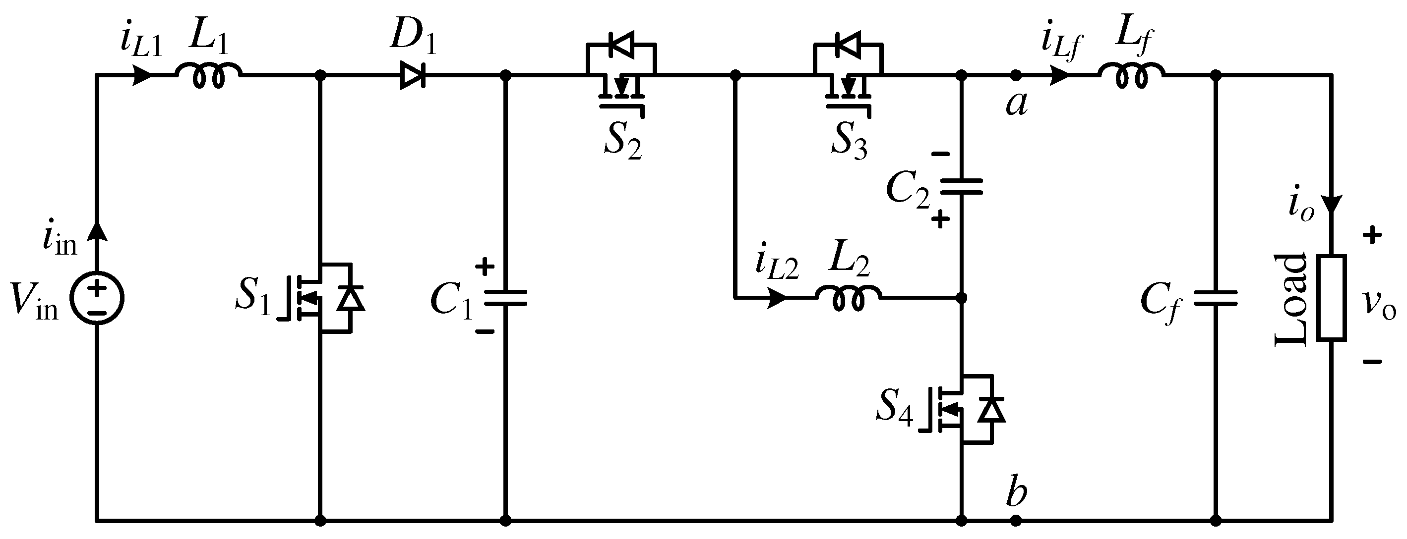
2. Principle Buck-Boost Bimodal Transformerless Inverter

2.1. Circuit Description

Figure 1 illustrates the circuit structure of the proposed single-stage buck-boost BTI (BB-BTI) with common-ground characteristics. A basic boost dc-dc converter is used to produce the single-polarity rectified sinusoidal voltage in the boost mode, and a BTI circuit is used to produce a sinusoidal voltage in the buck mode. The conventional boost dc-dc converter is built mainly by the power switches S1, the diode D1, and the inductor L1. The BTI includes the power switches S2, S3, and S4, the capacitor C2, and the inductor L2. Lf and Cf filter the voltage ripple of output voltage vo.
The operation principles of two-stage and single-stage BB-BTI are different. In a conventional two-stage BB-BTI, the switch S1 always operates at high frequency with the constant duty cycle so that the voltage on the DC-link capacitor is maintained at a set voltage value, which requires that the DC-link voltage is always greater than the output voltage. In addition, maintaining a constant DC-link voltage at high voltage requires a large capacitance value, which increases the DC-link capacitor’s size. In a proposed single-stage BB-BTI, the switch S1 only operates at high frequency when the input voltage is lower than the output voltage, the difference between the duty ratio of switch S1 in the proposed single-stage BB-BTI is constant, and in conventional two-stage BB-BTI is variant.

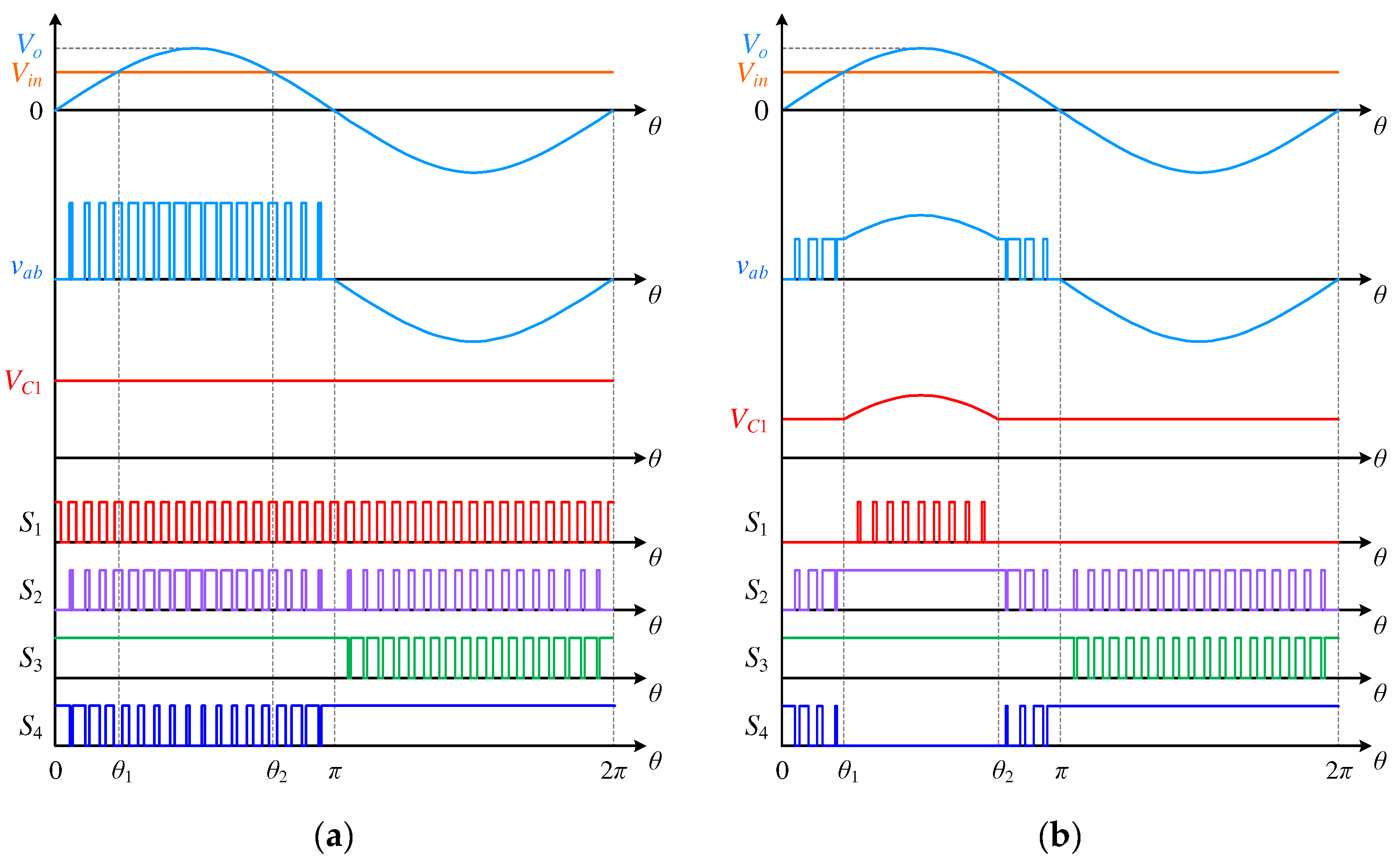
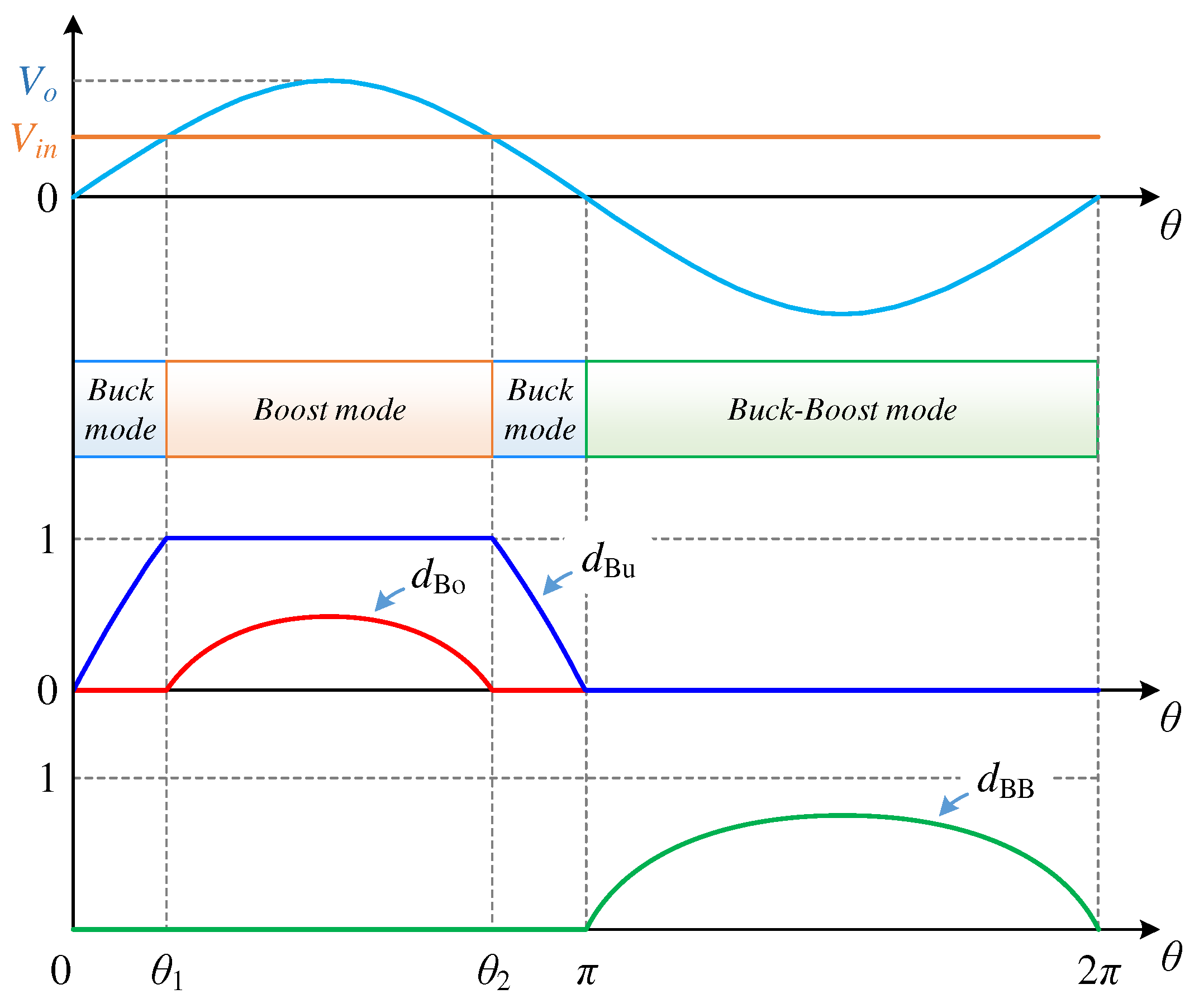
2.2. Operation Principles
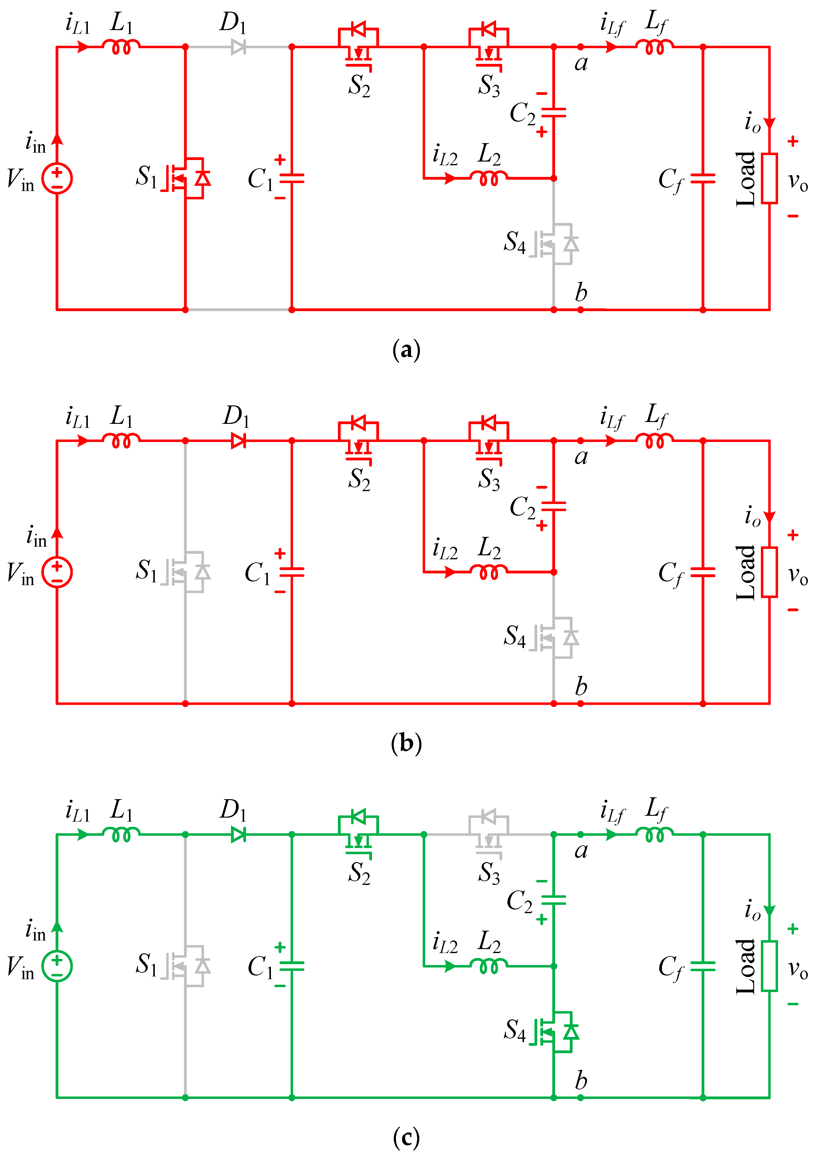
Figure 2 illustrates the key waveforms of the PWM strategy and control signals when the proposed single-stage BB-BTI operates with an input voltage Vin lower than the utility sine wave vo, where Vo is the magnitude of the voltage vo, Vin depicts the input voltage, VC1 is the voltage across capacitor C1, and vab is the inverter output voltage. In Figure 2a, the voltage across capacitor C1 is a straight line. In Figure 2b, the voltage of capacitor C1 is equal to the input voltage Vin and only varies between θ1 and θ2.
Besides, the states of S1 and S2 in Figure 2a change in the full cycle, while the state of S1 in Figure 2b changes only from θ1 to θ2, and S2 is kept ON from θ1 to θ2. The state of S4 in Figure 2a change from 0 to π, while the state of S4 in Figure 2b is kept OFF from θ1 to θ2.
The operating modes of the proposed single-stage BB-BTI can be divided into three modes, which include boost, buck, and buck-boost modes. The operating states of the proposed single-stage BB-BTI are shown in Figure 3.
  • Boost mode (θ1–θ2):
The states in boost mode are shown in Figure 3a,b. In this mode, the inductor is stored energy by the high-frequency operation of switch S1. The switches S2 and S3 are ON, and switch S4 is OFF. As can be seen in Figure 2b, the voltages across capacitor C1 have a curve shape, which has a peak value equal to the peak of the voltage vo. The inductor L2 current and capacitor C2 voltage are zero.
The switch S1 is ON. The diode D1 is reverse-biased. The inductor L1 is stored energy from the voltage Vin, and the current iL1 increases. The switches S2 and S3 are ON, and switch S4 is OFF. The capacitor C1 transferred energy to the load through switches S2 and S3, and Lf. The equations in this state can be written as:
L 1 d i L 1 d t = V i n L 2 d i L 2 d t = v C 2 L f d i L f d t = v C 1 v o
C 1 d v C 1 d t = i L f C 2 d v C 2 d t = i L 2 C f d v C f d t = i L f i o
The switches S1 and S4 are OFF. Inductor L1 and source connected in series. The diode D1 is forward-biased. The capacitor C1 and output load are supplied from inductor L1 and the input source. The voltage across the capacitor C1 is higher than the source voltage because of the additional voltage from the inductor L1, the current iL1 decreases. The related equations are as follows:
L 1 d i L 1 d t = V i n v C 1 L 2 d i L 2 d t = v C 2 L f d i L f d t = v C 1 v o
C 1 d v C 1 d t = i i n i L f C 2 d v C 2 d t = i L 2 C f d v C f d t = i L f i o
By considering the volt-second balance of inductors. vC1, vC2 is calculated as follows:
v C 1 = V i n 1 d B o v C 2 = 0
The output voltage in this mode is given as follows:
v o = V i n 1 d B o
where dBo denotes the duty cycle of switch S1.
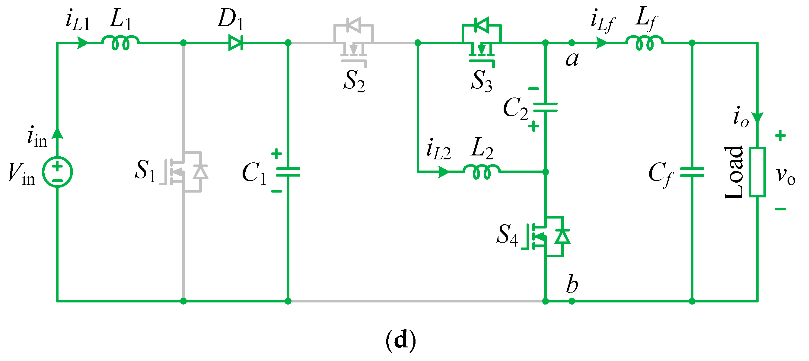
  • Buck mode (0–θ1 and θ2–π):
The states in Buck mode are shown in Figure 3b,d. The diode D1 is forward-biased, and the switch S1 is completely OFF. The voltages on C1 are equal to the input voltage. Both S2 and S4 operate at high-frequency. The current iL2 and voltage vC2 are zero.
In this case, the states of the switches are the same as state 2 in boost mode. However, the voltage of C1 is equal to voltage Vin, and the voltage of L1 is close to zero because switch S1 is OFF and the ripple voltage of C1 is small. The energy from the source is transferred to the output load. Switch S4 is OFF, and the voltages on capacitor C2 and inductor L2 are zero. The equations in this state are similar to Equations (3) and (4).
In this state, switches S1 and S2 are OFF and switches S3 and S4 are ON. The voltage on capacitor C1 is maintained at the input voltage through inductor L1 and diode D1, and the inverter output voltage is zero (vab = 0). The equations in this state can be derived as
L 1 d i L 1 d t = V i n v C 1 L 2 d i L 2 d t = v C 2 L f d i L f d t = v C 2 v o
C 1 d v C 1 d t = i i n C 2 d v C 2 d t = i L 2 + i L f C f d v C f d t = i L f i o
By applying the volt-second balance on inductors L1, L2, one can obtain,
v C 1 = V i n v C 2 = 0
The output voltage in this mode is given as follows:
v o = d B u V i n
where dBu is the duty cycle of switch S2 in the positive half cycle.
  • Buck-Boost mode (π–2π):
In Figure 3c,d, the states in buck-boost mode are shown. In this mode, the diode D1 is forward-biased, switch S1 is completely OFF, while switch S4 is completely ON. The voltages on C1 are equal to the input voltage. Both switches, S2 and S3, operate at high-frequency. The capacitor C2 is charged by the energy from inductor L2. The voltage of C2 is equal to the voltage vo.
Switches S1 and S3 are OFF and switches S2 and S4 are ON. The diode D1 is forward-biased, and the voltage of the capacitor C1 is equal to the input voltage. The inductor L2 is stored energy from the source and capacitor C1. The capacitor C2 discharges energy to the output load. The current through inductor L2 increases linearly. The differential equations are obtained as
L 1 d i L 1 d t = V i n v C 1 L 2 d i L 2 d t = v C 1 L f d i L f d t = v C 2 v o
C 1 d v C 1 d t = i i n i L 2 C 2 d v C 2 d t = i L f C f d v C f d t = i L f i o
This state is similar to state 2 in buck mode. However, in this state, the energy of the inductor L2 is non-zero. The inductor L2 supplies energy to the capacitor C2 and the output load. The current iL2 decreases linearly. The differential equations are obtained as
L 1 d i L 1 d t = V i n v C 1 L 2 d i L 2 d t = v C 2 L f d i L f d t = v C 2 v o
C 1 d v C 1 d t = i i n C 2 d v C 2 d t = i L 2 + i L f C f d v C f d t = i L f i o
By applying the volt-second balance on inductors L1 and L2. The equations of this mode are derived as follows:
v C 1 = V i n v C 2 = V o
The output voltage is given as follows:
v o = d B B V i n d B B 1
where dBB is the duty cycle of switch S2 in the negative half cycle.
The output voltage and the modulation index (M) of the proposed single-stage BTI are supposed to be
v o = V o s i n θ
M = V o V i n
As visualized in Figure 4. The resulting duty cycles of the proposed single-stage BTI are calculated based on (18) as
d B o = 0 ,   0 < θ θ 1   a n d   θ 2 < θ 2 π   1 1 M s i n θ , θ 1 < θ θ 2
d B u = M s i n θ ,   0 < θ θ 1   a n d   θ 2 < θ π 1 , θ 1 < θ θ 2   0 ,   π < θ 2 π
d B B =   0 ,   0 < θ π M s i n θ M s i n θ 1 , π < θ 2 π
The transition angles from boost mode to buck mode are given by
θ 1 = s i n 1 1 M   θ 2 = π s i n 1 1 M , M 1
From (19)–(21), the maximum values of the duty cycles can be calculated as follows:
D B o . m a x = M 1 M ,   M > 1 0 ,   M 1
D B u . m a x = 1 ,   M 1 M ,   M < 1
D B B . m a x = M M + 1
Figure 4 shows the dBo, dBu, and dBB of BB-BTI for a peak output voltage of 156 V and an input voltage of Vin of 80 V. For vo > Vin, dBo varies from 0 at vo = 80 V to 0.487 at vo = 156 V. For vo < Vin, dBu varies from 0 at vo = 0 V to 1 at vo = 80 V, and for vo < 0, dBB varies from 0 at vo = −156 V to 0.66 at vo = −156 V.

3. Component Selection

3.1. Inductor

Regarding (2), (4), (8), (12), and (14), the inductor currents, iL1 and iL2, can be expressed as:
i L 1 = i o d B u , 0 < θ θ 1   a n d   θ 2 < θ π   i o 1 d B o ,   θ 1 < θ θ 2 i o d B B d B B 1 ,   π < θ 2 π
i L 2 = i o d B u 1 , 0 < θ θ 1   a n d   θ 2 < θ π   0 ,   θ 1 < θ θ 2 i o d B B 1 , π < θ 2 π
According to (20), (21), (26), and (27), the current of the inductors, L1 and L2, are given as follows:
i L 1 = I o M s i n 2 θ
i L 2 = I o M s i n 2 θ I o s i n θ , 0 < θ θ 1   a n d   θ 2 < θ 2 π 0 ,   θ 1 < θ θ 2
The high-frequency inductor current ripple can be considered as follows:
i L 1 = V i n d B o L 1 f s
i L 2 = V i n d B B L 2 f s
By replacing (19) and (21) with (30) and (31), we can also write
i L 1 = M 1 V i n M L 1 f s
i L 2 = M V i n M + 1 L 2 f s
The final value of L1, and L2 are designed as:
L 1 = M 1 V i n M f s i L 1
L 2 = M V i n M + 1 f s i L 2

3.2. Capacitor

Using (5), (9), and (15), the voltage of capacitors C1 and C2 can be derived
v C 1 = V i n , 0 < θ θ 1   a n d   θ 2 < θ 2 π   v o ,   θ 1 < θ θ 2
v C 2 = 0 ,   0 < θ π v o , π < θ 2 π
The ripple voltage of the capacitors C1 and C2 can be written as:
v C 1 = i o d B o C 1 f s , v o > 0 i o d B B C 1 f s , v o < 0
v C 2 = i o d B B C 2 f s
Maximum values of ΔvC1 and ΔvC2 are achieved when dBB = DBB.max (θ = 3π/2). The capacitance of the capacitors can be expressed as:
v C 1 = M I o M + 1 C 1 f s
v C 2 = M I o M + 1 C 2 f s
The value of the capacitors C1 and C2 can be expressed as
C 1 = M I o M + 1 v C 1 f s
C 2 = M I o M + 1 v C 2 f s

3.3. Switches and Diode

The drain-source voltages of switches are given as follows:
V S 1 = V S 4 = V D 1 = V o V S 2 = V S 3 = V i n + V o
The currents of switches are given as
I S 1 = I D 1 = M I o I S 2 = I S 3 = M + 1 I o I S 4 = M + 2 I o

4. Comparison

4.1. Comparison with the Two-Stage Bimodal Inverter

Table 1 demonstrates the comparison between the conventional two-stage BB-BTI and the proposed single-stage BB-BTI. The proposed single-stage BB-BTI requires three small capacitors, while the conventional two-stage BB-BTI needs two small and one bulky capacitor. For a better comparison, the voltage stress for switches and capacitors is calculated. The specific results for M = 1.95 for conventional two-stage BB-BTI and proposed single-stage BB-BTI are shown in Table 2. From Table 2, the maximum voltage stress on switches of conventional two-stage BB-BTI equal 2.16Vo, while this stress is limited to 1.51Vo for the proposed single-stage BB-BTI. In addition, the voltage stress across capacitors of the conventional two-stage BB-BTI reaches to 1.16Vo, while this stress in the proposed single-stage BB-BTI is limited to Vo. Therefore, the proposed single-stage BB-BTI can be implemented with switches and capacitors of significantly lower voltage. Consequently, the costs are decreased in the proposed single-stage BB-BTI compared to the conventional two-stage BB-BTI.

4.2. Comparison with Other Buck-Boost Common-Ground Inverters

To show the potential of the proposed single-stage BB-BTI, a comparison with other inverters has been summarized in Table 3. Comparison criteria such as the number of diodes, switches, capacitors, inductors, the total number of devices, voltage stress across diodes and switches, total standing voltage (TSV) [35] and the presented efficiency. The common-ground-type transformerless inverter in [23] has the least total number of devices, and the number of switches and diodes is equal to the proposed single-stage BB-BTI. However, this topology requires an input voltage greater than the output voltage. Besides, a large value capacitor is required to generate a voltage in the negative half of the output, which is also a disadvantage.
The inverters presented in [30,31] have the same total number of devices; the topology presented in [30] uses one more diode and one switch than the proposed single-stage BB-BTI. The single-stage bidirectional buck-boost inverters in [31] use only an inductor and do not use diodes, but two input sources or two large capacitors are required. In [32], the topology uses the most number of switches, there are four switches with voltage stress reaches (Vin + Vo), and two inductors are used. However, the leakage current is not completely eliminated. The topology presented in [33] uses the most diodes; the diodes and switches in this structure all have a voltage of (Vin + Vo), so the inverter loss is high. The topology presented in [29] includes two boost and one buck converter. However, this topology uses more than two diodes and one switch, which makes the total components of this topology much more than the proposed single-stage BB-BTI. In addition, the proposed single-stage BB-BTI has a lower TSV and efficiency compared to other studies. Through the comparison required in Table 3, the proposed single-stage BB-BTI has shown outstanding advantages such as the low number of components, small capacitors and buck-boost capability.

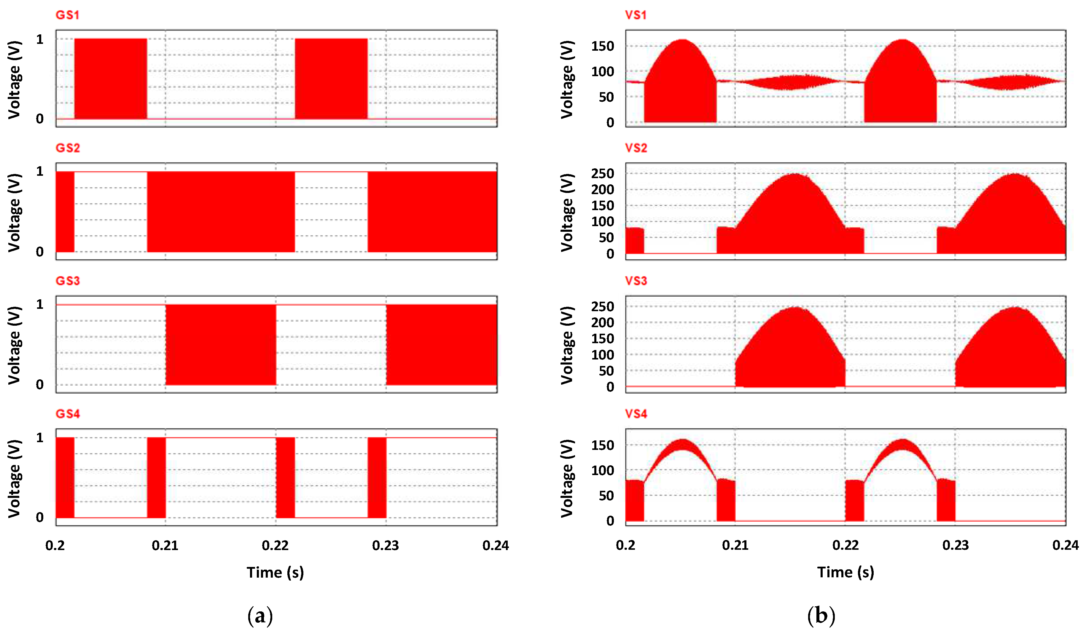
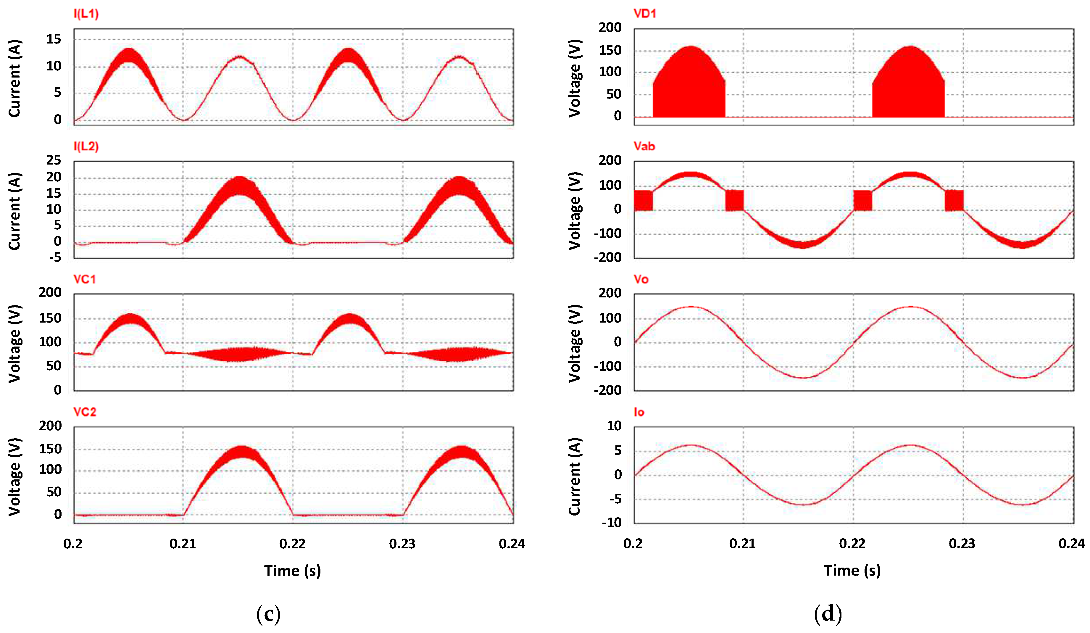
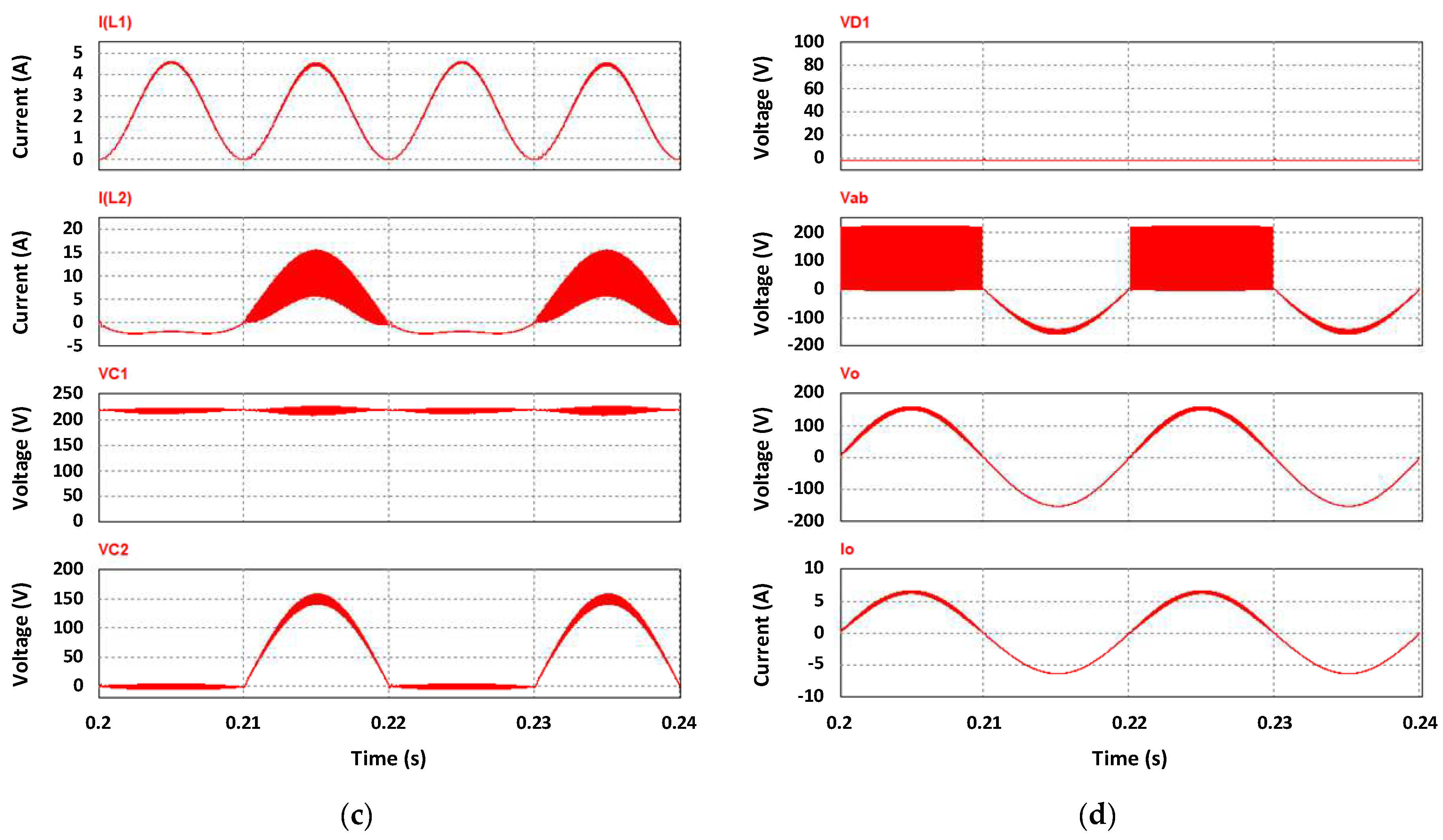
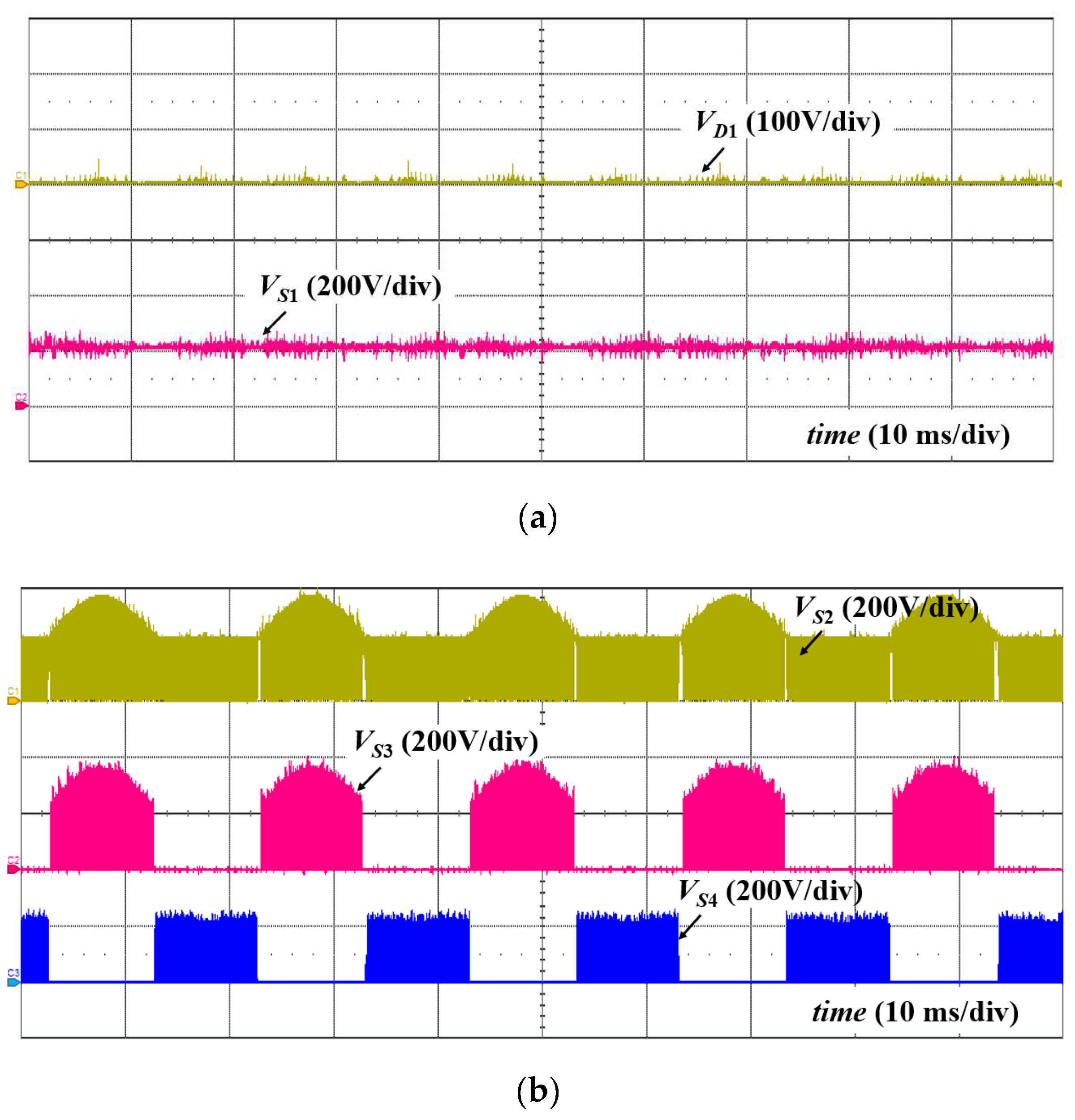
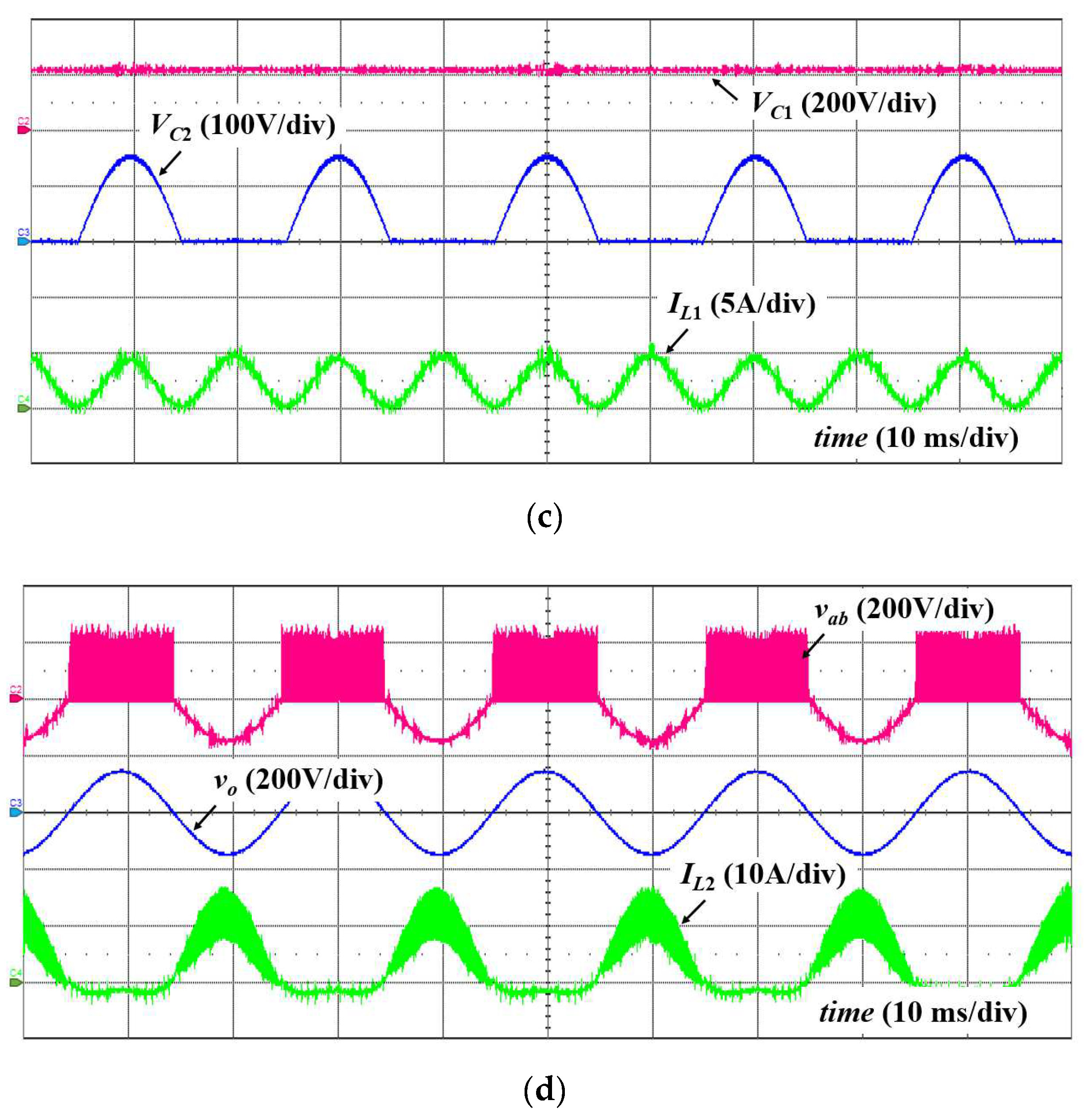
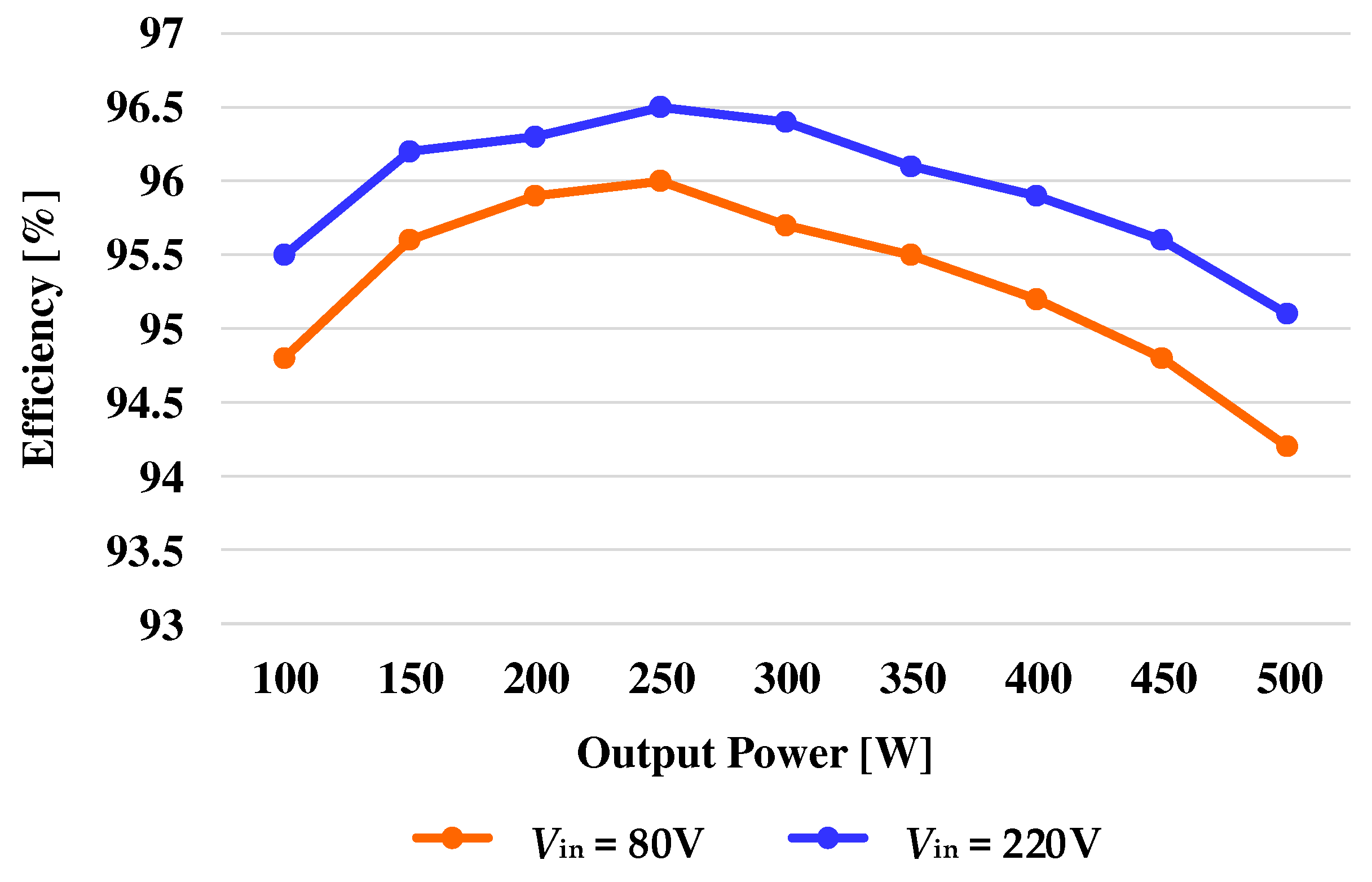
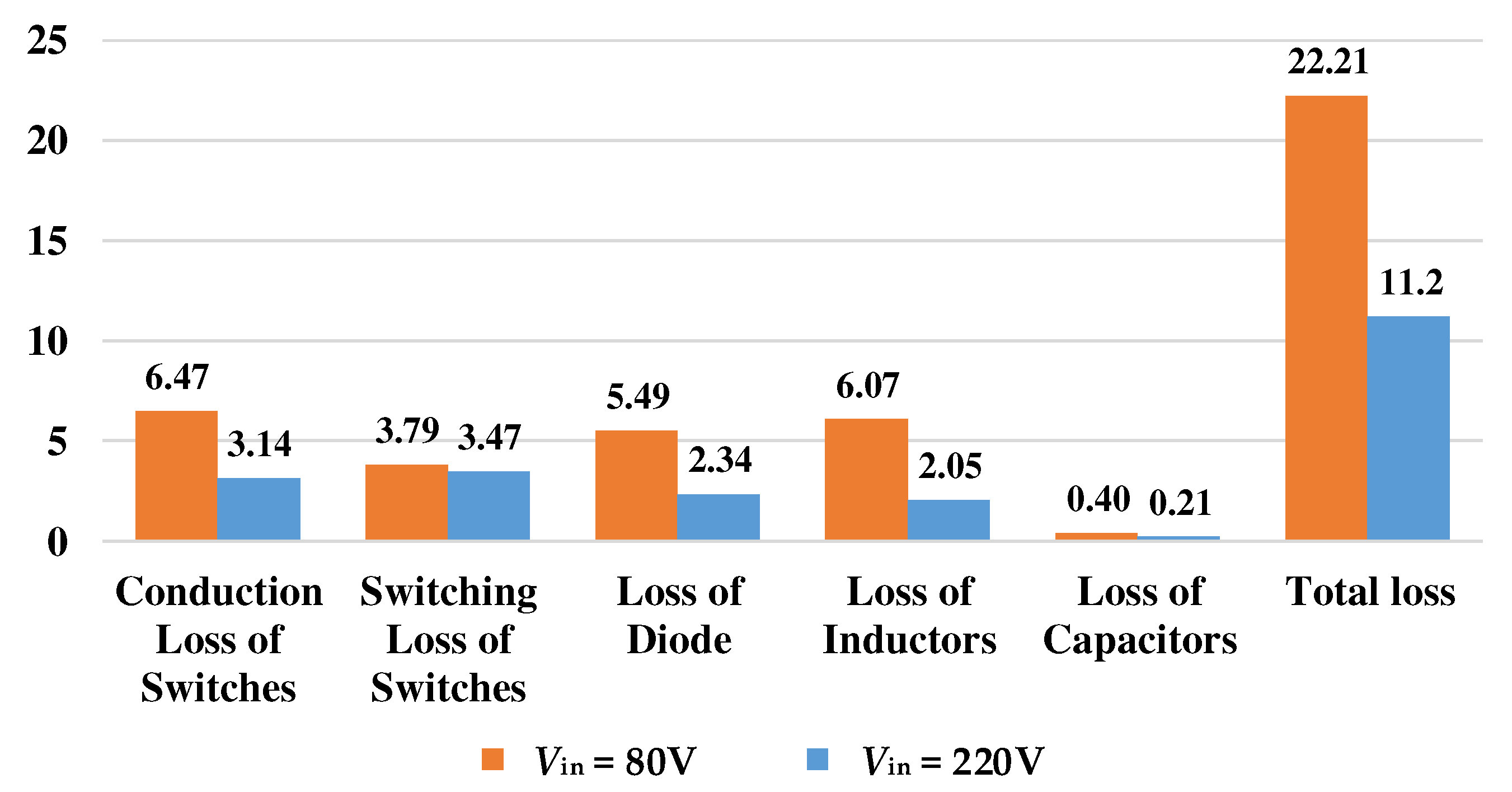
5. Simulation and Experimental Results

5.1. Simulation Results

Simulations were conducted using PSIM 9.1.1 (Troy, MI, USA) to verify the operation of the proposed single-stage BB-BTI. The parameters for the simulation are L1 = 0.5 mH, L2 = 0.3 mH, Lf = 0.3 mH, C1 = 5 μF, C2 = 5 μF, Cf = 2 μF, and R = 24 Ω. The output frequency and switching frequency are set at 50 Hz and 30 kHz, respectively. The forward voltage of diode D1 is 1 V. The drain-to-source on-resistance of switches S1 and S4 are 25.5 mΩ, and for S2, S3 are 45 mΩ.
Figure 5 and Figure 6 show the simulation results when Vin = 80 V and Vin = 220 V, respectively. In Figure 5a and Figure 6a, the driving waveform of switches S1S4 is shown. Figure 5b and Figure 6b show the voltages stress across switches S1S4. Figure 5b and Figure 6b show the current of inductors L1 and L2 and the voltage across capacitors C1 and C2. In Figure 5d and Figure 6d, the waveforms in this figures are the voltage of diode D1, the inverter output voltage, vab, the output voltage, vo, and the output current, io.

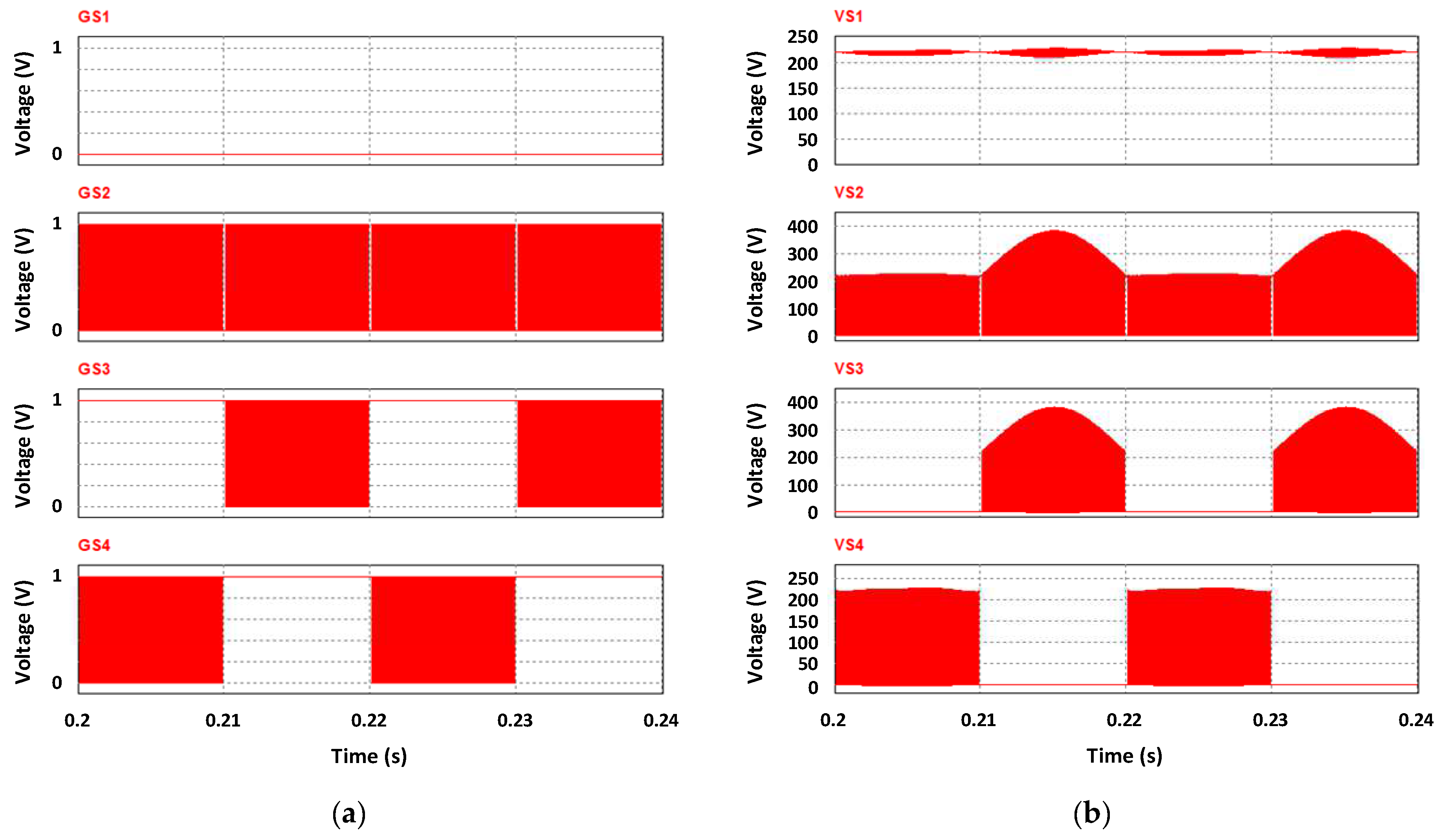
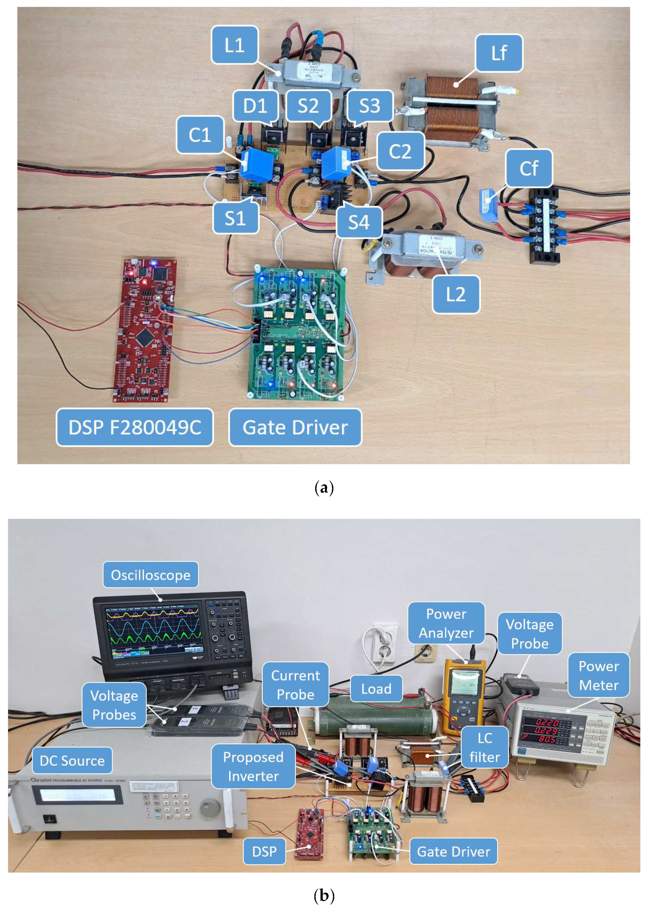
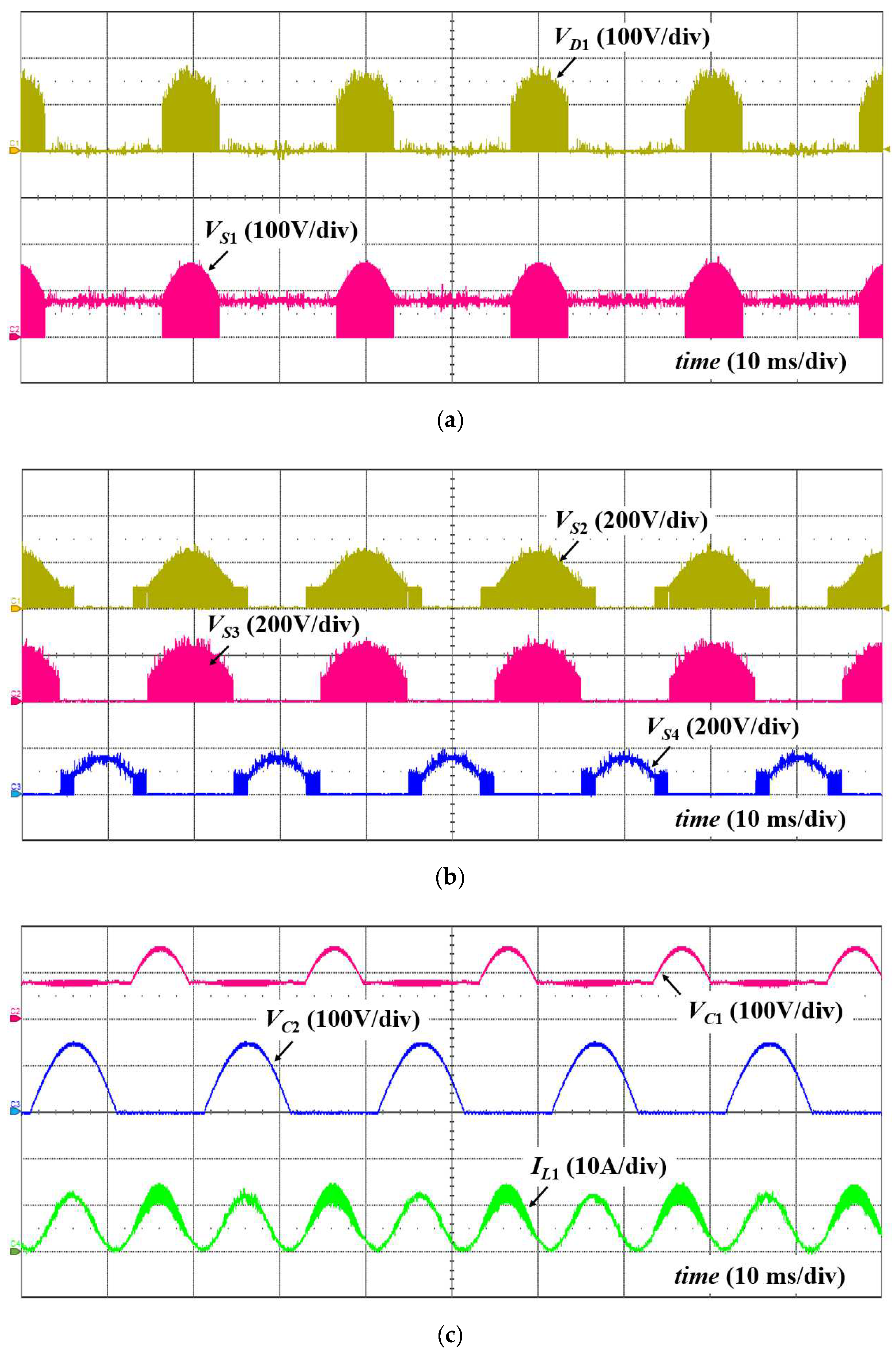
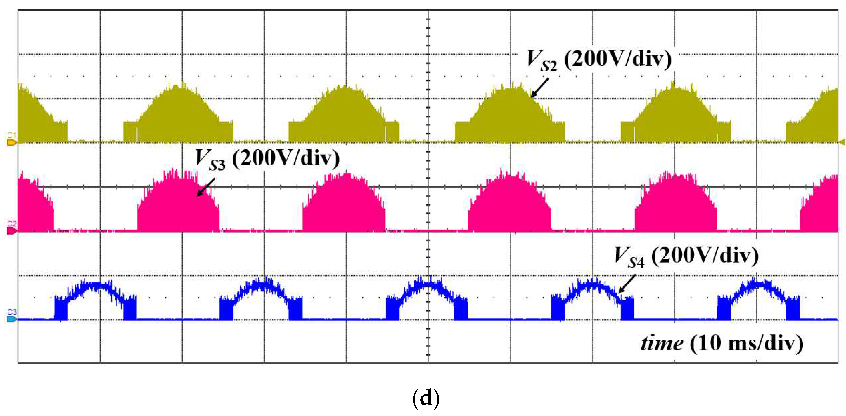
5.2. Experiment Results

To further validate the proposed single-stage BB-BTI analysis and its control, a 500 W concept-proof laboratory prototype is illustrated in Figure 7 with the components detailed in Table 4. The control platform is DSP F280049C. Chroma 61604 provides dc power. The input and output powers are measured by the WT230 Digital Power Meter. The output current harmonics are measured by Fluke 43 B. The load resistance of 25 Ω (where two resistors of 50 Ω in parallel) was used as the output load.
As shown in Figure 8, the experimental results with Vin = 80 V and the modulation index M = 1.95. Figure 8a indicates the voltage of the diode D1 and the voltage of the switch S1. Figure 8b shows the voltage of switches S2, S3, and S4. The peak voltage of D1, S4, and S1 are about 156 V. The peak voltages of S2 and S3 are about 235 V. Figure 8c illustrates the voltage of capacitors C1 and C2 and the current through the inductor L1. The voltage stress of capacitors is about 155 V. The current through the inductor L1 varies from 0 to 14 A, and the average current of the inductor L1 is 6.1 A. Figure 8d shows the output voltages vab, vo, and current through the inductor L2. The THD values of the output voltage vo are 1.82%. The average current through the inductor L2 is 5.02 A, and the peak current is about 22 A.
Figure 9 shows the experimental results with Vin = 220 V, corresponding to the modulation index M = 0.71. As shown in Figure 9a,b, the voltage stress on S1 and S4 is equal to the input voltage. The voltage stress on S2 and S3 is equal to the sum of the input and output voltages. Figure 9c shows the voltage of capacitors C1 and C2 and the current through the inductor L1. The average current of the inductor L1 is 2.35A. As indicated in Figure 9d, the output voltages vab, vo, and current through the inductor L2. The THD value of the output voltage vo is 1.1%. The average current through the inductor L2 is 2.32 A, and the peak current is about 16 A.
As indicated in Figure 10, the efficiency of the proposed single-stage BB-BTI in case of input voltage at 80 V and 220 V, the output voltage is considered at 110 Vrms. The efficiency results show that the efficiency when the input voltage is 80 V is lower than the input voltage of 220 V. The peak efficiencies are 96% and 96.5% at 80 V and 220 V, respectively.
The distribution of power loss of the proposed single-stage BB-BTI based on the parameters shown in Table 4 is shown in Figure 11.

6. Conclusions

This paper presented the proposed single-phase, single-stage BB-BTI. The proposed inverter provides common ground and buck-boost capability. Compared with the conventional two-stage BB-BTI, the proposed single-stage BB-BTI has lower voltage stress on the switches and capacitors. Furthermore, the switching operation in the proposed single-stage BB-BTI is significantly less than in conventional two-stage BB-BTI, thereby improving efficiency and reducing filter inductor. The circuit does not contain an electrolytic capacitor, which reduces the volume and improves the life of the inverter. Mathematical analysis, design consideration, and comparison with existing common-ground single-phase inverters were performed. Finally, the simulation and experimental results were presented to confirm the performance of the proposed single-stage BB-BTI.

Author Contributions

D.-V.V. determined topology, original draft preparation, and contributed to validating in simulation and experimental works; K.M.N. contributed to the review and editing; Y.-C.L. provided resources and supervision; J.-H.C. provided resources and funding acquisition. All authors have read and agreed to the published version of the manuscript.

Funding

This research received no external funding.

Institutional Review Board Statement

Not applicable.

Informed Consent Statement

Not applicable.

Data Availability Statement

Data are contained within the article.

Conflicts of Interest

The authors declare no conflict of interest.

References

  1. Jo, K.Y.; Duong, T.D.; Choi, J.-H. Emerging technologies in power systems. Electronics 2022, 11, 71. [Google Scholar] [CrossRef]
  2. Can, E. The design and experimentation of the new cascaded DC-DC boost converter for renewable energy. Int. J. Electron. 2019, 106, 1374–1393. [Google Scholar] [CrossRef]
  3. Can, E. A new multi-level inverter with reverse connected dual dc to dc converter at simulation. Int. J. Model. Simul. 2022, 42, 34–46. [Google Scholar] [CrossRef]
  4. Duong, T.D.; Nguyen, M.K.; Tran, T.T.; Choi, J.H.; Lim, Y.C. Transformerless High Step-Up DC-DC Converters with Switched-Capacitor Network. Electronics 2019, 8, 1420. [Google Scholar] [CrossRef] [Green Version]
  5. Duong, T.D.; Nguyen, M.K.; Nguyen, T.T.; Cha, H.; Lim, Y.C.; Choi, J.H. Switching-Cell Structure Based Generic Five-Level Current Source Inverter. IEEE Trans. Ind. Electron. 2022, 1–10. [Google Scholar] [CrossRef]
  6. Alluhaybi, K.; Batarseh, I.; Hu, H. Comprehensive review and comparison of single-phase grid-tied photovoltaic microinverters. IEEE J. Emerg. Sel. Top. Power Electron. 2020, 8, 1310–1329. [Google Scholar] [CrossRef]
  7. Li, W.; Gu, Y.; Luo, H.; Cui, W.; He, X.; Xia, C. Topology review and derivation methodology of single-phase transformerless photovoltaic inverters for leakage current suppression. IEEE Trans. Ind. Electron. 2015, 62, 4537–4551. [Google Scholar] [CrossRef]
  8. Duong, T.D.; Nguyen, M.K.; Tran, T.-T.; Vo, D.-V.; Lim, Y.C.; Choi, J.-H. Topology Review of Three Phase Two-Level Transformerless Photovoltaic Inverters for Common-Mode Voltage Reduction. Energies 2022, 15, 3106. [Google Scholar] [CrossRef]
  9. Nguyen, M.K.; Duong, T.D.; Lim, Y.C.; Choi, J.H. High voltage gain quasi-switched boost inverters with low input current ripple. IEEE Trans. Ind. Inform. 2019, 15, 4857–4866. [Google Scholar] [CrossRef]
  10. Vo, D.-V.; Nguyen, M.-K.; Do, D.-T.; Choi, Y.-O. A Single-Phase Nine-Level Boost Inverter. Energies 2019, 12, 394. [Google Scholar] [CrossRef]
  11. Tran, T.T.; Nguyen, M.K.; Duong, T.D.; Choi, J.H.; Lim, Y.C.; Zare, F. A Switched-Capacitor Voltage-Doubler Based Boost Inverter for Common-Mode Voltage Reduction. IEEE Access 2019, 7, 98618–98629. [Google Scholar] [CrossRef]
  12. Duong, T.D.; Nguyen, M.K.; Tran, T.T.; Lim, Y.C.; Choi, J.H.; Wang, C. Modulation techniques for modified three-phase quasi-switched boost inverter with common-mode voltage reduction. IEEE Access 2020, 7, 160670–160683. [Google Scholar] [CrossRef]
  13. Tai, T.T.; Nguyen, M.K.; Duong, T.D.; Lim, Y.C.; Choi, J.H. A switched-capacitor-based six-level inverter. IEEE Trans. Power Electron. 2022, 37, 4804–4816. [Google Scholar]
  14. Liu, C.; Wang, Y.; Cui, J.; Zhi, Y.; Liu, M.; Cai, G. Transformerless photovoltaic inverter based on interleaving high-frequency legs having bidirectional capability. IEEE Trans. Power Electron. 2016, 31, 1131–1142. [Google Scholar] [CrossRef]
  15. Wang, L.; Shi, Y.; Shi, Y.; Xie, R.; Li, H. Ground leakage current analysis and suppression in a 60-kW 5-Level T-Type transformerless SiC PV inverter. IEEE Trans. Power Electron. 2018, 33, 1271–1283. [Google Scholar] [CrossRef]
  16. Guo, X. Three-phase CH7 inverter with a new space vector modulation to reduce leakage current for transformerless photovoltaic systems. IEEE J. Emerg. Sel. Top. Power Electron. 2017, 5, 708–712. [Google Scholar] [CrossRef]
  17. Yang, B.; Li, W.; Gu, Y.; Cui, W.; He, X. Improved transformerless inverter with common-mode leakage current elimination for a photovoltaic grid-connected power system. IEEE Trans. Power Electron. 2012, 27, 752–762. [Google Scholar] [CrossRef]
  18. Kerekes, T.; Teodorescu, R.; Rodríguez, P.; Vázquez, G.; Aldabas, E. A new high-efficiency single-phase transformerless PV inverter topology. IEEE Trans. Ind. Electron. 2011, 58, 184–191. [Google Scholar] [CrossRef] [Green Version]
  19. Dong, H.; Xie, X.; Jiang, L.; Jin, Z.; Zhao, X. An electrolytic capacitor-less high power factor LED driver based on a ‘one-and-a-half stage’ forward-flyback topology. IEEE Trans. Power Electron. 2018, 33, 1572–1584. [Google Scholar] [CrossRef]
  20. Tian, K.; Wu, B.; Narimani, M.; Xu, D.; Cheng, Z.; Zargari, N.R. A capacitor voltage-balancing method for nested neutral point clamped (NNPC) inverter. IEEE Trans. Power Electron. 2016, 31, 2575–2583. [Google Scholar] [CrossRef]
  21. Tang, Y.; Yao, W.; Loh, P.C.; Blaabjerg, F. Highly reliable transformerless photovoltaic inverters with leakage current and pulsating power elimination. IEEE Trans. Ind. Electron. 2016, 63, 1016–1026. [Google Scholar] [CrossRef]
  22. Gu, Y.; Li, W.; Zhao, Y.; Yang, B.; Li, C.; He, X. Transformerless inverter with virtual DC bus concept for cost-effective grid-connected PV power systems. IEEE Trans. Power Electron. 2013, 28, 793–805. [Google Scholar] [CrossRef]
  23. Siwakoti, Y.P.; Blaabjerg, F. Common-Ground-Type Transformerless Inverters for Single-Phase Solar Photovoltaic Systems. IEEE Trans. Ind. Electron. 2018, 65, 2100–2111. [Google Scholar] [CrossRef]
  24. Ardashir, J.F.; Sabahi, M.; Hosseini, S.H.; Blaabjerg, F.; Babaei, E.; Gharehpetian, G.B. A single-phase transformerless inverter with charge pump circuit concept for grid-tied PV applications. IEEE Trans. Ind. Electron. 2017, 64, 5403–5414. [Google Scholar] [CrossRef]
  25. Zhu, X.; Zhang, B.; Qiu, D. A new half-bridge impedance source inverter with high voltage gain. IEEE Trans. Power Electron. 2019, 34, 3001–3008. [Google Scholar] [CrossRef]
  26. Kim, K.; Cha, H.; Kim, H. A new single-phase switched-coupled-inductor DC–AC inverter for photovoltaic systems. IEEE Trans. Power Electron. 2017, 32, 5016–5022. [Google Scholar] [CrossRef]
  27. Sarikhani, A.; Takantape, M.M.; Hamzeh, M. A Transformerless Common-Ground Three-Switch Single-Phase Inverter for Photovoltaic Systems. IEEE Trans. Power Electron. 2020, 35, 8902–8909. [Google Scholar] [CrossRef]
  28. Vo, D.-V.; Nguyen, M.-K.; Duong, T.-D.; Tran, T.-T.; Lim, Y.-C.; Choi, J.-H. A Novel Single-Stage Common-Ground Transformerless Buck–Boost Inverter. Electronics 2022, 11, 829. [Google Scholar] [CrossRef]
  29. Yao, Z.; Wang, Z. Single-Stage Doubly Grounded Transformerless PV Grid-Connected Inverter with Boost Function. IEEE Trans. Power Electron. 2022, 37, 2237–2249. [Google Scholar] [CrossRef]
  30. Karschny, D. Flying Inductor Topology. DE 196 42 522 C1, 23 April 1998. [Google Scholar]
  31. Khan, A.A.; Lu, Y.W.; Eberle, W.; Wang, L.; Khan, U.A.; Agamy, M.; Cha, H. Single-Stage Bidirectional Buck–Boost Inverters Using a Single Inductor and Eliminating the Common-Mode Leakage Current. IEEE Trans. Power Electron. 2020, 35, 1269–1281. [Google Scholar] [CrossRef]
  32. Ho, C.N.M.; Siu, K.K.M. Manitoba Inverter—Single-Phase Single Stage Buck-Boost VSI Topology. IEEE Trans. Power Electron. 2019, 34, 3445–3456. [Google Scholar] [CrossRef]
  33. Ahmed, H.F.; El Moursi, M.S.; Zahawi, B.; Al Hosani, K. Single-Phase Photovoltaic Inverters with Common-Ground and Wide Buck–Boost Voltage Operation. IEEE Trans. Ind. Inform. 2021, 17, 8275–8287. [Google Scholar] [CrossRef]
  34. Liu, Y.; Zhou, Y.; Guo, B.; Wang, H.; Su, M.; Liang, X.; Pan, X. Bimodal Transformerless Inverter with Three Switches. IEEE Trans. Ind. Electron. 2022, 69, 8972–8983. [Google Scholar] [CrossRef]
  35. Gupta, K.K.; Ranjan, A.; Bhatnagar, P.; Sahu, L.K.; Jain, S. Multilevel inverter topologies with reduced device count: A review. IEEE Trans. Power Electron. 2016, 31, 135–151. [Google Scholar] [CrossRef]
Figure 1. The proposed single-phase BB-BTI.
Electronics 12 00221 g001
Figure 2. PWM control method for (a) conventional two-stage BB-BTI and (b) the proposed single-stage BB-BTI.
Electronics 12 00221 g002
Figure 3. Circuit states of the proposed single-stage BB-BTI. (a) State 1 of boost mode, (b) State 2 of boost mode, and state 1 of buck mode, (c) State 1 of buck-boost mode, (d) State 2 of buck and buck-boost modes.
Electronics 12 00221 g003aElectronics 12 00221 g003b
Figure 4. Variation of the duty cycles with the output voltage of the proposed single-stage BB-BTI.
Electronics 12 00221 g004
Figure 5. Simulation results for the proposed single-stage BB-BTI when Vin = 80 V. (a) Control signals of S1, S2, S3, and S4. (b) Voltages VS1, VS2, VS3, and VS4. (c) currents iL1, iL2, and voltages vC1, vC2. (d) Voltages VD1, vab, and vo, and current io.
Electronics 12 00221 g005aElectronics 12 00221 g005b
Figure 6. Simulation results for the proposed single-stage BB-BTI when Vin = 220 V. (a) Control signals of S1, S2, S3, and S4. (b) Voltages VS1, VS2, VS3, and VS4. (c) currents iL1, iL2, and voltages vC1, vC2. (d) Voltages VD1, vab, and vo, and current io.
Electronics 12 00221 g006aElectronics 12 00221 g006b
Figure 7. Photo of the laboratory prototype. (a) Prototype. (b) Measurement setup.
Electronics 12 00221 g007
Figure 8. Experimental results with Vin = 80 V. (a) Diode D1 and switch S1 voltage. (b) Switches S2, S3, S4 voltage. (c) Capacitors C1, C2 voltage, and inductor L1 current. (d) inverter output voltage vab, load voltage vo, and inductor L2 current.
Electronics 12 00221 g008aElectronics 12 00221 g008b
Figure 9. Experimental results with Vin = 220 V. (a) Diode D1 and switch S1 voltage. (b) Switches S2, S3, S4 voltage. (c) Capacitors C1, C2 voltage, and inductor L1 current. (d) inverter output voltage vab, load voltage vo, and inductor L2 current.
Electronics 12 00221 g009aElectronics 12 00221 g009b
Figure 10. Measured experimental efficiency.
Electronics 12 00221 g010
Figure 11. Distribution of power loss.
Electronics 12 00221 g011
Table 1. Comparison of conventional two-stage BB-BTI with the proposed single-stage BB BTI.
Voltage StressConventional Two-Stage BB BTIProposed Single-Stage BB BTI
S1, S4 1 M 1 d B o V o Vo
S2, S3 1 + M 1 d B o M 1 d B o V o M + 1 M V o
C1 1 M 1 d B o V o Vo
C2VoVo
Table 2. Comparison of conventional two-stage BB-BTI with the proposed single-stage BB-BTI with the same modulation index.
Voltage StressTwo-Stage BB BTI
(M = 1.95, dBo = 0.56)
Proposed Single-Stage BB BTI
(M = 1.95, DBo.max = 0.487)
S1, S41.16VoVo
S2, S32.16Vo1.51Vo
C11.16VoVo
C2VoVo
Table 3. Comparison between the proposed single-stage BB-BTI and other common-ground transformerless inverters.
Topology[23][30][31][32][33][29]Proposed
BB-BTI
Diodes1200431
Switches4568554
Capacitors2131223
Inductors1212433
Total Devices8101011151311
Diodes stressD1: VinD1: Vin + Vo
D2: Vo
--D1D4: Vin + VoD1: Vo
D2: Vin + Vo
D3:Vo-Vin
D1: Vo
Switches stressS1S4: VinS1: Vin + Vo
S2S5: Vo
S1, S2: Vin
S3S6: Vin + Vo
S1S4: Vin + Vo
S5S8: Vo
S1S5: Vin + VoS1, S2: Vin + Vo
S3S5: Vo
S1, S4: Vo
S2, S3: Vin + Vo
TSV4Vin1Vin + 5Vo6Vin + 4Vo4Vin + 8Vo5Vin + 5Vo2Vin + 5Vo2Vin + 4Vo
PresentedEfficiency99.2%
@1kW
-95.9%
@0.4kW
95.7%
@0.8kW
96.74%
@0.4kW
97.1%
@0.45kW
96.5%
@0.5kW
Table 4. Parameters for the experiment.
ParameterSymbolValue
Input voltage Vin80–220 V
Output voltagevo110 Vrms
Output frequencyfo50 Hz
Switching frequencyfs30 kHz
Output powerPo500 W
DiodeD1STTH6003 (300 V, 60 A, VF = 1 V)
SwitchesS1, S4IRFP4868PbF (300V, 70 A, Rdson = 25.5 mΩ)
S2, S3IPW60R045CPA (600 V, 60 A, Rdson = 45 mΩ)
InductorsL10.5 mH
L2, Lf0.3 mH
CapacitorsC1, C25 µF
Cf2 µF
Disclaimer/Publisher’s Note: The statements, opinions and data contained in all publications are solely those of the individual author(s) and contributor(s) and not of MDPI and/or the editor(s). MDPI and/or the editor(s) disclaim responsibility for any injury to people or property resulting from any ideas, methods, instructions or products referred to in the content.

