Article

A Reconfigurable Hybrid RF Front-End Rectifier for Dynamic PCE Enhancement of Ambient RF Energy Harvesting Systems

1
Department of Electrical Engineering, Faculty of Engineering, University of Malaya, Kuala Lumpur 50603, Malaysia
2
Nexperia R&D Penang, Bayan Lepas 11900, Malaysia
3
Centre of Research Industry 4.0 (CRI 4.0), Faculty of Engineering, University of Malaya, Kuala Lumpur 50603, Malaysia
4
State-Key Laboratory of Analog and Mixed-Signal VLSI and IME/ECE-FST, University of Macau, Macau 999078, China
5
Insitituto Superior Técnico, Universidade de Lisboa, 1649-004 Lisboa, Portugal
*
Author to whom correspondence should be addressed.
Electronics 2023, 12(1), 175; https://doi.org/10.3390/electronics12010175
Submission received: 30 November 2022 / Revised: 23 December 2022 / Accepted: 26 December 2022 / Published: 30 December 2022

Abstract

:
This paper presents a reconfigurable hybrid Radio Frequency (RF) rectifier designed to efficiently convert AC RF power to DC voltages for an energy harvesting system. The proposed reconfigurable rectifier adopts the advantage of low conduction loss in the switch-connected rectifier and low reverse current loss in the diode-connection rectifier topology to enhance its power conversion efficiency (PCE). Capable of reconfiguring into different rectifier topologies, the proposed circuit can reconfigure into a switch-based cross-coupling differential drive (CCDD) at low input power and a diode-based hybrid rectifier at higher input power for a wide dynamic range operation. Designed and implemented on a CMOS 65 nm technology, the post-layout result records a peak PCE of 88.7% and a wide PCE dynamic range (PDR) of 16 dBm for PCE >40%. The proposed circuit also demonstrates a −21 dBm sensitivity output across a 1 MΩ output load.

1. Introduction

With the increasing demand for self-powered autonomous sensors for the Internet of Things (IoT), energy harvesting will become a key enabling technology with widespread deployment. The uprising of radiofrequency (RF) has enabled widespread wireless communication in many environments, such as in urban cities, offices, and homes. Due to this, the opportunity to harvest the available RF energy in the environment presents a new form of energy source in the upcoming IoT growth.
Integrating miniaturized sensors through complementary integrated circuits to harvest ambient RF energy adds to challenges. The varying nature of ambient RF, nonuniform deployment of the RF services, and the high frequency spreading loss impede the performance of RFEH [1]. A reasonable tradeoff of power-conversion-efficiency (PCE) and sensitivity of the harvester is essential to attain a practical level of power harvesting. Second, the dynamic characteristic of RF energy adds to the design challenge in PCE performance regardless of the harvested power level. Hence, there is a need to improve the PCE dynamic range of the RF energy harvesting (RFEH) system.
There have been many prior-art design schemes and techniques to improve the peak PCE of the CMOS rectifier, generally by reducing the forward conduction loss and the reverse current loss effected by the transistors. The forward conduction loss is the power loss caused by turning on the transistors with on resistance [2]. There is a high internal resistance from the threshold voltage of transistors. Techniques, such as threshold compensation [3] and cancellation [4], for the Dickson topology rectifier, and self-body biasing with an additional coupling capacitor technique in the cross-coupled differential drive (CCDD) rectifier [5], focus on reducing the conduction loss to enhance PCE. Reverse current loss is in effect due to non-proper turn-off in the transistors [6], which causes the driving current to flow back into the previous rectifier stage. A dynamic gate biasing technique can concurrently reduce the forward and reversion loss, but it requires an additional pumping stage in the implementation [7]. An alternate solution for restricting reverse current is replacing the transistor with a diode, forcing the current flow in a single direction. However, the large threshold voltage from a diode will result in a higher conduction loss which is undesirable, especially in a low input power range.
Due to the nature of switch and diode rectifier connections, CCDD has a large inherent reverse current, and the threshold voltage of CMOS limits the PCE performance of Dickson rectifier topologies. Therefore, the CCDD rectifier typically offers superior PCE at low RF input power, whereas the Dickson topology offers high PCE during high input RF power. Both topologies exhibit tradeoffs of a narrow high PCE dynamic range.
Various reported state-of-the-art studies have proposed techniques to enhance the peak PCE of the RFEH system, yet only a handful of these focus on improving the rectifier’s PCE dynamic range (PDR) [5,8,9,10,11,12,13,14]. In [5,15], diode-connected MOSFETs were added to stem the reverse leakage current. However, current leakage in the diodes at low input RF power degrades the PCE [15]. Although the dynamic range is extended, the PCE curve shifted towards the right, where peak PCE occurs during high input RF power. To extend the PDR of a CCDD rectifier, an adaptive self-biasing method is applied to control the conduction of the PMOS at high input RF power [8,9]. It extends the high PCE range by reducing the reverse current leakage, yet with a penalty of suppressing the forward conduction at low input RF power, concurrently reducing the rectifier’s peak PCE. A dual-path CCDD rectifier was proposed in [10] to enhance the PDR. It switches between high and low power paths using a control circuit and a reference path. However, integrating multiple path rectifiers and the control circuit consumes the rectifier’s input power and impairs the achievable PCE. The solution also adopts an off-chip impedance matching network (IMN) at 900 MHz using an off-chip, which inhibits the System-on-Chip (SoC) applications. Alternatively, [11] adopted a reconfigurable Dickson topology by adaptively configuring the number of stages between 6 and 12 stages for low and high input power, respectively. It increases the PDR compared to the conventional Dickson topology. Nevertheless, due to the diode-connected configuration, it achieves low peak PCE and sensitivity compared to the aforementioned CCDD rectifier configuration. Another configuration is improvised on a CCDD topology to switch between 1 and 2 stages for low and high power, respectively [12]. However, the peak PCE is low because of high reverse leakage. The reconfigurable rectifier in [13] shows the PCE of different rectifier configurations, known as conventional CCDD (all switches), differential Dickson (all diodes), and hybrid switches and diodes (NMOS diodes, PMOS switches, and vice versa). The work illustrated a high PCE performance across a wide RF harvesting range by switching between rectifier configurations across low and high input RF power. However, the control circuit was absent in the work, as manual switches were used as a proof of concept. Such configuration switching between rectifier topologies prevents concurrent suppression of forward conduction at low input RF harvesting and upholds a wide PDR.
To overcome the limitations of related prior-art works, an enhanced PDR RFEH system is proposed. The system consists of a reconfigurable rectifier, an auxiliary path rectifier, a comparator, and an on-chip impedance matching network (IMN). Section II provides the architectural overview of the RFEH system. Section III describes each individual circuit that is integrated in constructing the entire RFEH system. Post-layout and simulation results are presented in Section IV, and the summary in Section V concludes the article.

2. RFEH System Architecture

2.1. Rectifier Topologies

Each rectifier design scheme shown in Figure 1 has an optimal working range, where it achieves the peak PCE at a specific power level. The dynamic change of power in the ambient affects the PCE of the rectifier. Selected design schemes function efficiently when rectifying low RF power, whereas others achieve better performance at high harvesting power. Therefore, several conventional rectifiers are examined to efficiently design a rectifier that achieves high PCE at a wide input power fluctuation.
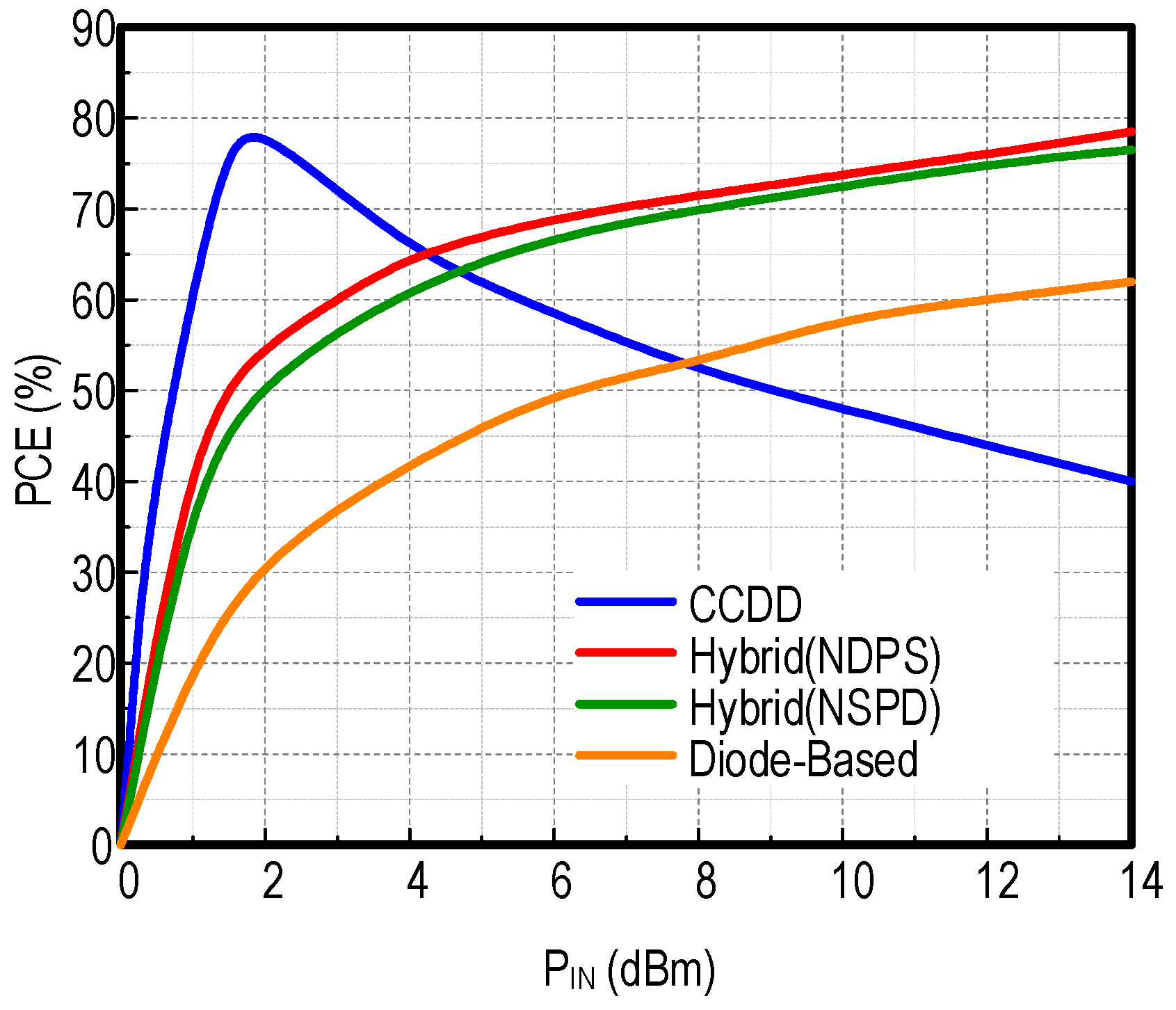
Figure 1a shows the CCDD rectifier. The rectifier receives differential signals and accumulates a common-mode gate voltage to bias the MOSFETs. It reduces the threshold voltage of the MOSFETs. The CCDD rectifier operates better in subthreshold [16] and threshold regions than other rectifier topologies. Therefore, the CCDD rectifier achieves peak PCE at a low input power level. On the contrary, at high input power, the CCDD rectifier suffers from reverse leakage due to the bidirectionality of the CMOS devices [14]. The subsequent rectifier topology is a diode-based configuration. Figure 1b shows the four diode-connected MOSFETs to rectify the differential signals. Due to the threshold voltage of the two diode-connected transistors in each signal path, this topology has a high dropout voltage. In contrast with CCDD topology, the diode-based configuration achieves low PCE at a low input power due to the forward voltage drop at the diodes. However, this connection significantly prevents the reverse current flow, achieving high PCE at a high input power level. The other configuration is a hybrid switch-diode-based rectifier, as illustrated in Figure 1c,d. It consists of two MOSFETs in diode configuration and the other two in switch configuration. In one signal path, there is a diode and a switch. Therefore, the dropout voltage and reverse leakage are reduced compared to the diode and CCDD configurations, respectively. The hybrid configuration merges the pros of the diode connected and CCDD topology. Figure 2 depicts the performance of various rectifier topologies extracted from [13]. The figure shows that the CCDD rectifier achieves high PCE at a low input power and degrades drastically at a high input power. It is demonstrated that the hybrid configuration obtained higher PCE than the diode-based rectifier at all input power levels. At a low input power level, the CCDD performs better, whereas the hybrid surpasses CCDD at a high input power level.

2.2. Proposed Circuit Architecture

The aim of the proposed front-end RFEH is to obtain high PCE at a wide input power range to improve the practicality of an RFEH system. By employing standard CMOS, different configurations can be achieved by altering the transistors’ gate connection. Based on the analysis in Section 2.1, a combination of CCDD and a hybrid topology would provide a wide PDR, as illustrated in Figure 3. The proposed front-end RFEH system consists of an IMN to achieve maximum power transfer and reduce power reflection, the main rectifier for scavenging the RF to DC, an auxiliary rectifier for a constant comparison of output voltage, and a control logic circuit as the adaptive switching control. Figure 4a,b illustrate the rectifier configuration during low input RF power and high RF input power, respectively, where the top architecture block diagram of the front-end is described in Figure 5.

3. Circuit Description

3.1. Main Rectifier

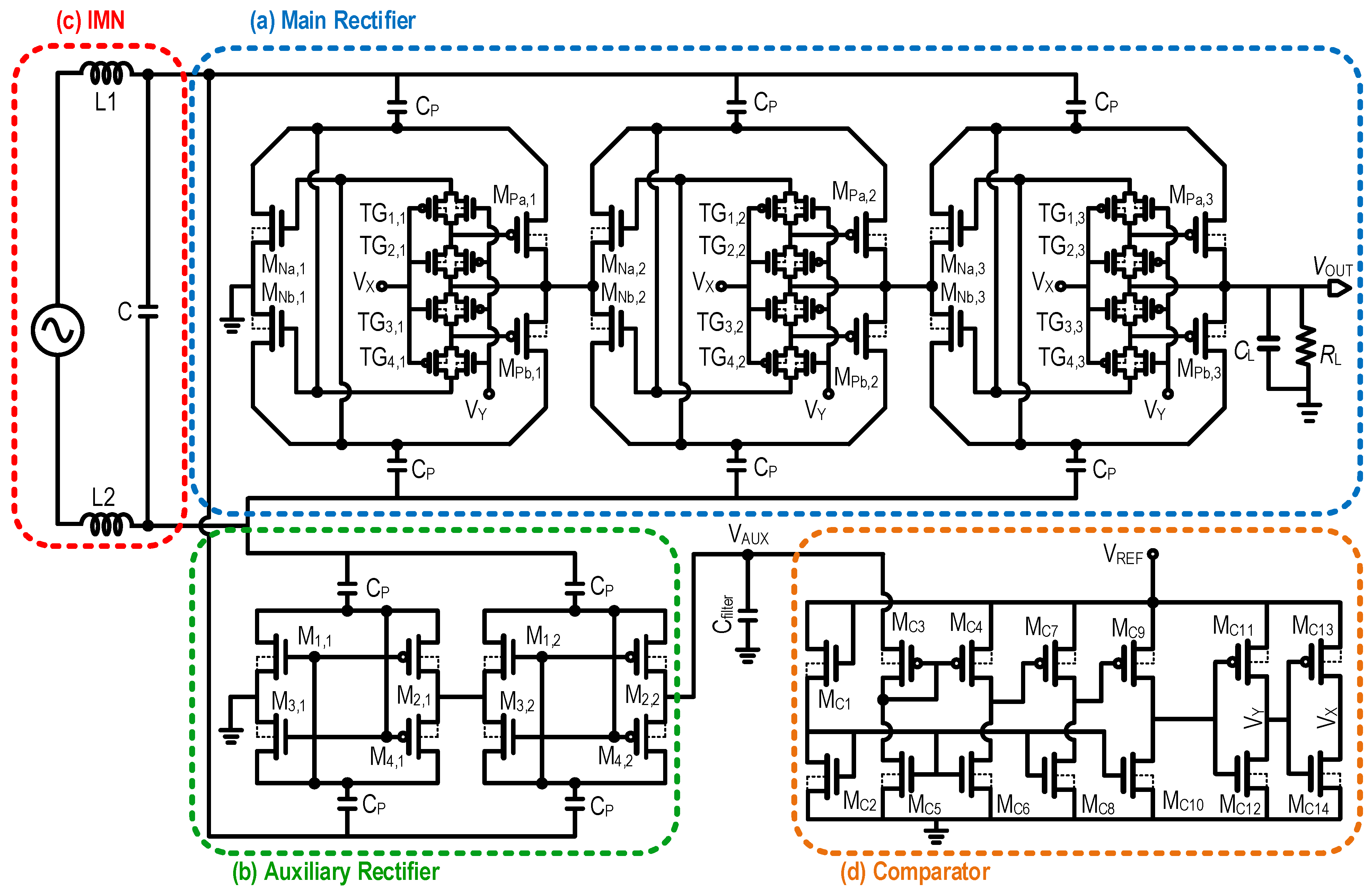
Figure 5a depicts the main rectifier circuit. It has three cascade stages of reconfigurable CCDD topology rectifiers. In each stage, there are four transmission gates (TG1-TG4). The transmission gates are controlled by the control logic circuit. To increase the sensitivity of the rectifier, a low-threshold-voltage transistor is used. The two rectifying NMOS have W/L of 30 while the PMOS has W/L of 60, because the hole mobility of PMOS is two times smaller than the electron mobility of NMOS. For State 1, where the input power is low, TG1 and TG2 are switched on, while TG3 and TG4 are off. It forms a conventional CCDD. For State 2, where the input power is high, TG3 and TG4 are on, and TG1 and TG2 are off. With this configuration, the PMOS is in a diode-connected state, and NMOS is in a switch configuration. It forms a hybrid rectifier topology similar to Figure 1d. PMOS is connected directly to the output, so the reverse current is higher. Therefore, the diode connections are designed at PMOS. The two switches in the hybrid topology contribute to high forward conduction at high input power, and the two diodes are in a reverse-bias state to control the high current flow from the output.
Unlike a full diode topology in [11], where the forward conduction is suppressed by the diodes, the proposed scheme balances forward conduction and controls reverse leakage. In contrast with [8,9], the proposed rectifier will not reduce forward conduction at low input power as it is a conventional CCDD rectifier. At the same time, the peak PCE occurs at low input power, which is favorable for far-field ambient energy harvesting.

3.2. Auxiliary Rectifier

As the proposed hybrid rectifier will be reconfigured into different topologies at different input power, it is necessary to detect the input power level to determine the switching point for the rectifier’s topology reconfiguration. The idea is to compare a target voltage signal which represents the input power level with the switching point voltage. If the target voltage is lower than the switching point voltage, the input power is considered low, and the circuit will be reconfigured into CCDD topology. Similarly, if the target voltage is greater than the switching point voltage, the circuit will be reconfigured into switch-diode-based topology.
The input voltage (RF+ and RF−) is not suitable to be used as the target signal, which represents the input power level, due to the large fluctuation in the AC voltage. The main rectifier’s DC output is also unsuitable as the target signal because its output voltage varies in different topologies.
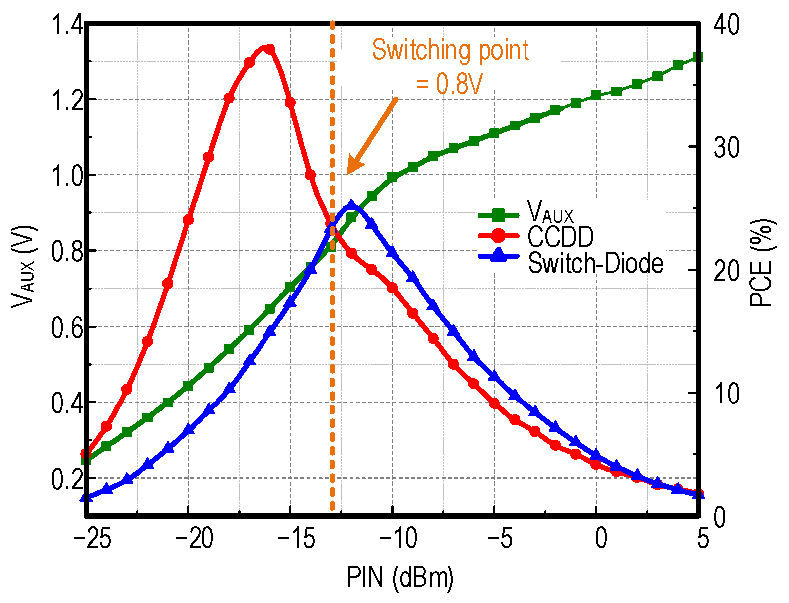
An auxiliary rectifier is used in this work to furnish a stable voltage to determine the rectifier’s switching point. The auxiliary rectifier offers an independent output voltage from the main rectifier. In other words, the output voltage of the auxiliary rectifier (VAUX) will not be affected by the change in the main rectifier’s topology; hence, it is ideally used in triggering the topology switching. A conventional three-stage CCDD is implemented as the auxiliary rectifier in this work, offering an independent DC voltage representing the input power level. As shown in Figure 6, the VAUX portrays a linear relationship with the increment in the PIN. The performance of the CCDD topology is better when VAUX is lower than 800 mV, while the performance of the diode-based topology is better when VAUX rises beyond 800 mV. Based on this relationship, we can assign VAUX = 800 mV as the rectifier’s topology reconfiguration switching point.

3.3. Impedance Matching Network

In front-end RFEH, the signal scavenged directly from the antenna to the rectifier results in high reflection and power loss. Thus, an IMN is essential to reduce power reflection and provide passive amplification. In a perfect match condition, the antenna’s resistance equals to rectifier’s equivalent resistance, while the reactance of the antenna and rectifier is in the conjugate. The matched impedance condition only occurs at the resonance frequency, as the reactance is a frequency-dependent parameter. At the resonance frequency, maximum power transfer occurs. As the frequency deviates further from the resonance frequency, the matching is progressively poor, along with increased power reflection. The performance of the matching is evaluated by the reflection coefficient, S11, of the circuit. The lower the S11, the better the matching. To realize the matching, the impedance of the rectifier is first simulated. The rectifier can be modeled as a series or parallel resistor and capacitor set [17].
In most cases, the simulated impedance is in series form, but it is transformable as long as the circuit maintains the same quality factor, Q. Figure 7 demonstrates the conversion of the rectifier model from series or parallel or vice versa. The conversion can be performed by referring to Equations (1)–(5), where QS and QP are the Q of the rectifier model in series and parallel, respectively.
Q S = Q P = Q
Q S = 1 ω C S R S
Q P = ω C P R P
R P = R S ( 1 + Q 2 )
C P = C S 1 + 1 Q 2
There are four configurations of a conventional L-network [18], as shown in Figure 8. It is categorized into two categories, with either the real impedance of the source, RS being larger or smaller than the rectifier’s equivalent series real impedance, RL. Each category has a high or low pass to block or pass the DC signal. A shunt capacitor and series inductor pass DC. On the contrary, a series capacitor and shunt inductor pass DC. In most cases, a series capacitor is used to prevent the backflow of signal from the rectifier to the source. However, since the proposed system has a diode configuration, it is sufficient to block the high reverse current. Therefore, the IMN design is focused on matching the rectifier and antenna impedances only.
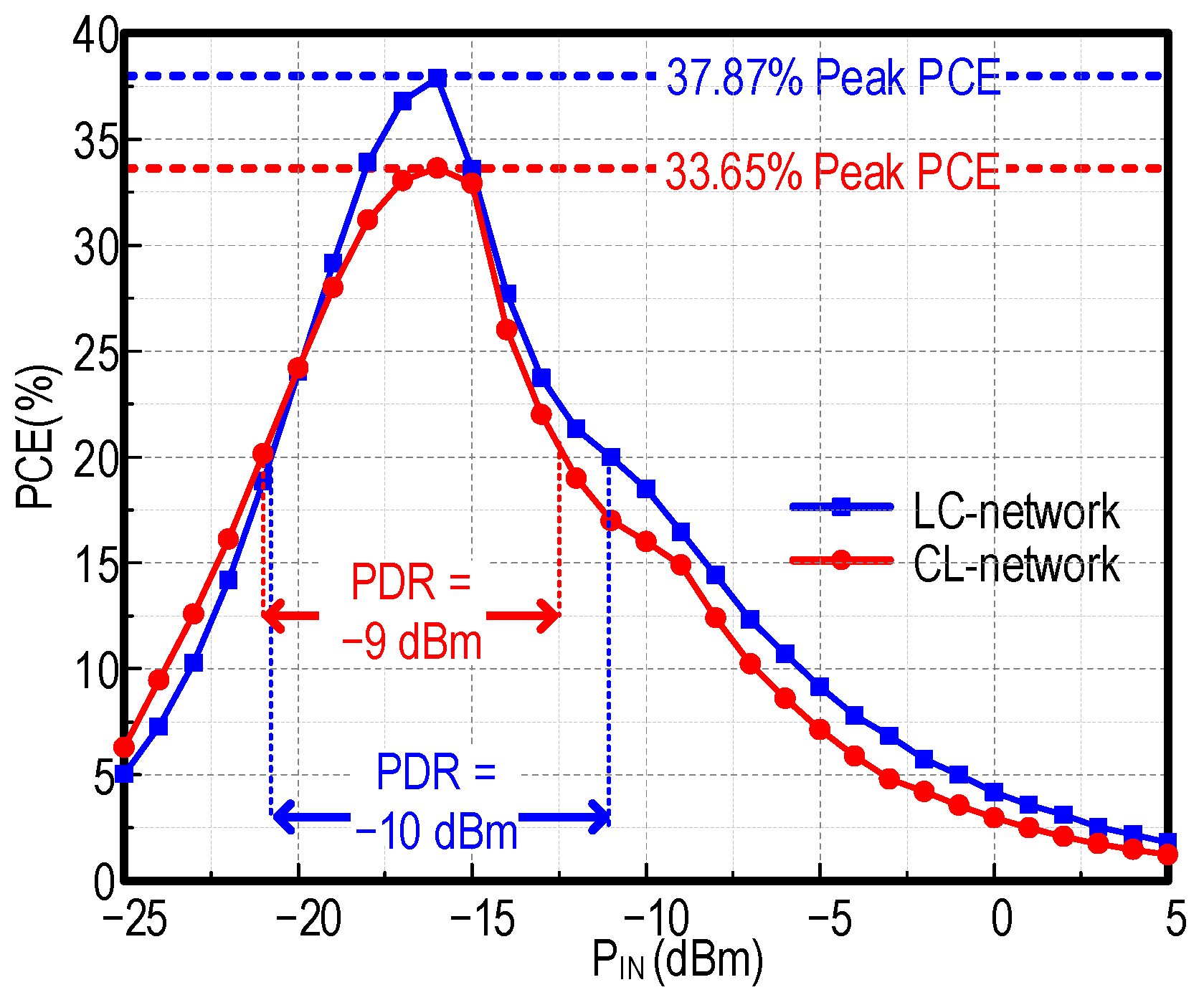
The simulation of the rectifier’s impedance shows that the real impedance is much larger than the antenna’s (standard 50 Ω). Consequently, the L-network that matches the condition will be Figure 8c or Figure 8d. For a fair comparison, the rectifier sizing, load, capacitance, inductor sizing, and Q are fixed. Figure 9 shows the result of PCE for the RFEH front-end when CL and LC networks are employed with the proposed rectifier. At the matching frequency, 900 MHz, the L-C network has a higher peak and overall PCE than the C-L network. Therefore, the IMN in Figure 8c is selected for the matching.
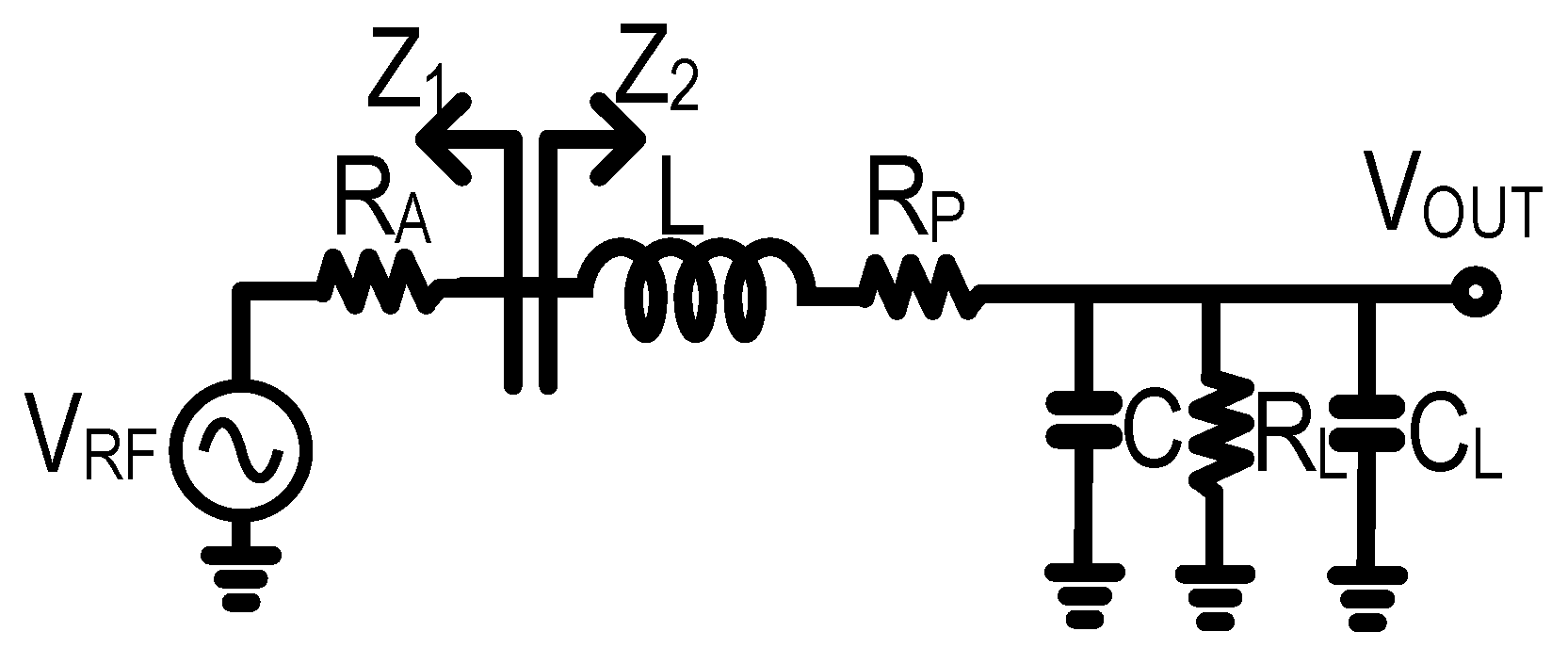
In this work, an on-chip L network was used by cascading four inductors in series to increase the inductance while maintaining a high-quality factor. It was tuned to match at 900 MHz, between a 50 Ω antenna and the proposed reconfigurable rectifier with the auxiliary rectifier. Considering that the Q of the inductor affects the matching parameter, the following equations were deduced to obtain matching. A resistor was placed in series with the inductor to represent the parasitic of the inductor. From (8) and (10), the parameter of matching components can be calculated based on the desired harvesting frequency. The matching capacitor is assumed to be ideal. Figure 10 exemplifies the model for the matching condition, where RL and CL are the equivalent impedance of the proposed rectifier and auxiliary rectifier, RA is the antenna resistance, L and C are the matching network’s passive components, and RP represents the parasitic of the matching inductor. The auxiliary rectifier, integrated in parallel with the main rectifier, reduced the equivalent impedance of the rectifiers (RL and CL) to be matched, hence reducing the required matching transformation [19]. To match, Re(Z1) = Re(Z2), and Img(Z1) = *Img(Z2).
Z 2 = j ω L + R P + ( 1 j ω C | | R L | | 1 j ω C L )
Z 2 = j ω L + R P + 1 R L j ω ( C + C L ) ( 1 R L ) 2 + [ ω ( C + C L ) ] 2
R e [ Z 2 ] = R A = R P + R L 1 + [ R L ω ( C + C L ) ] 2
I m g [ Z 2 ] = 0 = ω L ω R L 2 ( C + C L ) 1 + [ R L ω ( C + C L ) ] 2
ω L = ω R L 2 ( C + C L ) 1 + [ R L ω ( C + C L ) ] 2
k = R L R P + R L 1 + [ R L ω ( C + C L ) ] 2
A = 1 2 R L R A = 1 2 k
Based on the equations above, the transformation ratio, known as k = RL/RA [20] can be found in (11). The equation shows that RP plays an important role in the transformation performance. The Q of the inductor when parasitic assumed in series is ω L R P . When the rectifier parameters are fixed, the increase in RP will decrease k. It shows that the parasitic resistance will directly affect the transformation ratio. Furthermore, the matching network contributes to the passive amplification to provide higher sensitivity of the system. In [21], the passive amplification is defined as (12). The higher the k, the larger the amplification. Therefore, it is concluded that the parasitic of the inductor plays a big part in the impedance matching. The higher the Q, the lower the RP, the better the performance of the matching network.
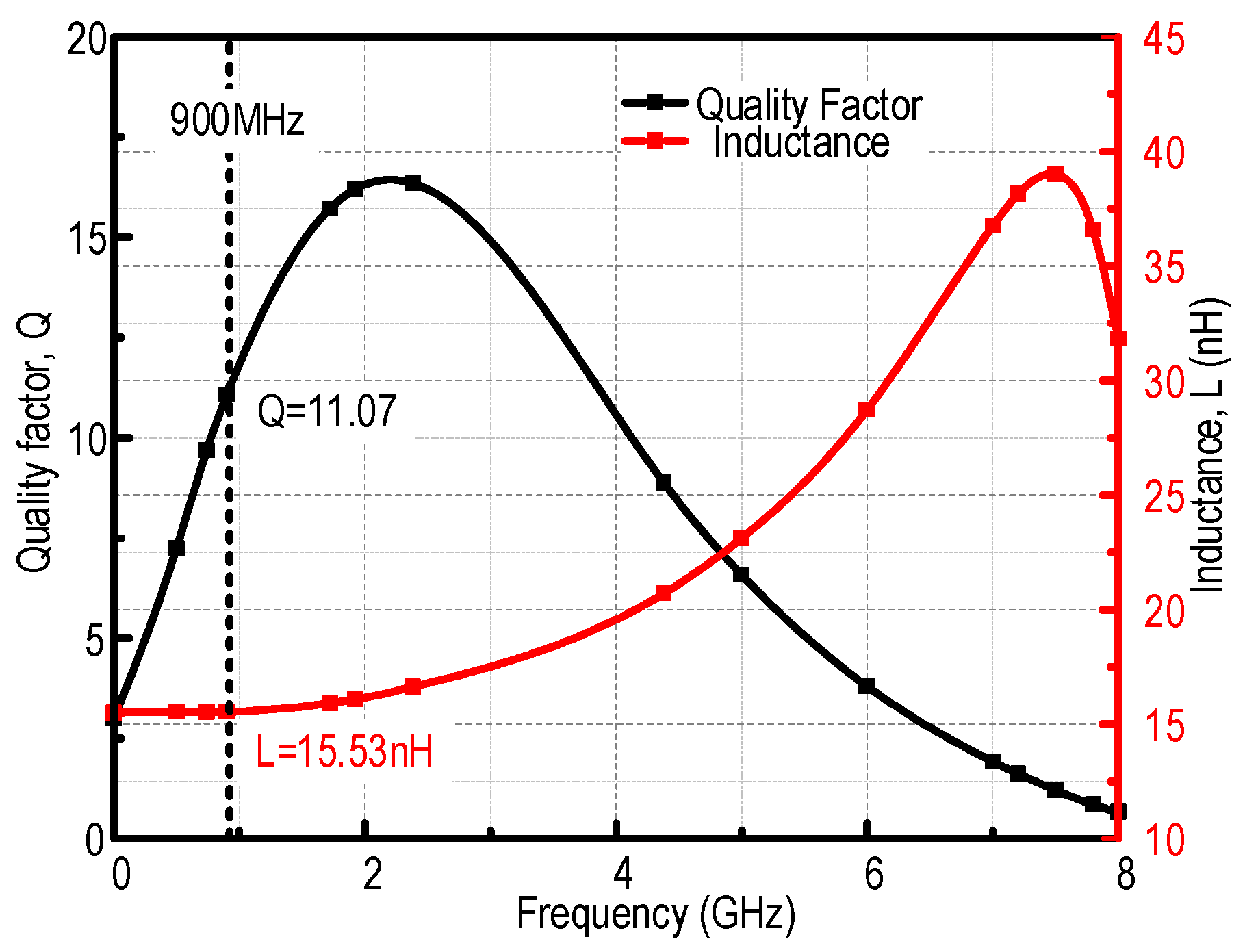
To maintain a high-quality factor at high total inductance, four similar inductors are cascaded to increase the total inductance while maintaining high quality factor at 900 MHz. The parameters of the inductor are shown in Figure 11. The parasitics are included and the parameters are simulated using Sonnet EM Simulator. At 900 MHz, it has a Q of 11.07, and inductance of 15.53 nH. Upon stacking four similar inductors in series, the total inductance is 62.12 nH.

3.4. Control Logic Circuit

The proposed work adopted a CMOS Op-Amp comparator from [22] to determine the rectifier’s topology configuration. As depicted in Figure 5d, the comparator consists of a source input stage for voltage comparison, an output stage that provides the output signal, and a biasing stage responsible for supplying a bias voltage to the source input and the output stage. At the source-input stage, the comparator accounts for an external reference voltage (VREF) of 800 mV to be compared with the auxiliary rectifier’s output voltage (VAUX). The external VREF serves as a reference for the switching point to validate the input power level to be either high or low. In the scenario where VAUX is lower than the VREF (VAUX < 800 mV), the input power is considered low, whereas when VAUX is higher than the VREF (VAUX > 800 mV), the PIN is considered high. A stable reference source is required; therefore, an independent external voltage source is supplied. The output stage compromises two CMOS-connected inverters in generating the control signals VX and VY to configure the rectifier into a different topology.
Figure 6 portrays the VAUX at different input powers. At a low input power, as VREF is higher than VAUX (VAUX < 800 mV), the comparator will yield an output with a logic low. This will activate State 1, where TG1 and TG2 are switched on while TG3 and TG4 are off, configuring the rectifier into conventional CCDD topology. At a high input power, VAUX rises above 800 mV. The comparator will yield a logic-high output as VREF is now lower than the VAUX. At this state, the rectifier will be configured into a diode-based topology with TG1, TG2 deactivated and TG3 and TG4 activated.

4. Postlayout and Simulation Results

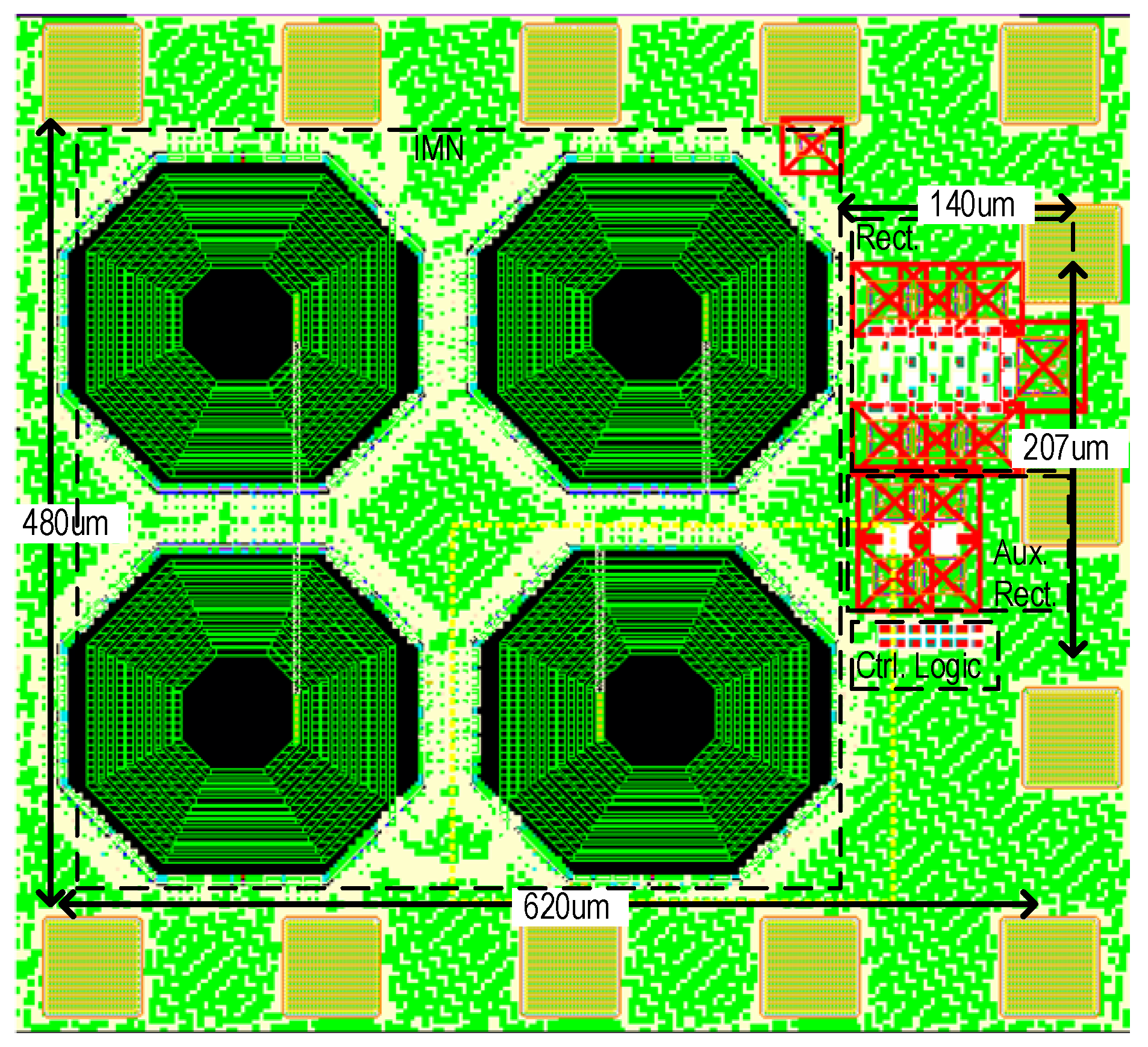
The proposed rectifier and an on-chip LC network are implemented in a 65 nm CMOS process, as shown in Figure 12. Four inductors are connected in series to form high inductance while maintaining high Q for matching. The other blocks, such as the rectifier, auxiliary rectifier, and control logic, are highlighted in the figure. Low-voltage-threshold (LVT) transistors are used for the main and auxiliary rectifiers to reduce forward conduction loss and normal transistors are used for the control logic unit. MIM capacitor is used throughout the entire design. Table 1 records the design’s components value. The total size of the design, excluding the bond pads, is 620 µm × 480 µm.
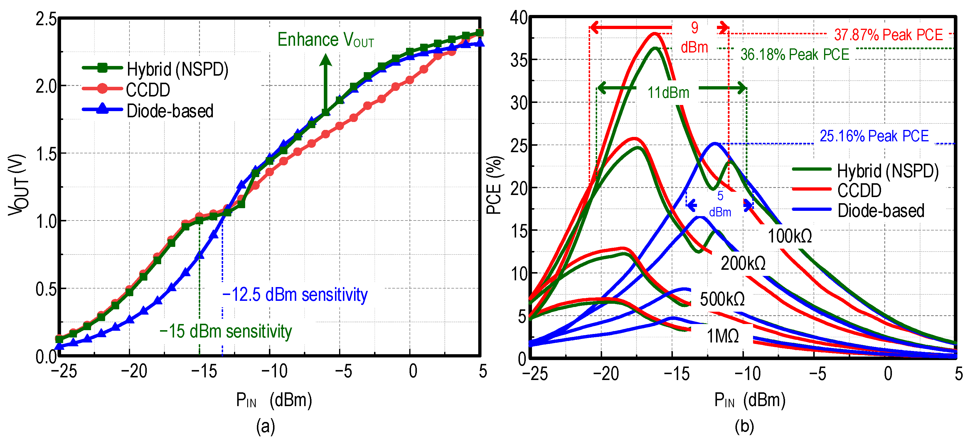
The performance of the rectifier block was investigated independently. Figure 13 depicts the output voltage across a wide range of input power for the CCDD topology, diode-based topology, and the proposed hybrid topology with switch controls. The CCDD topology obtains higher output voltage at low input power, whereas the diode-based topology has a higher output at high input harvesting power. The proposed rectifier’s performance is exhibited in a combination of both, with a slight voltage drop at high input. This is due to the transmission gates, as there is some reverse leakage through the TG1 and TG2 during the diode-based configuration, where the switches are not fully turned off. Although the leakage is present, the proposed rectifier scheme provides a wider PDR due to its hybrid configuration. Contrary to the PCE significantly degrading at high input power, the PCE increase at the all-load condition at high input power compared to the conventional CCDD rectifier. It shows that the control logic circuit functions to switch at the exact condition.
The on-chip LC-network IMN is implemented along with the proposed rectifier. The output voltage and PCE of the front-end RFEH system are presented in Figure 14a,b, respectively. The switching point occurs at approximately −12 dBm. The PCE graph shows a drop in the PCE at the switching point. Subsequently, it is increased after the configuration is changed to a hybrid switch-diode-based configuration. Due to the switching losses and transition, there is a dip in the PCE graph. However, once the switches are fully turned on, the proposed hybrid configuration follows the PCE of the diode-based configuration at high input power.
The PCE of the rectifier is calculated by incorporating the power reflection, denoted by (12), while the front-end RFEH is calculated by (13). The power reflection is not included in (13) as a matching network is adopted; hence, it achieves maximum power transfer at the desired frequency. Figure 15 illustrates the post-layout result on the reflection coefficient, S11, of the proposed front-end RFEH. It is matched at 900 MHz with an S11 of −14 dB. POUT refers to the output power of the rectifier, with VOUT2/RL, PSIG is the input signal excluding the power reflection, and |S11|is the power reflection. The rectifier achieves a peak PCE of 88.7% at −22 dBm, while the fully integrated RFEH front-end obtains a peak PCE of 36%.
P C E R E C   ( % ) = P O U T P SIG ( 1 | S 11 | 2 ) × 100 %  
P C E R F E H   ( % ) = P O U T P SIG × 100 %  
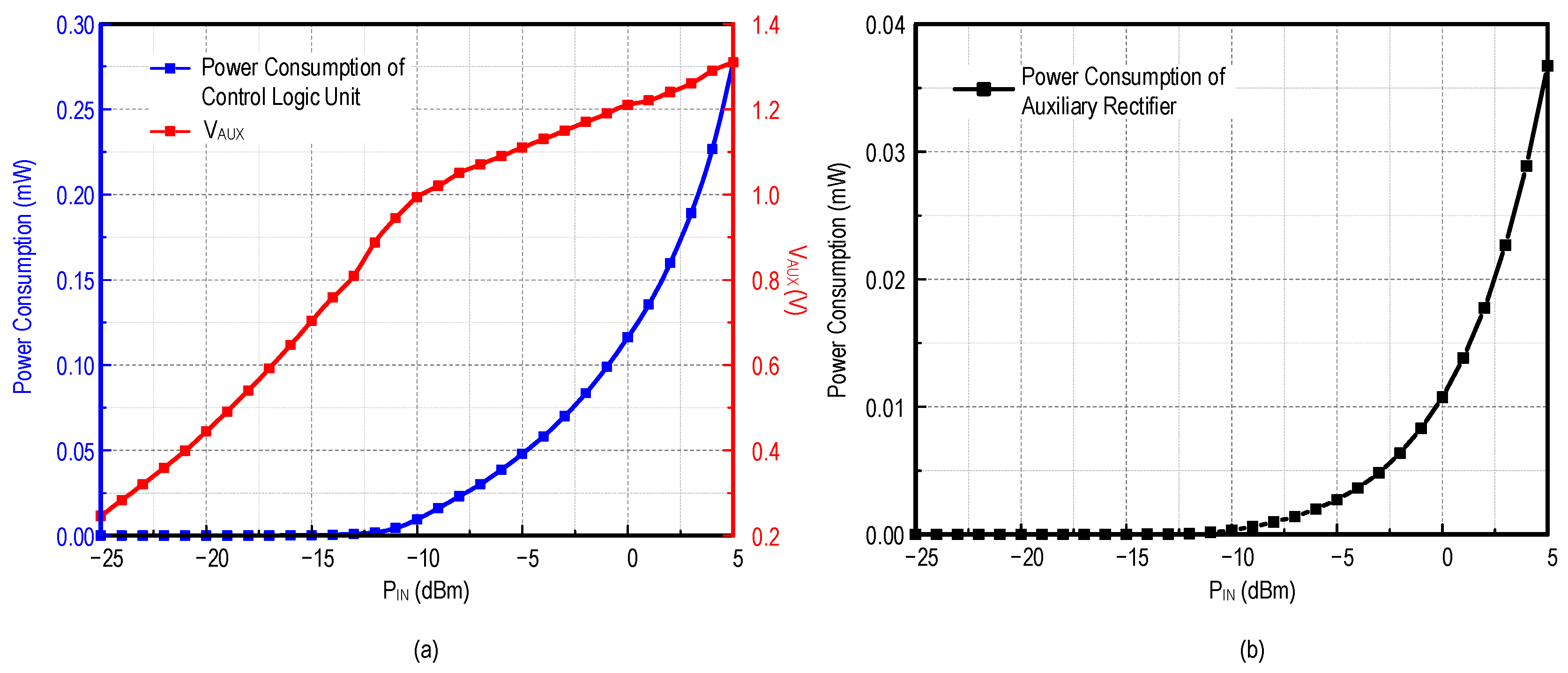
Figure 16a depicted the relationship of PIN, VAUX, and the power consumption of the control logic unit. VAUX increases linearly with the increment in PIN due to the boosting effect of the two-stage auxiliary rectifier. The power consumption of the control logic unit increases exponentially with the increment in PIN. This is because VAUX, which is the source of the control logic unit, is increased, causing more power to flow into the control logic unit. The power consumption of the control logic unit is negligible as PIN is lower than −10 dBm and its power consumption increases with the PIN and reaches a peak consumption of 0.278 mW at 5 dBm. Figure 16b shows the power consumption of the auxiliary rectifier. It shows a similar behavior where the power consumption is negligible when PIN is below −10 dBm and it increases exponentially until a peak consumption of 0.037 mW at 5 dBm.
The scope of this proposed work was to extend the PDR of the rectifier. The PDR is defined as the input power range where the rectifier’s PCE upholds above 20% [9]. At 100 KΩ, the CCDD and diode-based rectifier has a PDR of only 20 dB and 16 dB, respectively. In implementing the proposed hybrid configuration by switching the PMOS connections, the rectifier achieves a PDR of 23 dB. To test the robustness of the proposed front-end RFEH, simulation of the proposed rectifier with respect to process corner and temperate were performed. The switching point, sensitivity, and peak PCE of the proposed front-end RFEH at typical-typical, slow-slow, and fast-fast processes at different temperature conditions are shown in Figure 17. Generally, the peak PCE is higher at −40 °C and it is at lowest for the fast-fast process. However, the peak PCE after process and temperature variation remains a minimum of 23% with matching network included. It is reasonable for fully integrated applications. Figure 17a proves the practicality of the proposed circuit as the switching point for the hybrid configuration only varies for less than 200 mV at different processes and temperatures. For sensitivity with IMN included, it remains the same for all the processes at −40 °C and reduces gradually with the increase in temperature. There is only a difference of 4 dBm between the worst and highest sensitivity. The process and temperature variation have shown the robustness of the proposed front-end RFEH at different conditions.
Table 2 summarizes the performance comparison with state-of-the-art RFEH rectifiers. The proposed reconfigurable rectifier with extended PDR incorporates the CCDD rectifier at low input and switches to a hybrid-based switch-diode configuration at high input. A comparison is drawn by assessing the rectifier block and by incorporating the computation of power reflection. Hence, the result for the RFEH front-end with IMN block is not included. This work has comparable sensitivity with other state-of-the-art architectures and achieves a sensitivity of −21 dBm. Based on Table 2, it is shown that the CCDD topology achieves a higher peak PCE than the diode-based Dickson topology. The proposed rectifier surpasses the performance of other research in peak PCE evaluation. Despite reporting better sensitivity, the results of [2,10] achieve unfavorable peak PCE and PDR performance. For [12], a similar concept of configuring between switch and switch-diode configurations was applied; however, only manual switching and conceptual results were shown. [12] compared the four rectifier topologies shown in Figure 1 and have shown the results for the four topologies. There were no results with hybrid rectifier configuration.

5. Conclusions

A novel wide-dynamic-range hybrid reconfigurable rectifier for an RF energy harvesting system is proposed in this work, which can be reconfigured into different topologies based on the input voltage to enhance the rectifier’s PCE and sensitivity. At low input power, the hybrid rectifier is configured into a CCDD topology that benefits from the low conduction loss advantage due to the cross-coupled transistor pairs. At higher input power, the rectifier is reconfigured into a hybrid diode-based (NSPD) topology to reduce the reverse current leakage. Designed in 65 nm CMOS technology, the proposed rectifier achieves a peak PCE of 88.7% at 100 KΩ, surpassing the performance of all existing research. In addition, the reconfigurable hybrid design offers a wide PDR of 16 dB for PCE over 40%. It attains superior sensitivity of −21 dBm to achieve 1 V with a 1 MΩ load condition.

Author Contributions

Conceptualization, W.X.L., J.K.Y., G.C. and K.K.P.C.; methodology, W.X.L. and J.K.Y.; software, W.X.L. and J.K.Y.; data curation, W.X.L., J.K.Y. and G.C.; writing—original draft preparation, W.X.L. and J.K.Y.; writing—review and editing, W.X.L., J.K.Y., G.C., H.R. and K.K.P.C.; investigation, W.X.L., J.K.Y. and G.C.; supervision, H.R., Y.C., P.-I.M. and R.P.M.; validation, W.X.L. and J.K.Y.; funding acquisition, H.R. All authors have read and agreed to the published version of the manuscript.

Funding

This work was supported by the Collaborative Research in Engineering, Science and Technology Center (CREST) Program under Grant T05C2-19(PV026-2020).

Institutional Review Board Statement

Not applicable.

Informed Consent Statement

Not applicable.

Data Availability Statement

Data are contained within the article.

Conflicts of Interest

The authors declare no conflict of interest.

References

  1. Luo, Y.; Pu, L.; Wang, G.; Zhao, Y. RF Energy Harvesting Wireless Communications: RF Environment, Device Hardware and Practical Issues. Sensors 2019, 19, 3010. [Google Scholar] [CrossRef] [PubMed] [Green Version]
  2. Ho, T.S.; Ramiah, H.; Churchill, K.K.P.; Chen, Y.; Lim, C.C.; Lai, N.S.; Mak, P.-I.; Martins, R.P. Low Voltage Switched-Capacitive-Based Reconfigurable Charge Pumps for Energy Harvesting Systems: An Overview. IEEE Access 2022, 10, 126910–126930. [Google Scholar] [CrossRef]
  3. Saffari, P.; Basaligheh, A.; Moez, K. An RF-to-DC Rectifier With High Efficiency Over Wide Input Power Range for RF Energy Harvesting Applications. IEEE Trans. Circuits Syst. I Regul. Pap. 2019, 66, 4862–4875. [Google Scholar] [CrossRef]
  4. Basim, M.; Khan, D.; Ain, Q.U.; Shehzad, K.; Shah, S.A.A.; Jang, B.-G.; Pu, Y.-G.; Yoo, J.-M.; Kim, J.-T.; Lee, K.-Y. A Highly Efficient RF-DC Converter for Energy Harvesting Applications Using a Threshold Voltage Cancellation Scheme. Sensors 2022, 22, 2659. [Google Scholar] [CrossRef]
  5. Chong, G.; Ramiah, H.; Yin, J.; Rajendran, J.; Mak, P.I.; Martins, R.P. A Wide-PCE-Dynamic-Range CMOS Cross-Coupled Differential-Drive Rectifier for Ambient RF Energy Harvesting. IEEE Trans. Circuits Syst. II Express Briefs 2021, 68, 1743–1747. [Google Scholar] [CrossRef]
  6. Churchill, K.K.P.; Chong, G.; Ramiah, H.; Ahmad, M.; Rajendran, J. Low-Voltage Capacitive-Based Step-Up DC-DC Converters for RF Energy Harvesting System: A Review. IEEE Access 2020, 8, 186393–186407. [Google Scholar] [CrossRef]
  7. Yong, J.K.; Ramiah, H.; Churchill, K.K.P.; Chong, G.; Mekhilef, S.; Chen, Y.; Mak, P.-I.; Martins, R.P. A 0.1-V VIN Subthreshold 3-Stage Dual-Branch Charge Pump With 43.4% Peak Power Conversion Efficiency Using Advanced Dynamic Gate-Bias. IEEE Trans. Circuits Syst. II Express Briefs 2022, 9, 3929–3933. [Google Scholar] [CrossRef]
  8. Almansouri, A.S.; Ouda, M.; Salama, K.N. A CMOS RF-to-DC Power Converter With 86% Efficiency and −19.2-dBm Sensitivity. IEEE Trans. Microw. Theory Tech. 2018, 66, 2409–2415. [Google Scholar] [CrossRef] [Green Version]
  9. Ouda, M.H.; Khalil, W.; Salama, K.N. Self-Biased Differential Rectifier with Enhanced Dynamic Range for Wireless Powering. IEEE Trans. Circuits Syst. II Express Briefs 2017, 64, 515–519. [Google Scholar] [CrossRef] [Green Version]
  10. Lu, Y.; Dai, H.; Huang, M.; Law, M.-K.; Sin, S.-W.; Seng-Pan, U.; Martins, R.P. A Wide Input Range Dual-Path CMOS Rectifier for RF Energy Harvesting. IEEE Trans. Circuits Syst. II Express Briefs 2017, 64, 166–170. [Google Scholar] [CrossRef]
  11. Choo, A.; Ramiah, H.; Churchill, K.K.P.; Chen, Y.; Mekhilef, S.; Mak, P.-I.; Martins, R.P. A Reconfigurable CMOS Rectifier With 14-dB Power Dynamic Range Achieving >36-dB/mm2 FoM for RF-Based Hybrid Energy Harvesting. IEEE Trans. Very Large Scale Integr. (VLSI) Syst. 2022, 30, 1533–1537. [Google Scholar] [CrossRef]
  12. Heo, B.-R.; Kwon, I. A Dual-Band Wide-Input-Range Adaptive CMOS RF–DC Converter for Ambient RF Energy Harvesting. Sensors 2021, 21, 7483. [Google Scholar] [CrossRef] [PubMed]
  13. Guler, U.; Jia, Y.; Ghovanloo, M. A Reconfigurable Passive RF-to-DC Converter for Wireless IoT Applications. IEEE Trans. Circuits Syst. II Express Briefs 2019, 66, 1800–1804. [Google Scholar] [CrossRef]
  14. Ouda, M.H.; Khalil, W.; Salama, K.N. Wide-Range Adaptive RF-to-DC Power Converter for UHF RFIDs. IEEE Microw. Wirel. Compon. Lett. 2016, 26, 634–636. [Google Scholar] [CrossRef] [Green Version]
  15. Alhoshany, A. A 900 MHz, Wide-Input Range, High-Efficiency, Differential CMOS Rectifier for Ambient Wireless Powering. Sensors 2022, 22, 974. [Google Scholar] [CrossRef]
  16. Chong, G.C.; Ramiah, H.; Yin, J.; Rajendran, J.; Wong, W.R.; Mak, P.-I.; Martins, R.P.; Ru, W.W. CMOS Cross-Coupled Differential-Drive Rectifier in Subthreshold Operation for Ambient RF Energy Harvesting—Model and Analysis. IEEE Trans. Circuits Syst. II Express Briefs 2019, 66, 1942–1946. [Google Scholar] [CrossRef]
  17. Lian, W.X.; Ramiah, H.; Chong, G.; Churchill, K.K.P.; Lai, N.S.; Chen, Y.; Mak, P.-I.; Martins, R.P. A −20-dBm Sensitivity RF Energy-Harvesting Rectifier Front End Using a Transformer IMN. IEEE Trans. Very Large Scale Integr. (VLSI) Syst. 2022, 30, 1808–1812. [Google Scholar] [CrossRef]
  18. Chun, A.C.C.; Ramiah, H.; Mekhilef, S. Wide Power Dynamic Range CMOS RF-DC Rectifier for RF Energy Harvesting System: A Review. IEEE Access 2022, 10, 23948–23963. [Google Scholar] [CrossRef]
  19. Pakkirisami Churchill, K.K.; Ramiah, H.; Chong, G.; Chen, Y.; Mak, P.I.; Martins, R.P. A Fully-Integrated Ambient RF Energy Harvesting System with 423-μW Output Power. Sensors 2022, 22, 4415. [Google Scholar] [CrossRef]
  20. Soltani, N.; Yuan, F. A step-up transformer impedance transformation technique for efficient power harvesting of passive transponders. Microelectron. J. 2010, 41, 0026–2692. [Google Scholar] [CrossRef]
  21. Soltani, N.; Yuan, F. A High-Gain Power-Matching Technique for Efficient Radio-Frequency Power Harvest of Passive Wireless Microsystems. IEEE Trans. Circuits Syst. I Regul. Pap. 2010, 57, 2685–2695. [Google Scholar] [CrossRef]
  22. Yuen, P.W.; Chong, G.; Ramiah, H. A high efficient dual-output rectifier for piezoelectric energy harvesting. Int. J. Electron. Commun. 2019, 111, 1434–8411. [Google Scholar] [CrossRef]
  23. Moghaddam, A.K.; Chuah, J.; Ramiah, H.; Ahmadian, J.; Mak, P.I.; Martins, R.P. A 73.9%-Efficiency CMOS Rectifier Using a Lower DC Feeding (LDCF) Self-Body-Biasing Technique for Far-Field RF Energy-Harvesting Systems. IEEE Trans. Circuits Syst. I Regul. Pap. 2017, 64, 992–1002. [Google Scholar] [CrossRef]
Figure 1. The different configurations of a rectifier: (a) conventional CCDD, (b) diode-connected dual path rectifier, (c) hybrid topology (NDPS), (d) hybrid topology (NSPD).
Electronics 12 00175 g001
Figure 2. Simulated PCE of the four rectifier configurations [13].
Electronics 12 00175 g002
Figure 3. Conceptualization of the PCE curve on the proposed reconfigurable rectifier.
Electronics 12 00175 g003
Figure 4. Top architecture of the proposed front-end RFEH: (a) at low input power, (b) at a high input power.
Electronics 12 00175 g004
Figure 5. The schematic of the proposed reconfigurable hybrid rectifier with (a) main rectifier, (b) auxiliary rectifier, (c) impedance matching network (IMN), and (d) comparator.
Electronics 12 00175 g005
Figure 6. Relationship between input power, auxiliary charge pump voltage, and the switching point of the rectifier’s topology.
Electronics 12 00175 g006
Figure 7. Rectifier’s equivalent impedance model interchangeable from series to parallel.
Electronics 12 00175 g007
Figure 8. Four configurations of L-network: (a) Low pass CL for RS > RL, (b) High pass LC for RS > RL, (c) Low pass LC for RS < RL, (d) High pass CL for RS < RL.
Electronics 12 00175 g008
Figure 9. Comparison of LC and CL networks at 100 KΩ when rectifier parameters and the passive components sizing are fixed.
Electronics 12 00175 g009
Figure 10. Model of the matching condition for the RFEH front-end.
Electronics 12 00175 g010
Figure 11. Quality factor and inductance of the matching inductor, L, over frequency.
Electronics 12 00175 g011
Figure 12. Chip layout of the proposed RFEH front end.
Electronics 12 00175 g012
Figure 13. Postlayout simulation of (a) rectifier output voltage across different input power at 100 kΩ without matching, (b) the power conversion efficiency of rectifiers across different input powers at various load conditions.
Electronics 12 00175 g013
Figure 14. Postlayout simulation of (a) RFEH front-end output voltage across different input powers at 100 kΩ with impedance matching, (b) the power conversion efficiency across different input powers at various load conditions with impedance matching.
Electronics 12 00175 g014
Figure 15. Postlayout simulation of S11.
Electronics 12 00175 g015
Figure 16. (a) The relationship between the input power, auxiliary rectifier’s output voltage, and the power consumption of the control logic unit. (b) The power consumption of the auxiliary rectifier.
Electronics 12 00175 g016
Figure 17. Process corners simulation of proposed front-end RFEH for RL = 100 KΩ: (a) auxiliary rectifier switching voltage (V), (b) sensitivity, (c) PCE.
Electronics 12 00175 g017
Table 1. The proposed circuit’s components sizing.
Circuit BlocksCircuitComponents TypeComponents NameSize
Main RectifierRectifierNMOS (LVT)MNa & MNb18 μm
PMOS (LVT)PNa & PNb36 μm
MIM CapacitorCP1 pF
Transmission GateNMOS (LVT)TG (NMOS)2 μm
PMOS (LVT)TG (PMOS)4 μm
Auxiliary RectifierRectifierNMOS (LVT)M1 & M3600 nm
PMOS (LVT)M2 & M436 μm
MIM CapacitorCP1 pF
MIM CapacitorCFilter1 pF
Control Logic UnitComparatorNMOS (Standard)MC1,2,5,6,8,10,12,1421.6 μm
PMOS (Standard)MC3,4,7,9,11,137.2 u
Table 2. Performance benchmark with related State-of-the-art RFEH rectifiers.
ReferenceThis Work[3][5][8][10][11][23][13]
CMOS
Tech.
(nm)
6513013018065130130350
Frequency
(MHz)
9008969009009009009531356
Rectifier
Topology
CCDDDicksonCCDDCCDDCCDDDicksonCCDDCCDD
Proposed TechniqueReconfigurable hybrid switch-diode configurationVoltage CompensationSelf-body-biasingDouble-Sided Self-BiasingDual-PathReconfigurable No. of Stage/Series/
Parallel
Self-body-biasing/low-feeding DCManual hybrid switch-diode configuration
Sensitivity @1 V−21 dBm @1 MΩ−22 dBm @1 MΩ−18.7 dBm @100 KΩ−18.2 dBm @100 KΩ−17.7 dBm
@∞
−21.7 dBm @1 MΩ−6.5 dBm
@50 KΩ
3.22 dBm **
@500 KΩ
Rectifier’s Peak PCE88.7%
@100 KΩ
51%
@300 KΩ
80.3% @100 KΩ66%
@100 KΩ
36.5% @147 KΩ34.93%
@1 MΩ
69.5%
@2 KΩ
82% **
@500 KΩ
PDR (Rectifier PCE > 20%)23 dB10.5 dB17.5 dB *20 dB *11 dB14 dB13 dB *N.A.
PDR (Rectifier PCE > 40%)16 dB4 dB14.5 dB10.5 dBN.A.N.A.10 dBN.A.
PDR (Rectifier PCE > 60%)10 dBN.A.9 dB3 dBN.A.N.A.5 dBN.A.
Rectifier’s Effective Chip Area (mm2)0.0280.0530.0620.00880.0480.0390.0290.019
* Estimated from a graph. ** work does not include reconfiguration, estimated from combination of two different topologies
Disclaimer/Publisher’s Note: The statements, opinions and data contained in all publications are solely those of the individual author(s) and contributor(s) and not of MDPI and/or the editor(s). MDPI and/or the editor(s) disclaim responsibility for any injury to people or property resulting from any ideas, methods, instructions or products referred to in the content.