1. Introduction
Machine learning (ML) models, such as convolutional neural networks (CNNs) and deep neural networks (DNNs), are widely used in real-world applications. However, neural network structures have also increased in size, causing a bottleneck in the Von Neumann accelerator architecture. More specifically, the CPU must retrieve data from memory before processing it and then transfer it back to memory at the end of the computation in a Von Neumann architecture. This leads to additional energy consumption during data transfer, which reduces the energy efficiency of computing devices [
1]. Furthermore, limited memory bandwidth, high memory access latency, and long memory access paths limit inference speeds and cause substantial power consumption regardless of the performance of the logic circuit. However, in-memory computing can effectively overcome the bottlenecks in the Von Neumann architecture. The CIM architecture can achieve low memory access latency, parallel operation, and ultra-low power consumption, and close access to the arithmetic logic unit of the CIM architecture can overcome the bottlenecks of the Von Neumann architecture [
2].
The error rate of visual recognition by CNNs declined from 28% in 2010 to 3% in 2016 to become better than the 5% error rate in manual (i.e., human) visual recognition [
3]. CNNs have been integrated into embedded systems to solve image classification and pattern recognition problems. However, large CNNs may have millions of parameters and require up to tens of billions of operations to process an image frame [
4]. Therefore, accelerating the convolution operation yields the greatest improvement in performance. Iterative processing of the CNN layers is a common design feature of CNN accelerators. However, the intermediate data are too large to fit on the chip’s cache, and accelerator designs must, thus, use off-chip memory to store intermediate data between layers after processing. Due to the computational requirements of Internet of Things (IoT) and artificial intelligence (AI) applications, the cost of moving data between the central processing unit (CPU) and memory is a key limiter of performance.
CPU and GPU performance growth is approximately 60% per year; however, the performance increases in memory reach only up to 7% each year [
5]. The data transfer rate in memory is insufficiently fast for the computational speed of the CPU; thus, the CPU is typically “data hungry”. Although deep learning processor performance has grown exponentially, most power consumption occurs during the reading and writing of data. Thus, the efficiency of the accelerator has little effect on performance.
In the field of hardware design, the computing units, such as GPUs, CPUs, and isolated memory modules, are interconnected with buses; this design has entailed multiple challenges, such as long memory access latency, limited memory bandwidth, substantial energy requirements for data communication, congestion during input and output (I/O), substantial leakage power consumption when storing network parameters in volatile memory. Additionally, because the memory used for AI accelerators is volatile memory, data are lost if power is lost. Therefore, overcoming these challenges is imperative for AI and CNN applications.
To design a hardware CNN accelerator with improved performance and reduced energy consumption, CIM CNN accelerators [
5,
6,
7] constitute a viable method to overcome the “CNN power and memory wall” problem; these accelerators have been researched extensively. The key concept of CIM is the embedding of logic units within memory to process data by leveraging inherent parallel computing mechanisms and exploiting higher internal memory bandwidth. CIM could lead to remarkable reductions in off-chip data communication latency and energy consumption. In the field of algorithm design, several methods have been proposed to break the memory wall and power wall; these include compressing pretrained networks, quantizing parameters, using binarization, and pruning. Additionally, Intel’s Movidius Neural Compute Stick is a hardware NN accelerator for increased computing performance. In contrast, our approach is based on the MRAM CIM architecture, but the Movidius Neural Compute Stick is an onboard computing architecture. Compared to onboard computing architectures, MRAM CIM-based architectures significantly reduce the costs associated with data exchange between storage and memory. Our architecture has several key advantages, including non-volatility (no data loss in the absence of power), lower power consumption, and higher density. With the increasing demand for on-chip memory on AI chips, MRAM is emerging as an attractive alternative.
This paper follows the same assumptions in the existing works [
5,
8] and primarily focuses on methods of reducing hardware power consumption in edge computing without software algorithms. We designed a CIM CNN accelerator that is compatible with all the aforementioned algorithms without modifying the hardware architecture. Notably, we do not tackle the influence of slower peripherals to CNN.
Our contributions can be summarized as the follows:
Integrate a DA architecture with the CIM to achieve faster speeds, fewer reads and writes, and lower power consumption.
Optimize CNN operations and complete calculations in fewer steps.
Integrate the DA architecture with the CIM and magnetic random access memory (MRAM) techniques to replace the original circuit architecture without off-chip memory. All calculations are performed on the cell array; thus, low latency can be achieved.
Parallelize the CIM process using calculations in a sense amplifier to reduce power consumption and accelerate calculations.
The rest of this paper is organized as follows.
Section 2 describes background and related work. We then describe the details of proposed architecture in
Section 3. We provide the experimental process and results in
Section 4. Finally, the conclusion is presented in
Section 5.
2. Background and Related Work
2.1. CNN
CNN [
9] is a combination of a feature extractor and a category classifier. The architecture uses shared kernel weights, local receptive fields, and spatial and temporal pooling to ensure invariance with respect to shift, scale, and distortion. Moreover, novel layers have been developed, such as the normalization layer and the dropout layer. CNN models typically have a feed-forward design; each layer uses the output of the previous layer as its input, and its calculation are output to the next layer. CNNs typically comprise three primary types of layers: the convolution (CONV) layer, the pooling layer, and the fully connected (FC) layer.
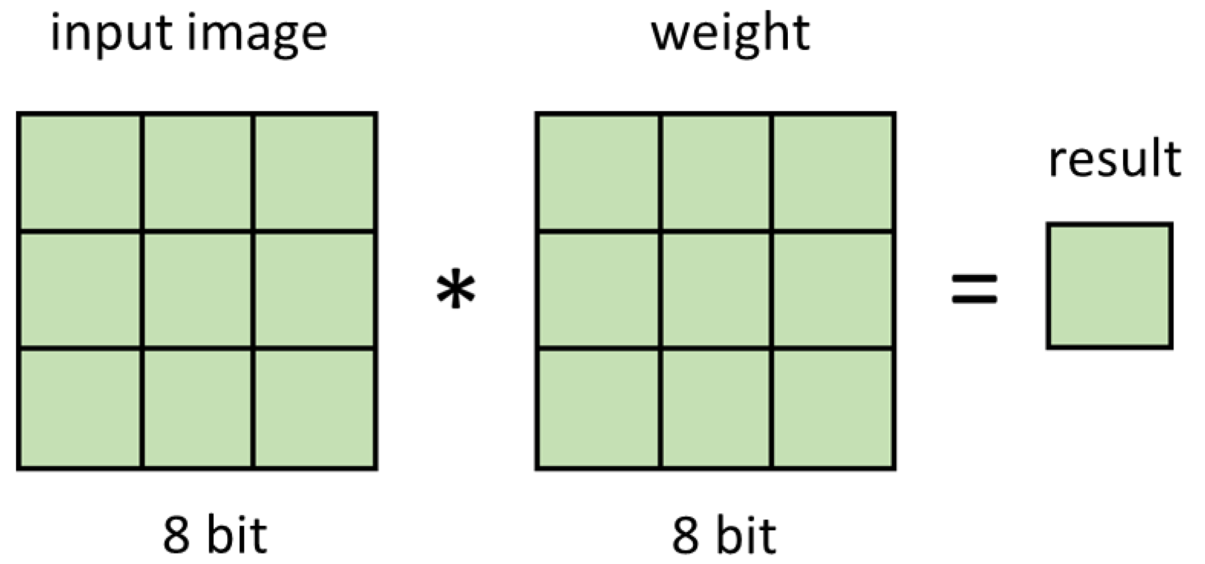
The convolutional layer is the main layer of a CNN. Each output pixel is connected to a local region of the input layer; this connection is called the receptive field. The receptive field can be defined as the window size of the region in the local input that produces a feature. These connections scan the entire image in the input feature map by extending a fixed-size window along the length and width of the entire image. The displacement of the window (i.e., the overlap of the receptive fields in both the height and width) typically has a value of 1 and is shared with the kernel weight. The processes of convolution is a 2D operation in which the shared kernel weight is multiplied element-wise with the corresponding receptive field. These element-wise operations require numerous executions of the multiplication and addition operations.
An input layer typically contains multiple channels, and the sum of all the channels is the result of the convolution. Pixel
y at position
in the convolution result for
n is given as follows.
Therefore, if input data are extended to three dimensions of length, width, and depth, each 2D kernel must correspond to a depth.
The pooling layer can reduce the results of feature extraction but retain important features, typically reducing the image size by half. The pooling layer is generally placed following the convolutional layers. Average pooling and max pooling are two common pooling methods. In average pooling, the average value of the local field in each input feature map is calculated, whereas in max pooling, the maximum of the local field parameter is selected and pixels are output. Moreover, the number of output feature maps in the pooling layer must be equal to the number of input feature maps. Reducing the parameters can increase the efficiency of system operations; thus, a pooling layer is typically used when building neural networks.
The pooling layer is typically follows the convolutional layer, and the fully connected layer generally constitutes the final layers. The fully connected layer is usually a classifier that flattens the result to one dimension by converting it into a single vector that is used as the input of the next layer. The weight of the next FC layer is used to predict the correct label, and the output of the last fully connected layer is the final probability of each label.
Each of the three CNN layer can perform useful calculations; thus, our research combined these three layers to construct a highly accurate CNN model.
2.2. Spin-Orbit Torque MRAM
Spin-orbit torque MRAM (SOT-MRAM) [
10] is the generation of MRAM following spin transfer torque MRAM (STT-MRAM). The main difference between STT-MRAM and SOT-MRAM is that SOT-MRAM uses a more energy-efficient material called spin hall metal (SHM). SHM causes a rotating Hall effect on the application of a write current; this Hall effect creates a spin-torque switch on the magnetic channel of the free layer. SOT-MRAM does not require substantially more write current than STT-MRAM does because the area in which the current flows through SHM is relatively small. SOT-MRAM also has separate read and write paths, which can improve read and write speeds. Thus, we used SOT-MRAM circuit architecture.
An SOT-MRAM cell comprises two word lines, namely the read word line (RWL) and write word line (WWL); two bit lines, namely the read bit line (RBL) and write bit line (WBL); one source line (SL); and two access transistors. The details of SOT-MRAM operation are as follows.
On a rising write signal, the write current from the WBL flows in, and the WWL signal simultaneously activates the access transistor. Thus, the write current can flow through the access transistor. For a written value of 0(1), the current changes from SL(WBL) to WBL(SL). The direction of the free layer’s magnetic field can be changed by the spin Hall effect, which is generated by the different current directions.
If the direction of the changed magnetic field is parallel (anti-parallel) to the fixed magnetic field, the effective resistance of the MTJ is (), which has low (high) impedance. By connecting SL to GND and connecting the switch voltage source () to WBL, the direction of the write current can be changed directly.
On a rising read signal, the induced current passes through RBL. The sensing current then passes through the bit cell when the RWL signal switches on the transistor on the RBL side. To read the bit cell, the sense amplifier senses the voltage of the BL. The sensed current and the resistance of the bit cell are known when SL is grounded. Finally, the voltage value of BL can be calculated by the product of the sensing current and the effective resistance ( and ) of the unit.
2.3. Memory Comparison
Table 1 presents the characteristics of different types of memory for comparison [
11]. The read/write speed of MRAM is similar to that of SRAM and DRAM, but the read power consumption is substantially lower than both DRAM and SRAM. In addition, MRAM is nonvolatile memory; thus, MRAM does not consume any energy outside of I/O operations, and data are not lost when power is disconnected. MRAM also has advantages in its manufacture over DRAM and SRAM in that it can be combined with an original digital circuit by adding a masking layer. In the future, MRAM may be able to replace the cache or flash memory in microcomputer units (MCUs). Therefore, MRAM is suitable for the design of CIM circuit architecture.
2.4. Computing Bit-Wise Logical Operations in SOT-MRAM
2.4.1. Energy Efficient Method of AND/OR Operations in SOT-MRAM
A physics-based compact model for a three terminal PMTJ is proposed in [
12], which models the magnetic, electrical, and thermal behaviors of a PMTJ controlled through SOTs. It considers the effects of both damping-like and field-like SOTs on device behavior. Moreover, the model tackles the dynamic behavior of the self-heating process within the device. However, the compact model does not design in-memory computing architecture for a convolutional neural network based on spin-orbit torque MRAM. After that, an energy efficient method of AND/OR operations in SOT-MRAM [
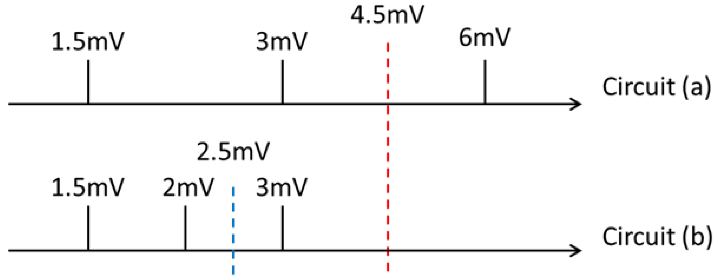
8] is proposed, which is the first generation of MRAM using a changing magnetic field to change its internal resistance to store a bit (0 or 1). When a fixed current is input to read 0 or 1, different voltages can be obtained. Thus, if a current is input to two MRAMs, four different voltages are obtained, as presented in
Figure 1b. The AND and OR results of these two cells can be obtained and can achieve CIM in the design of sensing amplifiers. However, this method of reading two cells simultaneously has disadvantages. As presented in
Table 2, the voltage difference between two cells, namely voltage gap, is approximately 1 mV but can be as low as 0.5 mV. This slight gap is a substantial challenge for designing sense amplifier (SA) and also reduces the robustness of this circuit. Therefore, we adopted the circuit presented in
Figure 1a to overcome this problem.
First, the voltage of the cell is measured. This voltage is used to determine whether the input current is I1 or I0, and the ratio of I1 to I0 is equivalent to the ratio of
to
. As indicated in
Table 3, the voltage difference is larger, and the calculation can, thus, be more robust.
Figure 2 reveals that, for the same read current, the voltage gap required by the circuit of
Figure 1a is greater than
Figure 1b, indicating that the circuit has a greater robustness. Therefore, low current and low power consumption can be used to set the same voltage threshold.
2.4.2. Majority Operation
The majority function returns an output of 1 if more than two signals of the three inputs are 1. The truth table of the majority logic operation is presented in
Table 4. According to
Table 4, the result of majority logic is equivalent to the Cout of a full adder. Therefore, this characteristic can be used to implement a full adder in memory.
2.4.3. Majority Decision in Memory
Kirchhoff’s circuit law indicates that the input current at a node is equal to the output current at a node; this property can be used to implement a current adder. By matching with a corresponding
, the majority result can be obtained, as presented in
Figure 3. Therefore, Cout in memory can be quickly obtained after the majority operation is performed.
2.5. IMCE
IMCE [
5] is a method from a paper published by Angizi et al. in 2018 [
5]. The method uses bitwise in-memory computing to execute calculations. The method requires
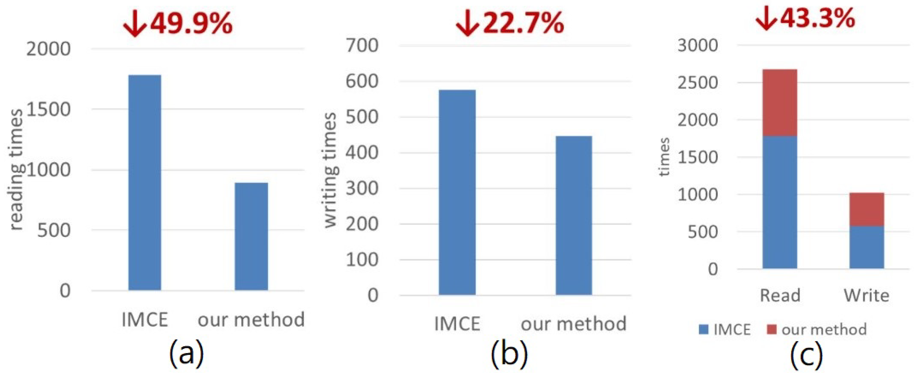
steps to execute an AND operation for a 3-bit value. For each row, a bit count and shift are required. The total is then summed to complete a 4 × 4 convolution. In addition, the bitwise in-memory computing requires additional circuits that increase the power consumption of the critical path. The advantage of the method proposed in this paper is that weight and data are stored in the same memory to facilitate calculation. However, this method requires additional circuits and more cycles to complete the calculation in memory. Overall, the power consumption and critical path of ICME are much greater than those of our method.
2.6. Energy-Efficient CIM Architecture
Kim et al. formulated another method in 2019 [
8]. Their method first executes an AND operation to obtain partial sums, and it then uses a full adder circuit to complete all steps in sequence. If multiple bit lines are executed together, the final result must be calculated through the outer processing of tempsum1 + tempsum2
1. The advantage of the method is that it can run the full adder in memory without the use of additional circuits, but it requires more cycles to complete. The read and write operations must be executed numerous times, and the control of the method is also complicated. These shortcomings cause the data to be read slowly from the CPU, which is partly because the data are stored in the same destination address, meaning that each address can only read one data.
3. Proposed Architecture
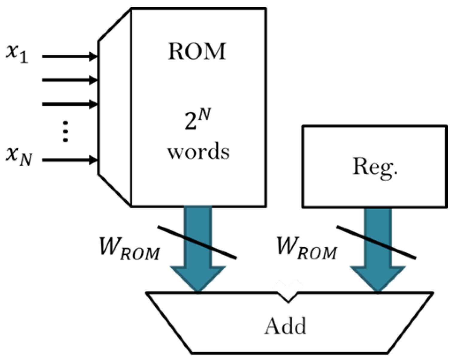
Distributed Arithmetic (DA) was first introduced by Croisier et al. in 1989 [
13]. It is an effective method of operations based on memory access and is effectively a bit-serial operation. The execution time depends on the clock speed, read/write speed of the memory, and the length of the operation bit.
Figure 4 presents a DA circuit.
Let us consider the convolution of two N-point vectors
and a fixed coefficient vector
h, which is expressed as follows:
where
and the input vector os
. Let us assume that
is expressed in B-bit two’s complement representation as follows.
By substituting (3) in (4), the output
y can be expressed in an expanded form as follows.
Because
is constant, there exist
possibilities for
for
. However, these values can be calculated and stored in memory ahead of time. Thus, we can obtain a partial sum by the bit sequence as the address of the read memory. Therefore, the inner product can be calculated through an accumulation loop of B shifter-adders and by reading the value of the corresponding bit sequence. In our method, DA and the CIM structure are combined to overcome the challenges of the aforementioned model [
14].
3.1. Integral Architecture
Figure 5 presents a memory circuit comprising eight banks. Each bank comprises 16 mats, and each mat has four cell arrays of size 16 × 1024 for a total of 1 megabyte. The control circuit can only control eight banks simultaneously. Each operation can run 16 parallel mats operations, and each mat has 4 cell arrays. In addition, each cell array can perform four 3 × 3 convolutions simultaneously; thus, the memory architecture can execute 64 convolutions in parallel.
3.2. Achievements Made by the New Architecture
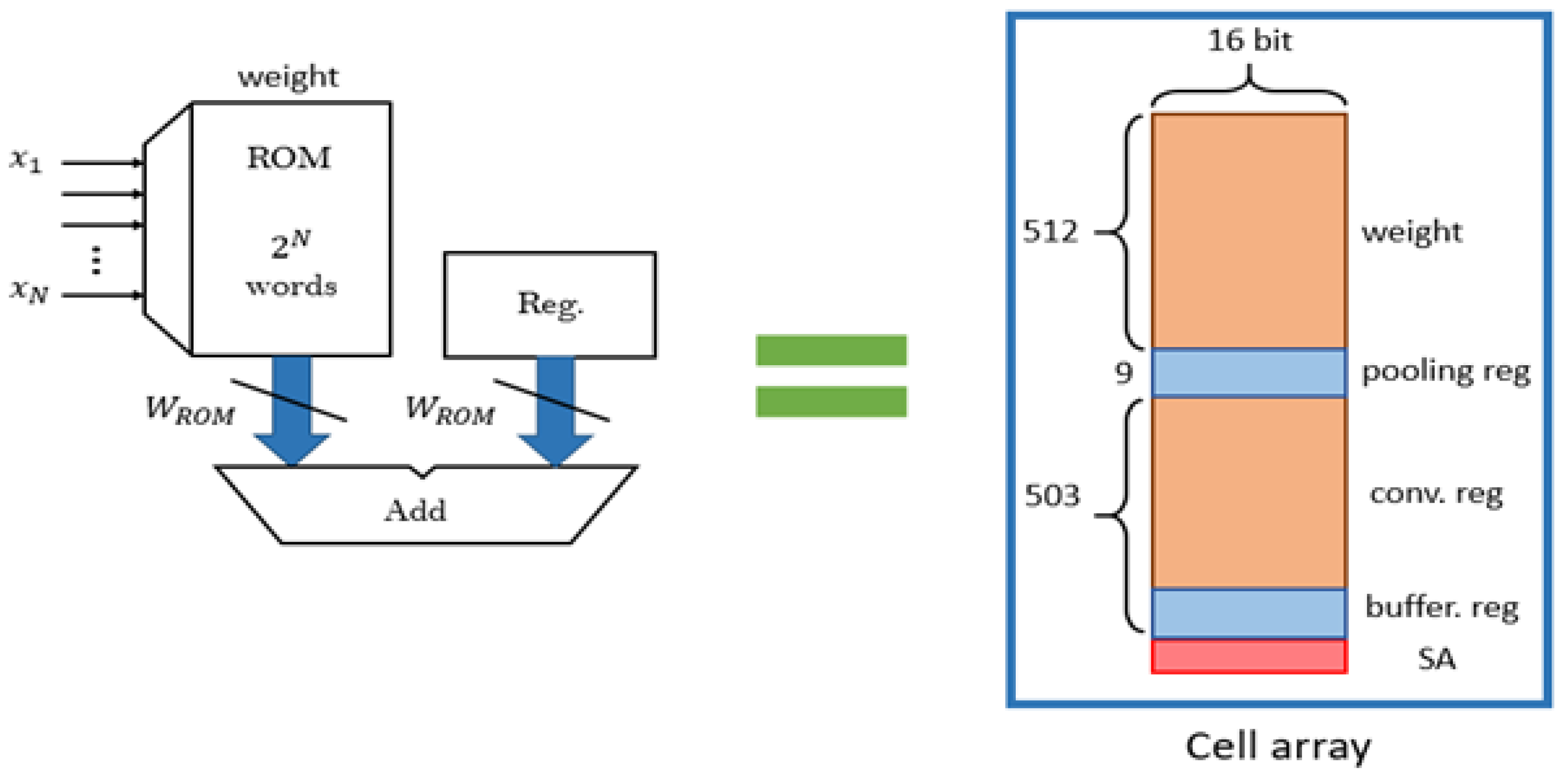
Figure 6 presents our proposed CIM circuit architecture integrating a DA circuit architecture in memory without any digital circuits, such as a full adder or shifter circuit, to implement a DA calculation algorithm. In addition, the CIM architecture requires no additional weighting data; correspondingly, placing the results data and the buffer register on the same cell array can reduce both data access time and power consumption. The execution speed depends on the clock frequency, read speed of memory, and length of the calculation unit. Therefore, the novel CIM architecture performs faster than the traditional DA architecture and has lower power consumption because of the operations performed in memory.
Due to the advantages of the DA algorithm, the precalculated partial sum can be stored in the memory, and the shifter adder can then be used to accumulate the sum of each part. Therefore, our approach uses only a shifter adder and does not require a multiplier with a long critical path or a large area. Our new CIM architecture avoids the lengthy execution steps and additional circuits required by previous methods.
The main components of the DA architecture circuit are the read-only memory (ROM), reg buffer, full adder, and shifter. The following section describes the structure, operation, and implementation of these components to achieve the DA architecture in memory.
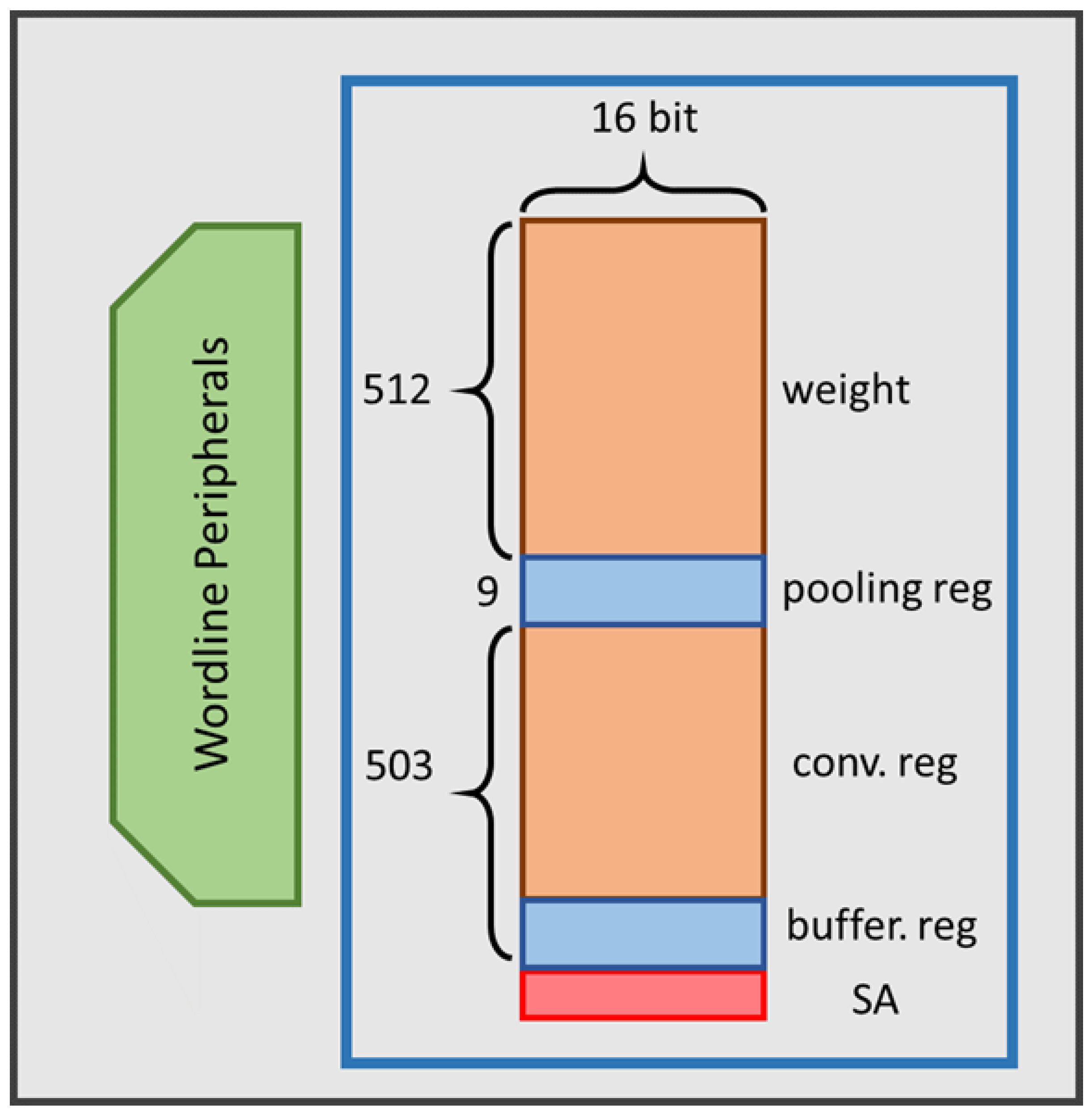
3.2.1. Build ROM and Register (Reg) Buffer in the Memory
MRAM is nonvolatile memory, and its read speed is similar to that of DRAM; thus, MRAM is suitable as the storage unit for a DA architecture. To increase the efficiency of in-memory calculation execution and to achieve lower latency and read/write power consumption, the weighted memory and buffer register stored in the CIM are placed on the same cell array shown, as presented in
Figure 7. In addition, these defined memory sizes can be changed because the entire memory space, not only one specific part of the memory, can complete CIM operations.
3.2.2. Shifter
Because the shifter is unavailable in traditional memory, our method adds N-Metal-Oxide Semiconductor (NMOS) and P-Metal-Oxide Semiconductor (PMOS) to the SA circuit architecture, as presented in
Figure 8. This change enables the output of the SA to be written into different columns based on shifter control without reading data out of the cell array or rewriting; these processes would otherwise extend the read/write time.
3.2.3. Shifter Full-Adder
This unit is used to complete a full adder operation. First, it calculates MAJ(A,B,Cin) to obtain Cout and obtain a sum in parallel in the following step. Then,
is performed to obtain sum-reg. Finally, the left shift to the sum is executed for the next shift-adder operation, as presented in
Figure 9.


