
A Review on SIW and Its Applications to Microwave Components


Abstract
1. Introduction
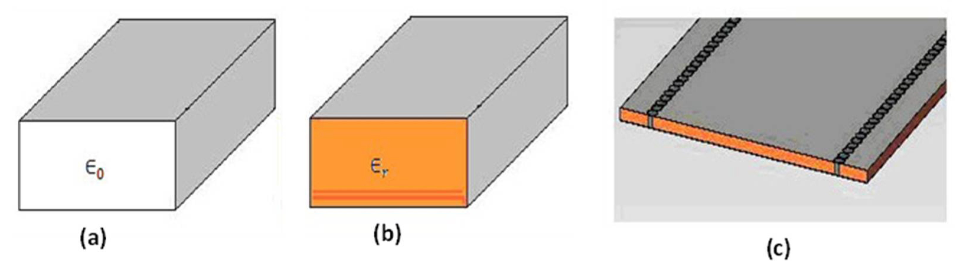
2. Modes in SIW
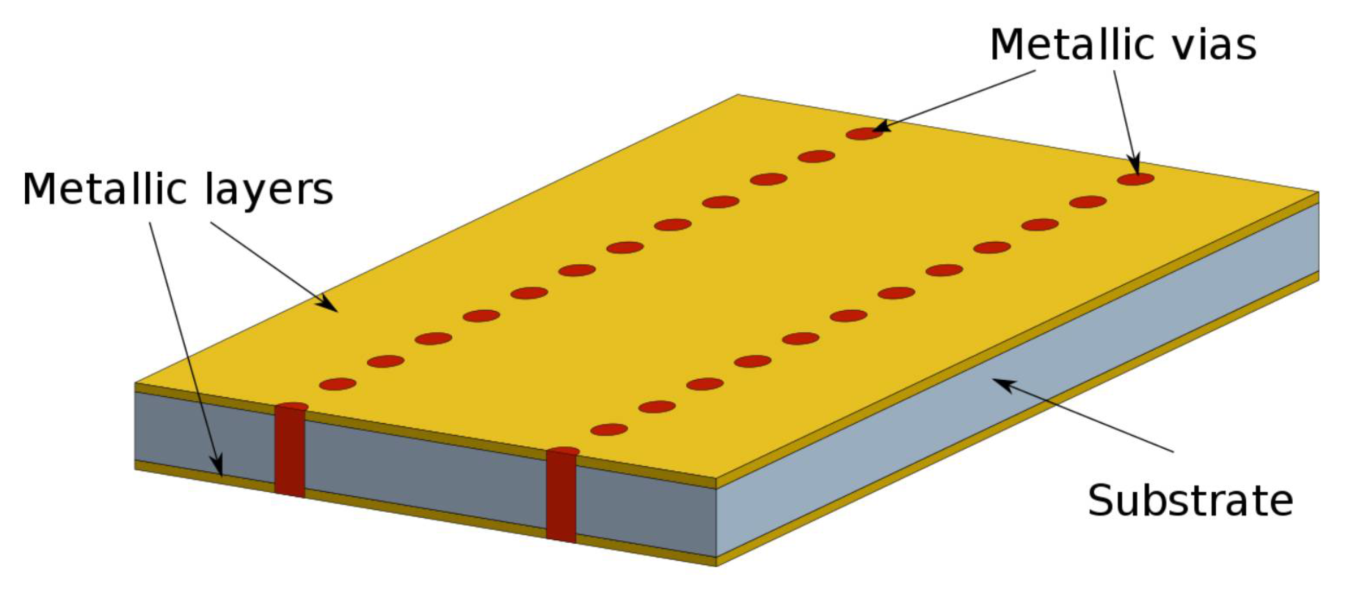
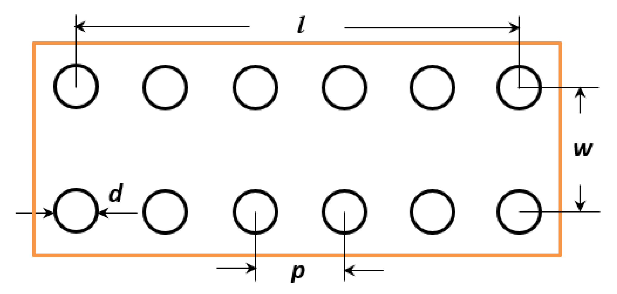
3. SIW Design Basics
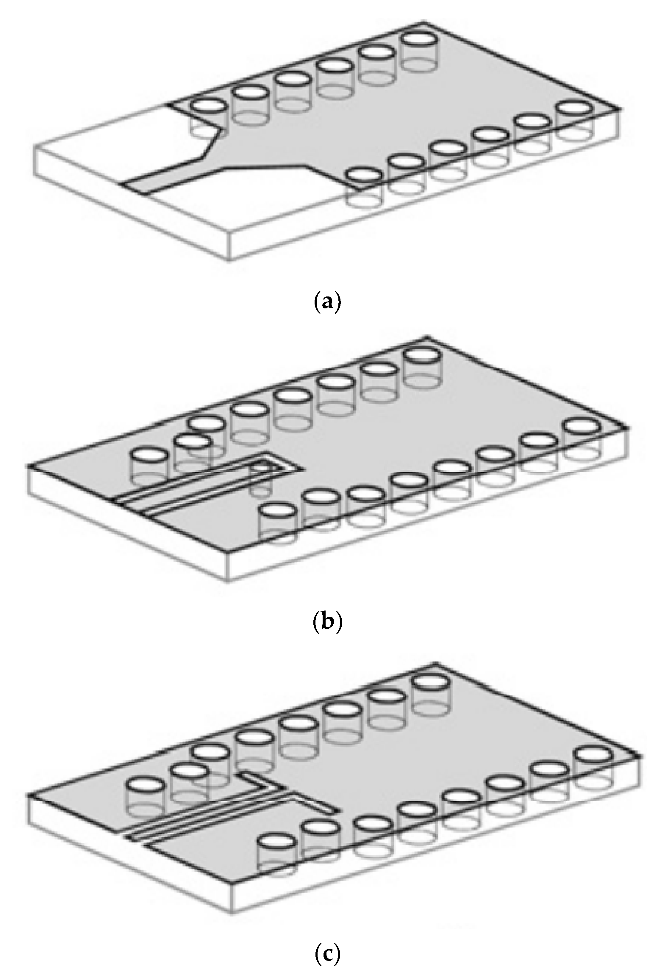
4. Transitions in SIW
5. Losses in Substrate-Integrated Waveguides
6. Performance Attributes of the SIW
- A stress assessment should be performed to obtain the physical change in dimensions in connection with environment temperature as the input;
- A full-wave field assessment should be conducted to verify the frequency shift versus the changes in the physical dimension and selected substrate permittivity;
- A redesign of the given device/component by compensating for the adjustments in the electrical parameters.
- A full-wave field assessment should be conducted to establish the power dissipation and its allocation;
- The dispersed power should be employed in the performance of a thermal assessment and the temperature increase and local hot spots established;
- A comparison of the worst-case values to the glass transition temperature of the substrate at which the material adjusts its performance from being glassy to being rubbery;
- The determination and application of the safety limits;
- A stress assessment should be performed to achieve the physical dimensional adjustment for the temperature allocation under extreme mean power;
- A full-wave field assessment should be conducted to establish the frequency shift along with the shift in bandwidth and return loss, using the revised dimension and substrate permittivity,
- A redesign of the given device/component by compensating for the adjustments in the electrical parameters.
7. Substrate Selection for SIW Implementation
- The physical size of an SIW device is directly linked to the permittivity or dielectric constant of the material used for the device implementation. The higher the material dielectric constant, the smaller the physical size of the SIW device.
- The amount of insertion loss observed in an SIW device relates to three factors: substrate thickness, dielectric loss, and copper foil.
- Thermal expansion and thermal coefficient of permittivity of a substrate material determines the temperature stability of an SIW device.
- SIW components are well known for their good power handling capabilities. The average power handling capability is based on the substrate thermal expansion, the thermal coefficient of permittivity, the thermal conductivity, and the glass transition temperature, while the peak power handling capability is only linked to the substrate dielectric strength.
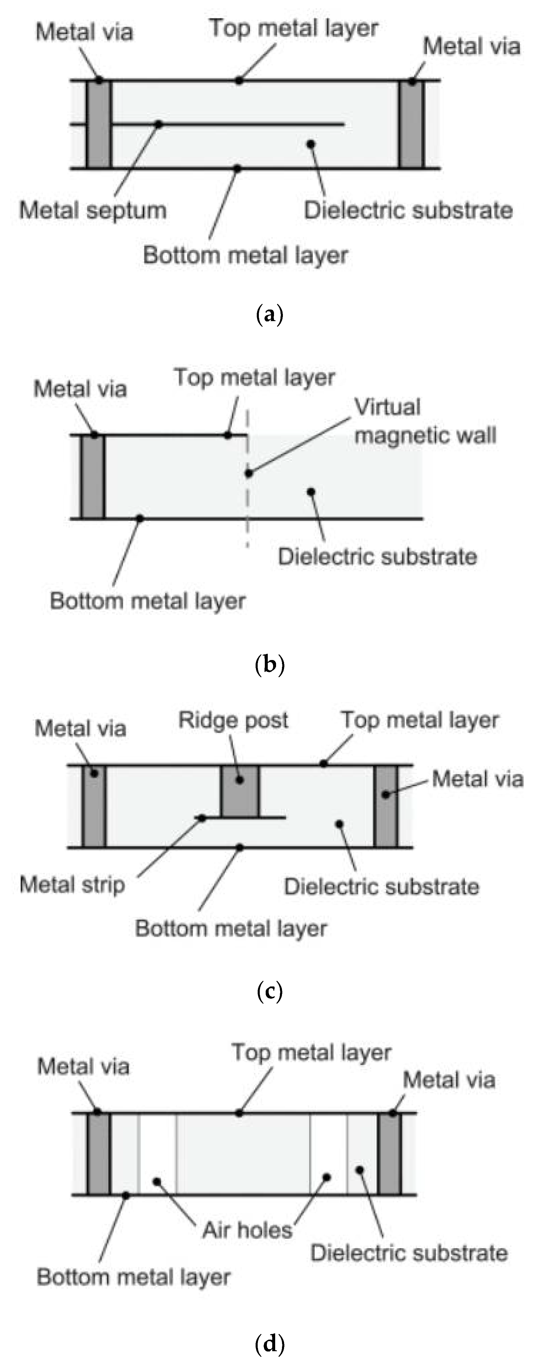
8. Evolutionary Structures of the SIW
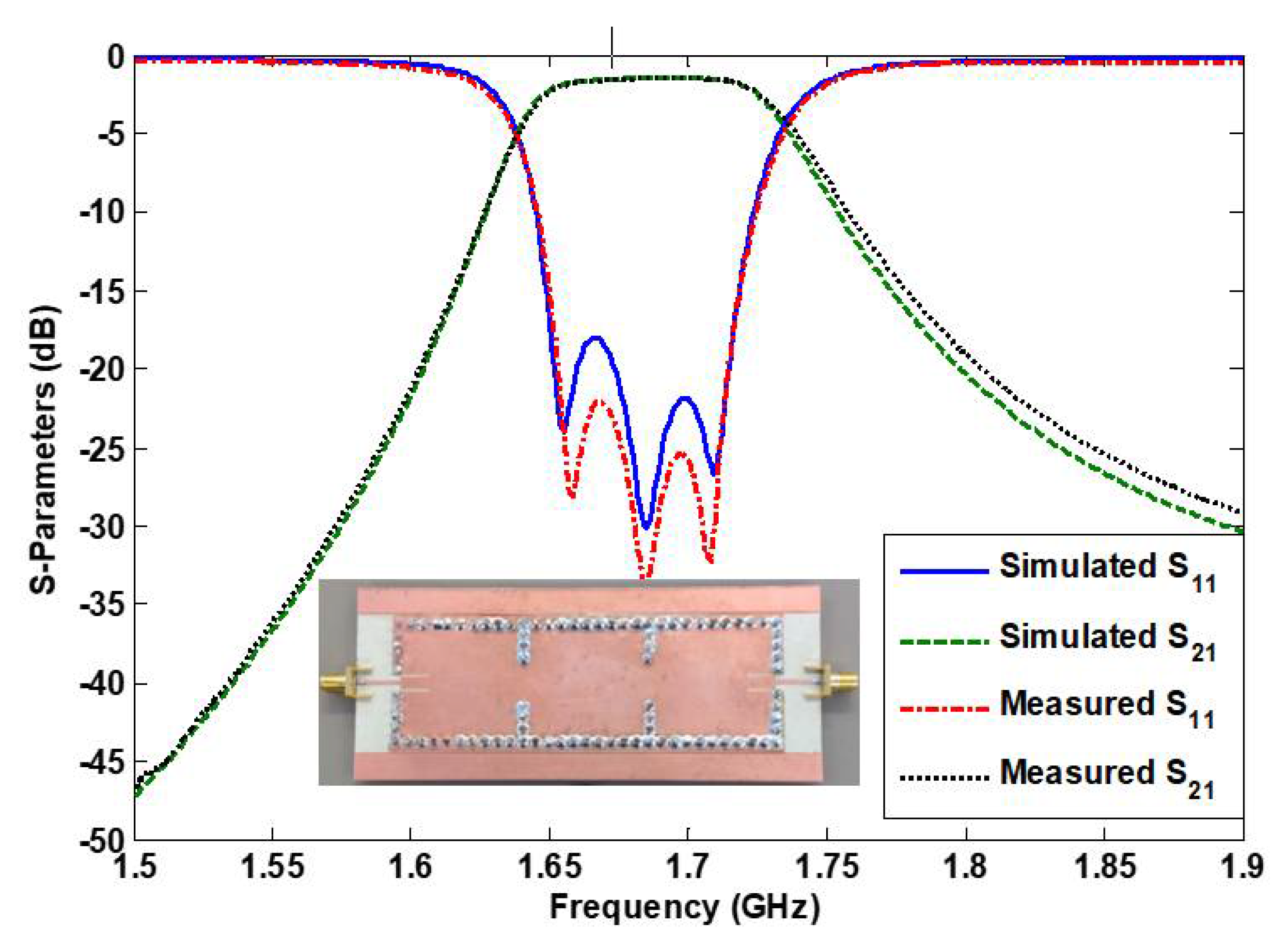
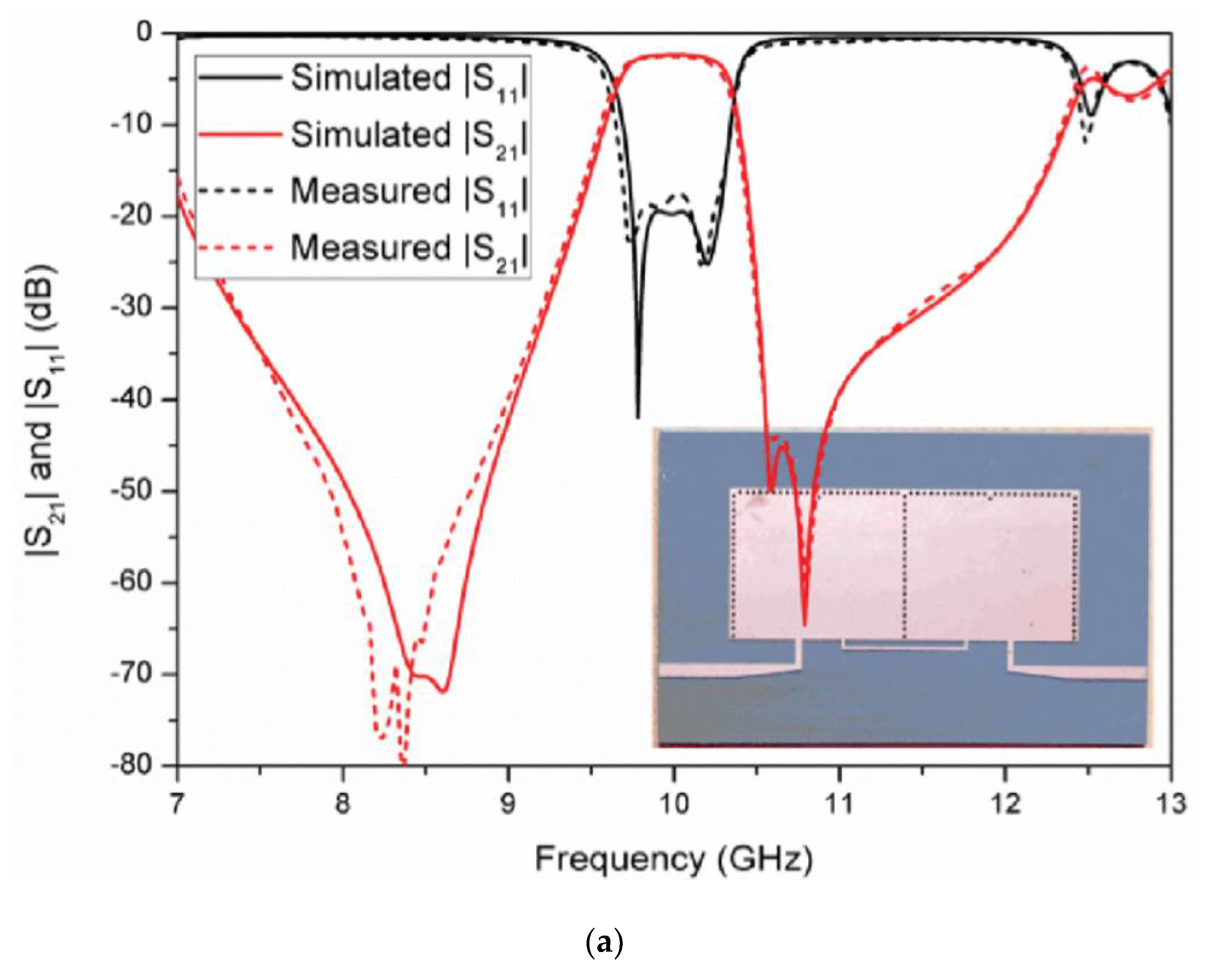
9. SIW Filter
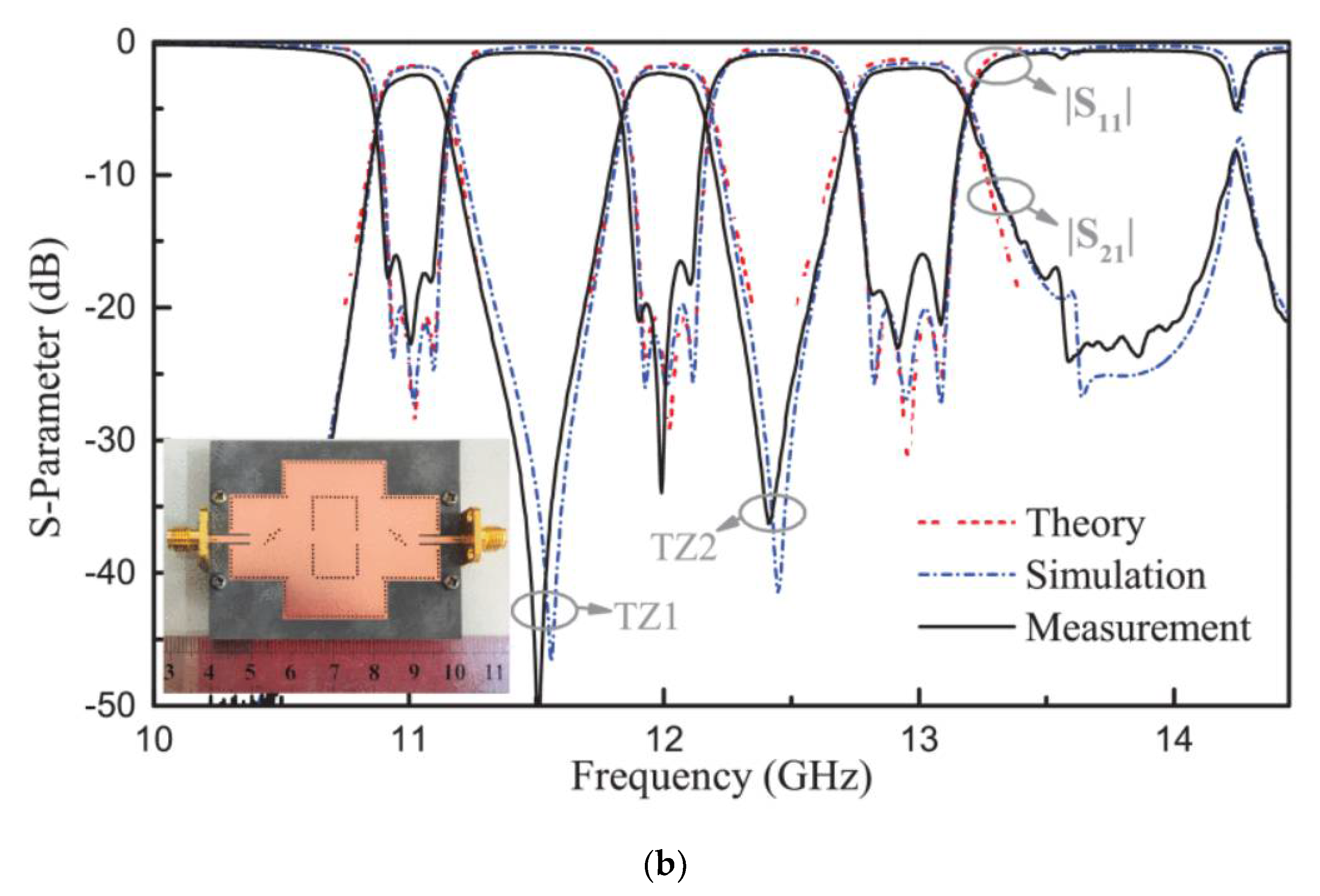
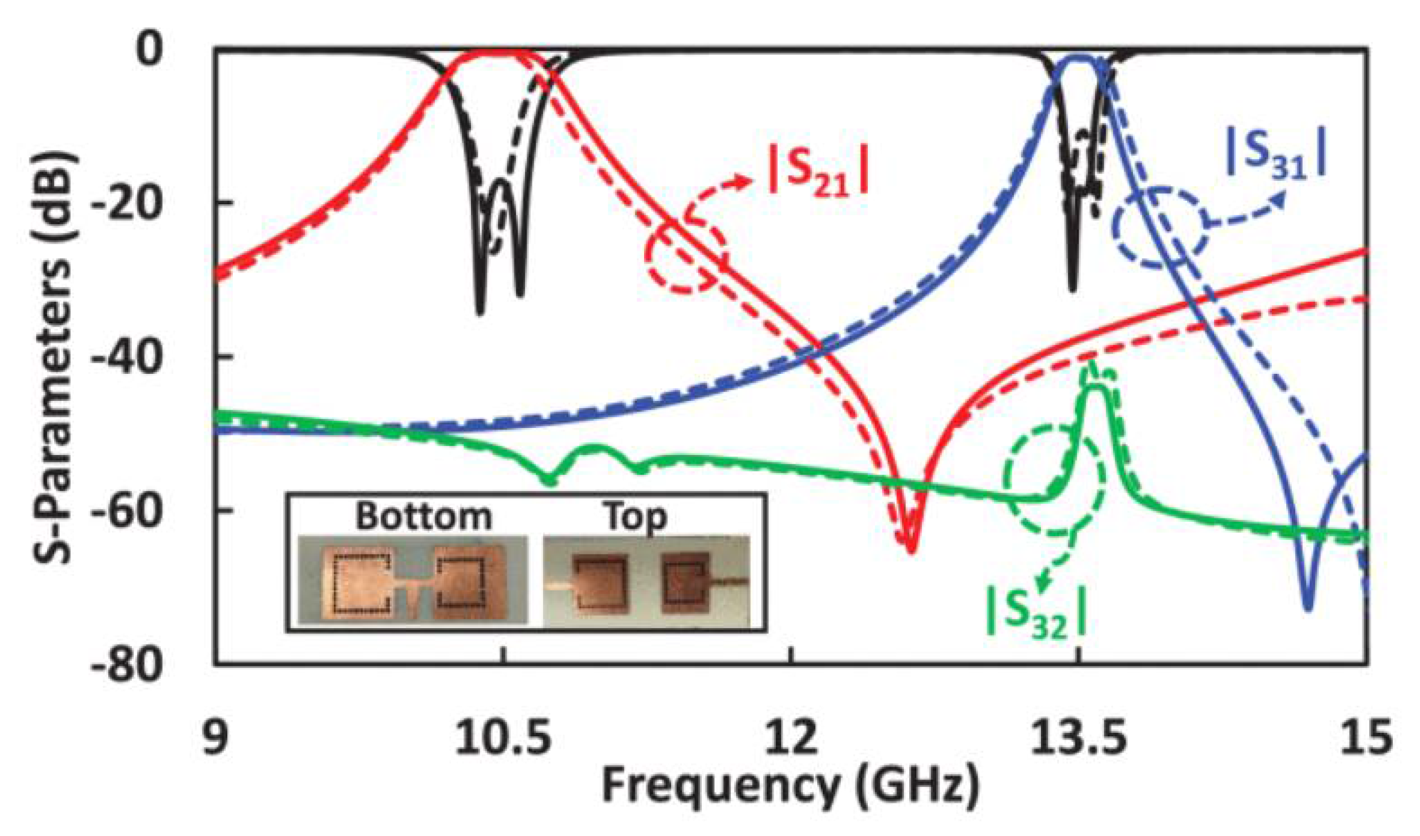
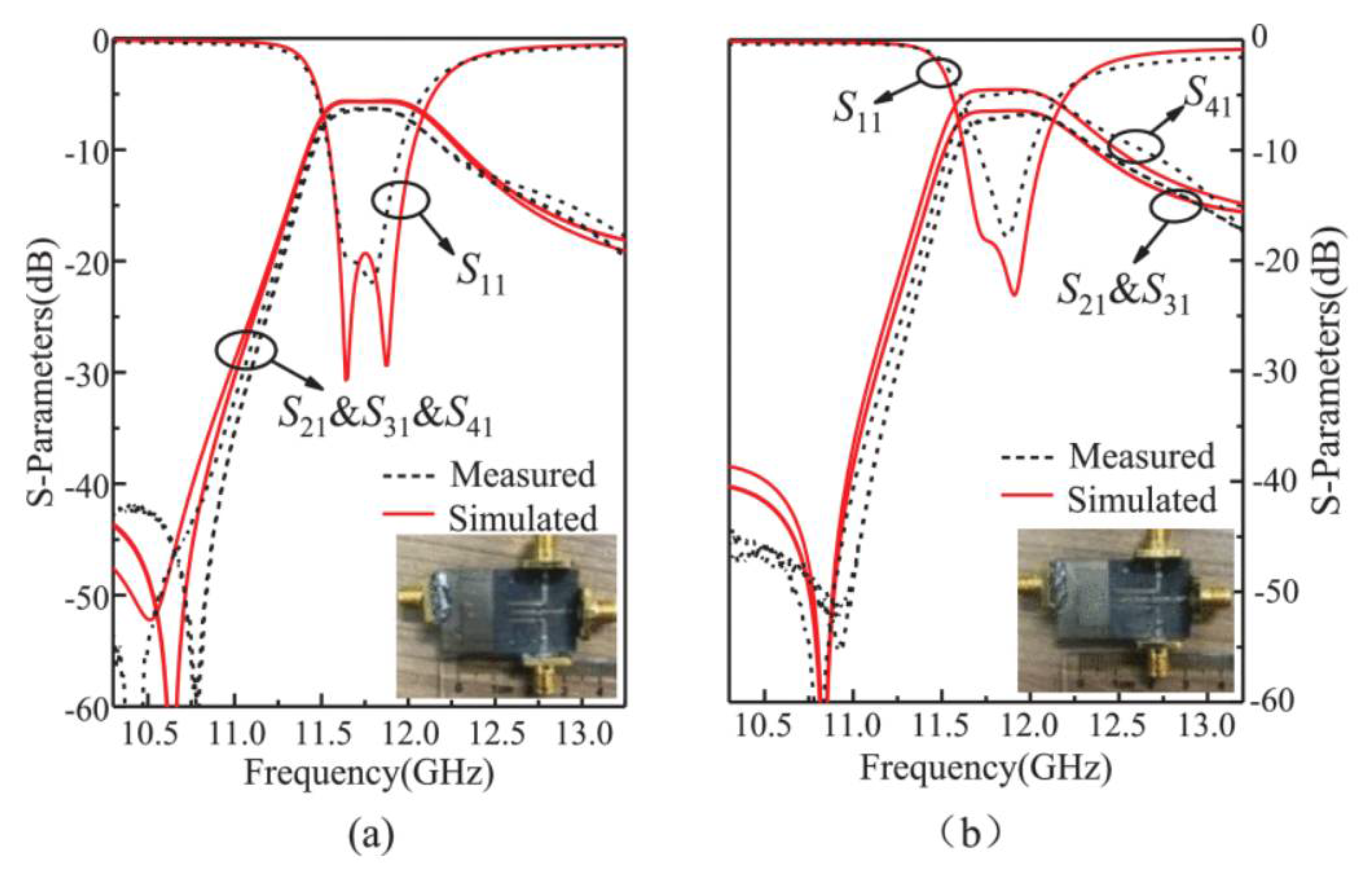
10. SIW Multiplexer
11. SIW Power Divider/Combiner
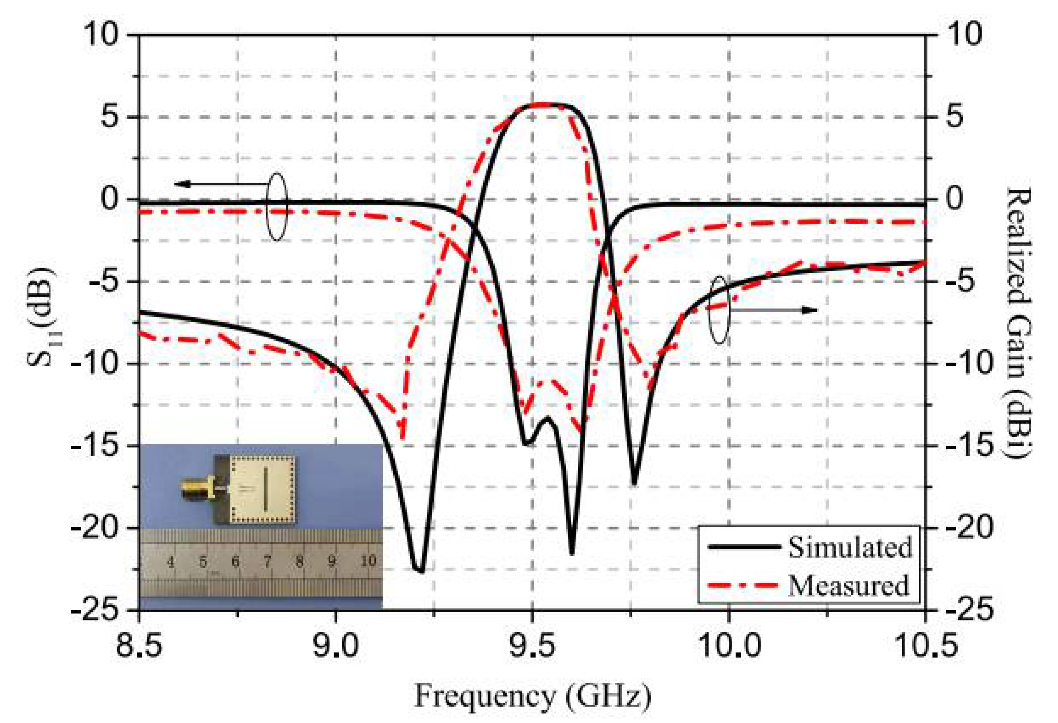
12. SIW Antennas
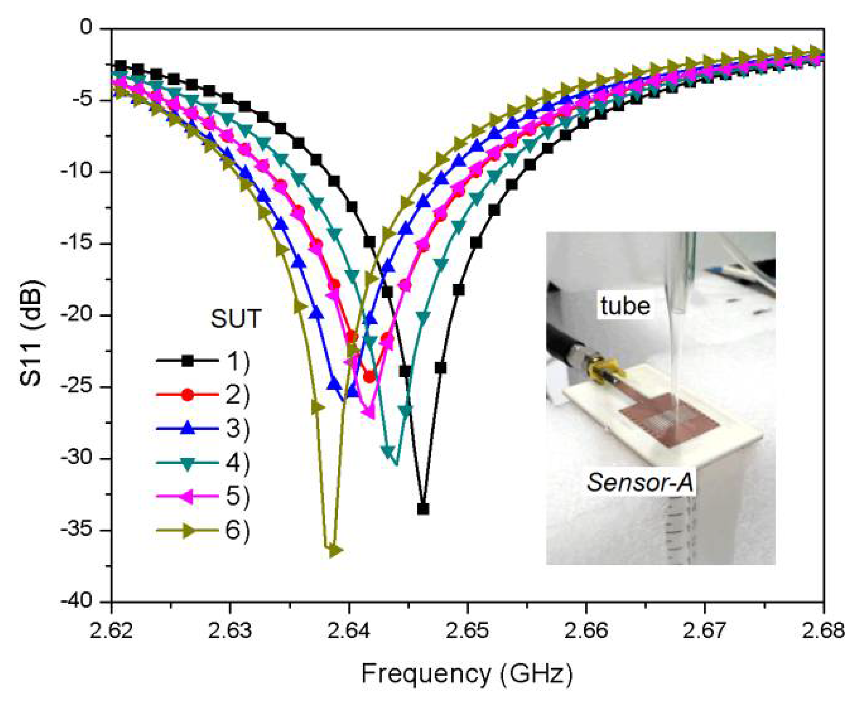
13. SIW Sensors
14. Future Challenges of SIW
15. Conclusions
Author Contributions
Funding
Conflicts of Interest
References
- Chen, X.-P.; Wu, K. Substrate integrated waveguide filter: Basic design rules and fundamental structure features. IEEE Microw. Mag. 2014, 15, 108–116. [Google Scholar] [CrossRef]
- Hong, J.-S. Microstrip Filters for RF/Microwave Applications, 2nd ed.; Wiley: New York, NY, USA, 2011; pp. 1–635. [Google Scholar]
- Nwajana, A.O.; Yeo, K.S.K. Practical Approach to Substrate Integrated Waveguide (SIW) Diplexer: Emerging Research and Opportunity, 1st ed.; IGI Global: Hershey, PA, USA, 2020; pp. 1–171. [Google Scholar]
- Deslandes, D.; Wu, K. Design consideration and performance analysis of substrate integrated waveguide components. In Proceedings of the 32nd European Microwave Conference (EuMC), Milan, Italy, 27–29 September 2002; IEEE: Piscataway, NJ, USA, 2002; pp. 23–26. [Google Scholar]
- Cassivi, Y.; Perregrini, L.; Arcioni, P.; Bressan, M.; Wu, K.; Conciauro, G. Dispersion characteristics of substrate integrated rectangular waveguide. IEEE Microw. Wirel. Compon. Lett. 2002, 12, 333–335. [Google Scholar] [CrossRef]
- Nwajana, A. Analysis and Design of a Substrate Integrated Waveguide Multi-Coupled Resonator Diplexer. Ph.D. Thesis, University of East London, London, UK, July 2017; pp. 1–175. [Google Scholar]
- Deslandes, D.; Wu, K. Single-substrate integrated technique of planar circuits and waveguide filters. IEEE Trans. Microw. Theory Tech. 2003, 51, 593–596. [Google Scholar] [CrossRef]
- Venanzoni, G.; Mencarelli, D.; Morini, A.; Farina, M.; Prudenzano, F. Review of substrate integrated waveguide circuits for beam-forming networks working in X-band. Appl. Sci. 2019, 9, 1003. [Google Scholar] [CrossRef]
- Wu, K. Integration and interconnect techniques of planar and nonplanar structures for microwave and millimeter-wave circuits: Current status and future trend. In Proceedings of the 2001 Asia-Pacific Microwave Conference (APMC), Taipei, Taiwan, 3–6 December 2001; IEEE: Piscataway, NJ, USA, 2002; pp. 411–416. [Google Scholar]
- Nwajana, A.O.; Yeo, K.S.K.; Dainkeh, A. Low cost SIW Chebyshev bandpass filter with new input/output connection. In Proceedings of the 16th Mediterranean Microwave Symposium (MMS), Abu Dhabi, UAE, 14–16 November 2016; IEEE: Piscataway, NJ, USA, 2017; pp. 1–4. [Google Scholar]
- Cheng, Y.J. Substrate Integrated Antennas and Arrays, 1st ed.; CRC Press: New York, NY, USA, 2015; pp. 1–256. [Google Scholar]
- Han, S.H.; Wang, X.L.; Fan, Y.; Yang, Z.Q.; He, Z.N. The generalized Chebyshev substrate integrated waveguide diplexer. Prog. Electromagn. Res. 2007, 73, 29–38. [Google Scholar] [CrossRef]
- Deslandes, D.; Wu, K. Accurate modelling, wave mechanisms, and design considerations of a substrate integrated waveguide. IEEE Trans. Microw. Theory Tech. 2006, 54, 2516–2526. [Google Scholar] [CrossRef]
- Bozzi, M.; Georgiadis, A.; Wu, K. Review of substrate-integrated waveguide circuits and antennas. IET Microw. Antennas Propag. 2011, 5, 909–920. [Google Scholar] [CrossRef]
- Xu, F.; Wu, K. Guided-wave and leakage characteristics of substrate integrated waveguide. IEEE Trans. Microw. Theory Tech. 2005, 53, 66–73. [Google Scholar]
- Chen, X.; Hong, W.; Cui, T.; Wu, K. Substrate integrated waveguide (SIW) linear phase filter. IEEE Microw. Wirel. Compon. Lett. 2005, 15, 787–789. [Google Scholar] [CrossRef]
- Nwajana, A.O.; Dainkeh, A.; Yeo, K.S.K. Substrate integrated waveguide (SIW) diplexer with novel input/output coupling and no separate junction. Prog. Electromagn. Res. M 2018, 67, 75–84. [Google Scholar] [CrossRef][Green Version]
- Deslandes, D. Design equations for tapered microstrip-to-substrate integrated waveguide transitions. In Proceedings of the IEEE MTT-S International Microwave Symposium (IMS) Digest, Anaheim, CA, USA, 23–28 May 2010; pp. 704–707. [Google Scholar]
- Deslandes, D.; Wu, K. Integrated microstrip and rectangular waveguide in planar form. IEEE Microw. Wirel. Compon. Lett. 2001, 11, 68–70. [Google Scholar] [CrossRef]
- Deslandes, D.; Wu, K. Integrated transition of coplanar to rectangular waveguides. In Proceedings of the IEEE MTT-S International Microwave Symposium (IMS) Digest, Phoenix, AZ, USA, 20–25 May 2001; pp. 619–622. [Google Scholar]
- Deslandes, D.; Wu, K. Analysis and design of current probe transition from grounded coplanar to substrate integrated rectangular waveguides. IEEE Trans. Microw. Theory Tech. 2005, 53, 593–596. [Google Scholar] [CrossRef]
- Huang, Y.; Wu, K.L. A broad-band LTCC integrated transition of laminated waveguide to air-filled waveguide for millimeter-wave applications. IEEE Trans. Microw. Theory Tech. 2003, 51, 1613–1617. [Google Scholar] [CrossRef]
- Xia, L.; Xu, R.; Yan, B.; Li, J.; Guo, Y.; Wang, J. Broadband transition between air-filled waveguide and substrate integrated waveguide. Electron. Lett. 2006, 42, 1403–1405. [Google Scholar] [CrossRef]
- Ding, Y.; Wu, K. Substrate integrated waveguide-to-microstrip transition in multilayer substrate. IEEE Trans. Microw. Theory Tech. 2007, 55, 2839–2844. [Google Scholar] [CrossRef]
- Bozzi, M.; Pasian, M.; Perregrini, L.; Wu, K. On the losses in substrate-integrated waveguides and cavities. Int. J. Microw. Wirel. Technol. 2009, 1, 395–401. [Google Scholar] [CrossRef]
- Bozzi, M.; Perregrini, L.; Wu, K. Modeling of conductor, dielectric, and radiation losses in substrate integrated waveguide by the boundary integral-resonant mode expansion method. IEEE Trans. Microw. Theory Tech. 2008, 56, 3153–3161. [Google Scholar] [CrossRef]
- Bozzi, M.; Perregrini, L.; Wu, K. Modeling of losses in substrate integrated waveguide by the boundary integral-resonant mode expansion method. In Proceedings of the IEEE MTT-S International Microwave Symposium (IMS) Digest, Atlanta, GA, USA, 15–20 June 2008; pp. 515–518. [Google Scholar]
- Ranjkesh, N.; Shahabadi, M. Loss mechanism in SIW and MSIW. Prog. Electromagn. Res. B 2008, 4, 299–309. [Google Scholar] [CrossRef]
- Bozzi, M.; Pasian, M.; Perregrini, L.; Wu, K. On the losses in substrate integrated waveguides. In Proceedings of the European Microwave Conference (EuMC), Munich, Germany, 9–12 October 2007; IEEE: Piscataway, NJ, USA, 2007; pp. 384–387. [Google Scholar]
- Bozzi, M.; Pasian, M.; Perregrini, L. Modeling of losses in substrate integrated waveguide components. In Proceedings of the IEEE International Conference on Numerical Electromagnetic Modeling and Optimization for RF, Microwave, and Terahertz Applications (NEMO), Pavia, Italy, 14–16 May 2014; pp. 1–4. [Google Scholar]
- Bozzi, M.; Perregrini, L.; Wu, K.; Arcioni, P. Current and future research trends in substrate integrated waveguide technology. Radioengineering 2009, 18, 201–209. [Google Scholar]
- Pasian, M.; Bozzi, M.; Perregrini, L. Radiation losses in substrate integrated waveguides: A semi-analytical approach for a quantitative determination. In Proceedings of the IEEE MTT-S International Microwave Symposium (IMS) Digest, Seattle, WA, USA, 2–7 June 2013; pp. 1–3. [Google Scholar]
- Chen, X.-P.; Wu, K. Substrate integrated waveguide filter: Practical aspects and design considerations. IEEE Microw. Mag. 2014, 15, 75–83. [Google Scholar] [CrossRef]
- Wang, C. Temperature compensations for microwave resonators and filters. In Proceedings of the IEEE MTT-S International Microwave Symposium (IMS) Digest, Long Beach, CA, USA, 13–19 June 2005; pp. 1–30. [Google Scholar]
- Djerafi, T.; Wu, K.; Deslandes, D. Temperature drift compensation technique for substrate integrated waveguide oscillator. IEEE Microw. Wirel. Compon. Lett. 2012, 60, 489–491. [Google Scholar] [CrossRef]
- Djerafi, T.; Wu, K.; Deslandes, D. A temperature-compensation technique for substrate integrated waveguide cavities and filters. IEEE Trans. Microw. Theory Tech. 2012, 60, 2448–2455. [Google Scholar] [CrossRef]
- Mansour, R.R.; Jolley, B.; Ye, S.; Thomson, F.S.; Dokas, V. On the power handling capability of high temperature superconductive filters. IEEE Trans. Microw. Theory Tech. 1996, 44, 1322–1338. [Google Scholar] [CrossRef]
- Yu, M. Power-handling capability for RF filters. IEEE Microw. Mag. 2007, 8, 88–97. [Google Scholar] [CrossRef]
- Wu, K.; Bozzi, M.; Fonseca, N.J.G. Substrate integrated transmission lines: Review and applications. IEEE J. Microw. 2021, 1, 345–363. [Google Scholar] [CrossRef]
- Bozzi, M.; Perregrini, L.; Tomassoni, C. A review of compact substrate integrated waveguide (SIW) interconnects and components. In Proceedings of the IEEE 23rd Workshop on Signal and Power Integrity (SPI), Chambéry, France, 18–21 June 2019; pp. 1–4. [Google Scholar]
- Wang, Z.; Shen, D.; Xu, R.; Yan, B.; Lin, W.; Guo, Y.; Xie, X. Partial H-plane bandpass filters based on substrate integrated folded waveguide (SIFW). In Proceedings of the IEEE Asia Pacific Microwave Conference (APMC), Singapore, 7–10 December 2009; pp. 1–4. [Google Scholar]
- Grigoropoulos, N.; Sanz-Izquierdo, B.; Young, P.R. Substrate integrated folded waveguides (SIFW) and filters. IEEE Microw. Wirel. Compon. Lett. 2005, 15, 829–831. [Google Scholar] [CrossRef]
- Wang, Z.; Bu, S.; Luo, Z. A substrate integrated folded waveguide (SIFW) H-plane band-pass filter with double H-plane septa based on LTCC. IEEE Trans. Ultrason. Ferroelectr. Freq. Control. 2012, 59, 560–563. [Google Scholar] [CrossRef]
- Zhai, G.H.; Hong, W.; Wu, K.; Chen, J.X.; Chen, P.; Tang, H.J. Substrate integrated folded waveguide (SIFW) narrow-wall directional coupler. In Proceedings of the IEEE International Conference on Microwave and Millimeter Wave Technology, Nanjing, China, 21–24 April 2008; pp. 1–4. [Google Scholar]
- Moro, R.; Moscato, S.; Bozzi, M.; Perregrini, L. Substrate integrated folded waveguide filter with out-of-band rejection controlled by resonant-mode suppression. IEEE Microw. Wirel. Compon. Lett. 2015, 25, 214–216. [Google Scholar] [CrossRef]
- Qiu, P.-J.; Wang, Z.-G.; Yan, B. Novel Ka-band substrate integrated folded waveguide (SIFW) Quasi-elliptic filters in LTCC. In Proceedings of the IEEE Asia Pacific Microwave Conference (APMC), Hong Kong, China, 16–20 December 2008; pp. 1–4. [Google Scholar]
- Alotaibi, S.K.; Hong, J.-S. Substrate integrated folded-waveguide filter with asymmetrical frequency response. In Proceedings of the 38th European Microwave Conference (EuMC), Amsterdam, The Netherlands, 27–31 October 2008; IEEE: Piscataway, NJ, USA, 2008; pp. 1002–1005. [Google Scholar]
- Chien, H.-Y.; Shen, T.-M.; Hung, T.-Y.; Wu, R.-B. Design of a vertically stacked substrate integrated folded-waveguide resonator filter in LTCC. In Proceedings of the IEEE Asia Pacific Microwave Conference (APMC), Bangkok, Thailand, 11–14 December 2007; pp. 1–4. [Google Scholar]
- Zhu, F.; Luo, G.Q.; Liao, Z.; Dai, X.W.; Wu, K. Compact dual-mode bandpass filters based on half-mode substrate-integrated waveguide cavities. IEEE Microw. Wirel. Compon. Lett. 2021, 31, 441–444. [Google Scholar] [CrossRef]
- Hong, W.; Liu, B.; Wang, Y.; Lai, Q.; Tang, H.; Yin, X.X.; Dong, Y.D.; Zhang, Y.; Wu, K. Half mode substrate integrated waveguide: A new guided wave structure for microwave and millimeter wave application. In Proceedings of the Joint 31st International Conference on Infrared Millimeter Waves and 14th International Conference on Teraherz Electronics, Shanghai, China, 18–22 September 2006; p. 219. [Google Scholar]
- Elobied, A.A.; Yang, X.-X.; Lou, T.; Gao, S. Compact 2 × 2 MIMO antenna with low mutual coupling based on half mode substrate integrated waveguide. IEEE Trans. Antennas Propag. 2021, 69, 2975–2980. [Google Scholar] [CrossRef]
- Peng, Y.; Sun, L. A compact broadband phase shifter based on HMSIW evanescent mode. IEEE Microw. Wirel. Compon. Lett. 2021, 31, 857–860. [Google Scholar] [CrossRef]
- Ji, L.; Li, X.-C.; He, X.; Mao, J.-F. A slow wave ridged half-Mode substrate integrated waveguide with spoof surface plasmon polaritons. IEEE Trans. Plasma Sci. 2021, 49, 1818–1825. [Google Scholar] [CrossRef]
- Javanbakht, N.; Amaya, R.E.; Shaker, J.; Syrett, B. Side-lobe level reduction of half-mode substrate integrated waveguide leaky-wave antenna. IEEE Trans. Antennas Propag. 2021, 69, 3572–3577. [Google Scholar] [CrossRef]
- Javanbakht, N.; Amaya, R.E.; Shaker, J.; Syrett, B. A compact cavity-based leaky-wave antenna in a low temperature co-fired ceramic process with improved performance. IEEE Access 2021, 9, 25014–25024. [Google Scholar] [CrossRef]
- Bozzi, M.; Winkler, S.A.; Wu, K. Broadband and compact ridge substrate-integrated waveguides. IET Microw. Antennas Propag. 2010, 4, 1965–1973. [Google Scholar] [CrossRef]
- Su, Y.; Lin, X.Q.; Fan, Y. Dual-polarized leaky wave antenna with low cross-polarization based on the mode composite ridged waveguide. In Proceedings of the International Conference on Microwave and Millimeter Wave Technology (ICMMT), Shanghai, China, 20–23 September 2020; pp. 1–3. [Google Scholar]
- Che, W.; Li, C.; Zhang, D.; Chow, Y.L. Investigations on propagation and the band broadening effect of ridged rectangular waveguide integrated in a multilayer dielectric substrate. IET Microw. Antennas Propag. 2010, 4, 674–684. [Google Scholar] [CrossRef]
- Liu, Z.; Lin, X.Q.; Su, Y. A novel compact diplexer with high isolation based on the mode composite ridged waveguide. In Proceedings of the International Conference on Microwave and Millimeter Wave Technology (ICMMT), Shanghai, China, 20–23 September 2020; pp. 1–3. [Google Scholar]
- Zhang, F.; Hua, G. Empirical formulas of SIRW and its application in half-mode SIRW hybrid ring coupler design. In Proceedings of the IEEE MTT-S International Wireless Symposium (IWS), Shanghai, China, 20–23 September 2020; pp. 1–3. [Google Scholar]
- Massoni, E.; Bozzi, M.; Wu, K. Increasing efficiency of leaky-wave antenna by using substrate integrated slab waveguide. IEEE Antennas Wirel. Propag. Lett. 2019, 18, 1596–1600. [Google Scholar] [CrossRef]
- Bozzi, M.; Deslandes, D.; Arcioni, P.; Perregrini, L.; Wu, K.; Conciauro, G. Efficient analysis and experimental verification of substrate integrated slab waveguides for wideband microwave applications. Int. J. RF Microw. Comput.-Aided Eng. 2005, 15, 296–306. [Google Scholar] [CrossRef]
- Massoni, E.; Silvestri, L.; Alaimo, G.; Marconi, S.; Bozzi, M.; Perregrini, L.; Auricchio, F. 3-D printed substrate integrated slab waveguide for single-mode bandwidth enhancement. IEEE Microw. Wirel. Compon. Lett. 2017, 27, 536–538. [Google Scholar] [CrossRef]
- Deslandes, D.; Bozzi, M.; Arcioni, P.; Wu, K. Substrate integrated slab waveguide (SISW) for wideband microwave applications. In Proceedings of the IEEE MTT-S International Microwave Symposium (IMS) Digest, Philadelphia, PA, USA, 8–13 June 2003; pp. 1103–1106. [Google Scholar]
- Bozzi, M.; Deslandes, D.; Arcioni, P.; Perregrini, L.; Wu, K.; Conciauro, G. Analysis of substrate integrated slab waveguides (SISW) by the BI-RME method. In Proceedings of the IEEE MTT-S International Microwave Symposium (IMS) Digest, Philadelphia, PA, USA, 8–13 June 2003; pp. 1975–1978. [Google Scholar]
- Zhai, G.H.; Hong, W.; Wu, K.; Chen, J.X.; Chen, P.; Wei, J.; Tang, H.J. Folded half mode substrate integrated waveguide 3 dB coupler. IEEE Microw. Wirel. Compon. Lett. 2008, 18, 512–514. [Google Scholar] [CrossRef]
- Nwajana, A.O.; Dainkeh, A.; Yeo, K.S.K. Substrate integrated waveguide (SIW) bandpass filter with novel microstrip-CPW-SIW input coupling. J. Microw. Optoelectron. Electromagn. Appl. 2017, 16, 393–402. [Google Scholar] [CrossRef]
- Chen, X.-P.; Wu, K. Substrate integrated waveguide filter: Design techniques and structure innovations. IEEE Microw. Mag. 2014, 15, 121–133. [Google Scholar] [CrossRef]
- Chu, P.; Hong, W.; Tuo, M.; Zheng, K.-L.; Yang, W.-W.; Xu, F.; Wu, K. Dual-mode substrate integrated waveguide filter with flexible response. IEEE Trans. Microw. Theory Tech. 2017, 65, 824–830. [Google Scholar] [CrossRef]
- Mira, F.; Mateu, J.; Cogollos, S.; Boriaz, V.E. Design of ultra-wideband substrate integrated waveguide filters in zigzag topology. IEEE Microw. Wirel. Compon. Lett. 2009, 19, 281–283. [Google Scholar] [CrossRef]
- Xie, H.-W.; Zhou, K.; Zhou, C.-X.; Wu, W. Compact SIW diplexer and dual-band bandpass filter with wide-stopband performances. IEEE Trans. Circuits Syst. II Express Briefs 2020, 67, 2933–2937. [Google Scholar] [CrossRef]
- Xie, H.-W.; Zhou, K.; Zhou, C.-X.; Wu, W. Stopband-improved SIW triplexer and triple-band filters using alternatively cascaded triple- and single-mode cavities. IEEE Access 2019, 7, 56745–56752. [Google Scholar] [CrossRef]
- Li, Q.; Yang, T. Compact UWB half-mode SIW bandpass filter with fully reconfigurable single and dual notched bands. IEEE Trans. Microw. Theory Tech. 2021, 69, 65–74. [Google Scholar] [CrossRef]
- Song, K.; Zhou, Y.; Chen, Y.; Iman, A.M.; Patience, S.R.; Fan, Y. High-isolation diplexer with high frequency selectivity using substrate integrated waveguide dual-mode resonator. IEEE Access 2019, 7, 116676–116683. [Google Scholar] [CrossRef]
- Xie, H.; Zhou, K.; Zhou, C.; Wu, W. Compact substrate-integrated waveguide triplexer based on a common triple-mode cavity. In Proceedings of the IEEE MTT-S International Microwave Symposium (IMS) Digest, Philadelphia, PA, USA, 10–15 June 2018; pp. 1–4. [Google Scholar]
- Sirci, S.; Martinez, J.D.; Vague, J.; Boria, V.E. Substrate integrated waveguide diplexer based on circular triplet combline filters. IEEE Microw. Wirel. Compon. Lett. 2015, 25, 430–432. [Google Scholar] [CrossRef]
- Iqbal, A.; Tiang, J.J.; Lee, C.K.; Lee, B.M. Tunable substrate integrated waveguide diplexer with high isolation and wide stopband. IEEE Microw. Wirel. Compon. Lett. 2019, 29, 456–458. [Google Scholar] [CrossRef]
- Shehab, S.H.; Karmakar, N.C.; Walker, J. Substrate-integrated-waveguide power dividers: An overview of the current technology. IEEE Antennas Propag. Mag. 2020, 62, 27–38. [Google Scholar] [CrossRef]
- Pradhan, N.C.; Subramanian, K.S.; Barik, R.K.; Cheng, Q.S. Design of compact substrate integrated waveguide based triple- and quad-band power dividers. IEEE Microw. Wirel. Compon. Lett. 2021, 31, 365–368. [Google Scholar] [CrossRef]
- Liu, B.-G.; Lyu, Y.-P.; Zhu, L.; Cheng, C.-H. Compact square substrate integrated waveguide filtering power divider with wideband isolation. IEEE Microw. Wirel. Compon. Lett. 2021, 31, 109–112. [Google Scholar] [CrossRef]
- Lai, J.; Yang, T.; Chi, P.-L.; Xu, R. A novel 1.7–2.85-GHz filtering crossover with independently tuned channel passbands and reconfigurable filtering power-dividing function. IEEE Trans. Microw. Theory Tech. 2021, 69, 2458–2469. [Google Scholar] [CrossRef]
- Zhang, G.; Liu, Y.; Wang, E.; Yang, J. Multilayer packaging SIW three-way filtering power divider with adjustable power division. IEEE Trans. Circuits Syst. II Express Briefs 2020, 67, 3003–3007. [Google Scholar] [CrossRef]
- Nwajana, A.O.; Ogbodo, E.A.; Imasuen, I.I. Formulation for energy distribution in T-junctions for diplexer design. In Proceedings of the IEEE 3rd International Conference on Electrical, Communication, and Computer Engineering (ICECCE), Kuala Lumpur, Malaysia, 12–13 June 2021; pp. 1–4. [Google Scholar]
- Wang, C.; Wang, X.; Liu, H.; Chen, Z.; Han, Z. Substrate integrated waveguide filtenna with two controllable radiation nulls. IEEE Access 2020, 8, 120019–120024. [Google Scholar] [CrossRef]
- Xie, H.-Y.; Wu, B.; Wang, Y.-L.; Fan, C.; Chen, J.-Z.; Su, T. Wideband SIW filtering antenna with controllable radiation nulls using dual-mode cavities. IEEE Antennas Wirel. Propag. Lett. 2021, 20, 1799–1803. [Google Scholar] [CrossRef]
- Yin, J.-Y.; Bai, T.-L.; Deng, J.-Y.; Ren, J.; Sun, D.; Zhang, Y.; Guo, L.-X. Wideband single-layer substrate integrated waveguide filtering antenna with U-shaped slots. IEEE Antennas Wirel. Propag. Lett. 2021, 20, 1726–1730. [Google Scholar] [CrossRef]
- Zhao, D.; Lin, F.; Sun, H.; Zhang, X.Y. A miniaturized dual-band SIW filtering antenna with improved out-of-band suppression. IEEE Trans. Antennas Propag. 2022, 70, 126–134. [Google Scholar] [CrossRef]
- Li, L.; Wu, S.; Pang, D.; Zhang, X.; Wang, Q. A fifth-order single-layer dual-band half-mode SIW filtering antenna with a multifunctional single slot. IEEE Antennas Wirel. Propag. Lett. 2021, 20, 1676–1680. [Google Scholar] [CrossRef]
- Kumar, A.; Althuwayb, A.A. SIW resonator-based duplex filtenna. IEEE Antennas Wirel. Propag. Lett. 2021, 20, 2544–2548. [Google Scholar] [CrossRef]
- Hu, H.-T.; Chan, K.F.; Chan, C.H. 60 GHz Fabry–Perot Cavity filtering antenna driven by an SIW-fed filtering source. IEEE Trans. Antennas Propag. 2022, 70, 823–834. [Google Scholar] [CrossRef]
- Lu, R.; Yu, C.; Wu, F.; Yu, Z.; Zhu, L.; Zhou, J.; Yan, P.; Hong, W. SIW cavity-fed filtennas for 5G millimeter-wave applications. IEEE Trans. Antennas Propag. 2021, 69, 5269–5277. [Google Scholar] [CrossRef]
- Hu, H.-T.; Chan, C.H. Substrate-integrated-waveguide-fed wideband filtering antenna for millimeter-wave applications. IEEE Trans. Antennas Propag. 2021, 69, 8125–8135. [Google Scholar] [CrossRef]
- Hu, M.; Yu, Z.; Xu, J.; Lan, J.; Zhou, J.; Hong, W. Diverse SRRs loaded millimeter-wav SIW antipodal linearly tapered slot filtenna with improved stopband. IEEE Trans. Antennas Propag. 2021, 69, 8902–8907. [Google Scholar] [CrossRef]
- Dong, Y.; Itoh, T. Miniaturized substrate integrated waveguide slot antennas based on negative order resonance. IEEE Trans. Antennas Propag. 2010, 58, 3856–3864. [Google Scholar] [CrossRef]
- Matbouly, H.E.; Boubekeur, N.; Domingue, F. Passive microwave substrate integrated cavity resonator for humidity sensing. IEEE Trans. Microw. Theory Tech. 2015, 63, 4150–4156. [Google Scholar] [CrossRef]
- Varshney, P.K.; Akhtar, M.J. Substrate integrated waveguide derived novel two-way rotation sensor. IEEE Sens. J. 2021, 21, 1519–1526. [Google Scholar] [CrossRef]
- Yun, T.; Lim, S. High-Q and miniaturized complementary split ring resonator-loaded substrate integrated waveguide microwave sensor for crack detection in metallic materials. Sens. Actuators A Phys. 2014, 214, 25–30. [Google Scholar] [CrossRef]
- Varshney, P.K.; Akhtar, M.J. Permittivity estimation of dielectric substrate materials via enhanced SIW sensors. IEEE Sens. J. 2021, 21, 12104–12112. [Google Scholar] [CrossRef]
- Morales, H.L.; Chavez, A.C.; Murthy, D.V.B.; Olvera-Cervantes, J.L. Complex permittivity measurements using cavity perturbation technique with substrate integrated waveguide cavities. Rev. Sci. Instrum. 2010, 81, 1–4. [Google Scholar]
- Varshney, P.K.; Tiwari, N.K.; Akhtar, M.J. SIW cavity based compact RF sensor for testing of dielectrics and composites. In Proceedings of the IEEE MTT-S International Microwave Symposium (IMS) Digest, New Delhi, India, 5–9 December 2016; pp. 1–4. [Google Scholar]
- Varshney, P.K.; Akhtar, M.J. A compact planar cylindrical resonant RF sensor for the characterization of dielectric samples. J. Electromagn. Waves Appl. 2019, 33, 1700–1717. [Google Scholar] [CrossRef]
- Morales, H.L.; Choi, J.H.; Lee, H.; Medina-Monroy, J.L. Compact dielectric-permittivity sensors of liquid samples based on substrate-integrated-waveguide with negative-order-resonance. IEEE Sens. J. 2019, 19, 8694–8699. [Google Scholar] [CrossRef]


| Ref. | f0 (GHz) | Filter Order | No. of Bands | Insertion Loss (dB) | Return Loss (dB) | Dimension (λo × λo) |
|---|---|---|---|---|---|---|
| [67] | 1.7 | 3 | 1 | 1.3 | 22 | 0.27 × 0.63 |
| [69] | 25/27 | 4 | 2 | 1.7/1.6 | 14 | - |
| [70] | 7.5 | 5 | 1 | 1.5 | 19 | - |
| [71] | 8/11.4 | 3 | 2 | 2.3/3.1 | 16 | 1.66 × 1.31 |
| [72] | 11/12/13 | 5 | 3 | 3.7/3.8/2.5 | 14.4 | 3.88 × 2.17 |
| Ref. | f1/f2 (GHz) | Filtering Order | Isolation (dB) | Insertion Loss (dB) | Return Loss (dB) | Dimension (λo × λo) |
|---|---|---|---|---|---|---|
| [17] | 1.7/1.9 | 5 | >50 | 2.86/2.91 | 15/12 | - |
| [74] | 5/5.25 | 2 | >45 | 2.2/2.4 | 17/15 | 1.02 × 2.08 |
| [74] | 5/5.25 | 2 | >40 | 1.8/1.5 | 16/18 | 1.02 × 2.08 |
| [76] | 9.5/10.5 | 3 | >35 | 1.6/2.1 | 17/16 | 2.04 × 0.65 |
| [77] | 10.5/13.5 | 3 | >42 | 0.9/1.4 | 14.4 | 2.14 ×1.30 |
| Ref. | f0 (GHz) | Filtering Property | No. of Bands | Insolation (dB) | Return Loss (dB) | Dimension (λo × λo) |
|---|---|---|---|---|---|---|
| [79] | 3.5/4.7/6.3 | No | 3 | >14 | >20 | 0.03 × 1.0 |
| [79] | 3.3/4.8/6.2/7.7 | No | 4 | >12 | >19 | 0.02 × 1.0 |
| [80] | 5.9/6.4 | Yes | 2 | >21 | >20 | 0.77 × 1.0 |
| [81] | 1.7/2.85 | Yes | 2 | >13 | >15 | 0.28 × 0.28 |
| [82] | 11.8 | Yes | 3 | >16.8 | >18 | 1.47 × 0.87 |
| Ref. | f0 (GHz) | Filtering Property | No. of Poles | No. of Bands | Fractional Bandwidth (%) | Gain (dBi) | Polarisation in Both E- and H-Planes (dB) | Dimension (λo × λo) |
|---|---|---|---|---|---|---|---|---|
| [84] | 9.6 | Yes | 2 | 1 | 2.53 | 5.8 | >20 | - |
| [85] | 5.365 | Yes | 4 | 1 | 7.64 | 5.3 | >20 | 0.9 × 1.1 |
| [86] | 11.8 | Yes | 3 | 1 | 11.84 | 5.0 | - | 0.48 × 0.47 |
| [87] | 3.59/4.11 | Yes | 4 | 2 | 2.3 | 4.84 | >16 | 1.3 × 1.1 |
| [92] | 27.5 | Yes | 3 | 1 | 25.8 | 8.9 | >29 | 3.94 × 3.26 |
| [93] | 25.5 | Yes | 2 | 1 | 15.6 | 10.05 | - | 2.17 × 0.8 |
| [94] | 7.25 | No | - | - | 1.52 | 3.16 | >12.5 | 0.265 × 0.318 |
| Ref. | Operating Frequency (GHz) | Dimension (λo × λo) | Application | Quality Factor Achieved |
|---|---|---|---|---|
| [97] | 0.191 × 0.205 | Crack detection in metallic materials | >148 | |
| [98] | - | Permittivity estimation of dielectric substrate materials | >515 | |
| [99] | - | Complex permittivity measurement | >517 | |
| [100] | - | Testing of dielectrics and composites | >32 | |
| [101] | - | Characterisation of dielectric samples | very low | |
| [102] | 0.25 × 0.42 | Liquid sensing | - |
| Planar Components | Waveguide Components | SIW Components |
|---|---|---|
| Very good for low frequency applications but ineffective for millimetre-wave systems | Ideal for high frequency applications and systems | Works for both low and high frequency applications |
| Require rigorous production concessions when implemented at high frequencies | Difficult to manufacture | Moderately easy to manufacture both at low and high frequencies |
| Cost effective | Very expensive | Moderately cost effective |
| Easy to integrate with other planar devices | Difficult to integrate with planar devices | Easy to integrate with planar devices |
| Very compact but suffers from high radiation loss | Very bulky though with minimal radiation loss | Compact and enormously reduced radiation loss |
| Low-level of unloaded quality factor | High-level of unloaded quality factor | Very good level of unloaded quality factor |
| Low-level of power processing capability | High-level of power processing capability | Very good level of power processing capability |
Publisher’s Note: MDPI stays neutral with regard to jurisdictional claims in published maps and institutional affiliations. |
© 2022 by the authors. Licensee MDPI, Basel, Switzerland. This article is an open access article distributed under the terms and conditions of the Creative Commons Attribution (CC BY) license (https://creativecommons.org/licenses/by/4.0/).
Share and Cite
Nwajana, A.O.; Obi, E.R. A Review on SIW and Its Applications to Microwave Components. Electronics 2022, 11, 1160. https://doi.org/10.3390/electronics11071160
Nwajana AO, Obi ER. A Review on SIW and Its Applications to Microwave Components. Electronics. 2022; 11(7):1160. https://doi.org/10.3390/electronics11071160
Chicago/Turabian StyleNwajana, Augustine O., and Emenike Raymond Obi. 2022. "A Review on SIW and Its Applications to Microwave Components" Electronics 11, no. 7: 1160. https://doi.org/10.3390/electronics11071160
APA StyleNwajana, A. O., & Obi, E. R. (2022). A Review on SIW and Its Applications to Microwave Components. Electronics, 11(7), 1160. https://doi.org/10.3390/electronics11071160