1. Introduction
An ultra-wideband (UWB) system in ultra-high-speed wireless communication has received significant attention for its use in some commercial sensing applications owing to its high resolution and accuracy [
1,
2]. In particular, precise position sensing has been desired for applications to the Internet of Things (IoT) and the realization of self-driving vehicles. As an alternative to conventional GPS and Wi-Fi, the UWB system is expected to be applied to a position sensing system [
3], and the development of compact antennas for this UWB system is essential [
4,
5].
The UWB is defined by IEEE [
6], and UWB 9 ch in IEEE will be applicable for telecommunication, Earth exploration, and space research in Japan. The frequency bandwidth for UWB communications is very wide, ranging from 3.1 to 10.6 GHz. In Japan, the UWB bandwidth is divided into a low-band of 3.4 to 4.8 GHz and a high-band of 7.5 to 10.25 GHz. The low-band UWB uses the same bandwidth as that being considered for use in fourth-generation mobile communications systems, so a license is required for its use. High-band UWB, on the other hand, does not require a license, which allows for a quick system introduction. Therefore, the development of high-band UWB antennas has recently been demanded.
Various antennas have been designed as an antenna on package (AoP) structure, which is suitable for the UWB system requirements [
7]. In a positioning sensing system, since the antenna direction of the devices frequently changes, the reception sensitivity can decrease due to a polarization mismatch. In order to communicate between transmitter and receiver without polarization mismatch, a circular polarization antenna is necessary. Compared with linearly polarized waves, circularly polarized waves are not affected by fading and are effective as a countermeasure to improve the reception sensitivity. Therefore, circular polarization compact antennas are valuable for modern wireless communications, especially in space and satellite applications [
8].
Typically, patch antennas are used for a circularly polarized antenna on a planar structure [
9,
10,
11]. On the other hand, slot antennas are suitable for the present study because these antennas can be thinner than the patch antennas used in existing circularly polarized antennas. The patch antenna needs a large ground plane on the backside, and the distance between the top and background planes should be λg/4 at the operating frequency. Therefore, a thick dielectric substrate and a large ground metal are necessary, and the total antenna size is increased. In order to reduce the antenna size, a slot antenna is a promising approach, particularly for reducing the antenna thickness [
12]. In addition, these types of antennas can be designed to be much smaller than a conventional antenna because a large ground metal is not required. To date, a one-sided directional slot antenna with floating metal has been developed [
13,
14,
15,
16]. By attaching the floating metal, a metal plate without any electrical connection, to the back of this planar slot antenna, intense radiation in the forward direction can be obtained. Based on this one-sided directional slot antenna, we have recently proposed a planar circularly polarized slot antenna that consists of an L-shaped slot radiator on the top metal with wideband operation at UWB [
17]. Arraying the antenna array by phase adjustment on transmission lines is expected to increase the gain.
The present paper demonstrates a circularly polarized array slot antenna that consists of an L-shaped slot radiator for high-band UWB applications. The feedline is designed to send a phase-aligned input signal to the four antennas with equal power distribution. The design models and characteristics of the 2 × 2 array antenna are investigated through a simulation and measurements.
2. Antenna Element
We investigate a circularly polarized slot antenna element that operates in the ultra-wideband (UWB) range of 9.0 GHz. The slot dipole antenna expressed on the board surface was cut in half and fabricated into an L-shaped slot structure to radiate circularly polarized waves. Based on this radiation structure, we designed an antenna that operates at 9.0 GHz. The proposed antenna was set as the antenna element, and we investigated future designs based on the antenna element. We used ANSYS HFSS ver. 10.1 to design the antenna element.
2.1. Structure
The L-shaped slot consists of two slots connected at a 90° tilt. Each slot acts as a resonator and the resonance frequency is proportional to the reciprocal of the guide wavelength. Each slot length can be estimated as the guide wavelength [
18]. Additionally, the slot width is optimized for 50-Ω impedance matching. Electromagnetic waves passing through the slots resonate half a wavelength in the vertically arranged slot, and, after a 90° delay, resonate half a wavelength in the horizontally arranged slot.
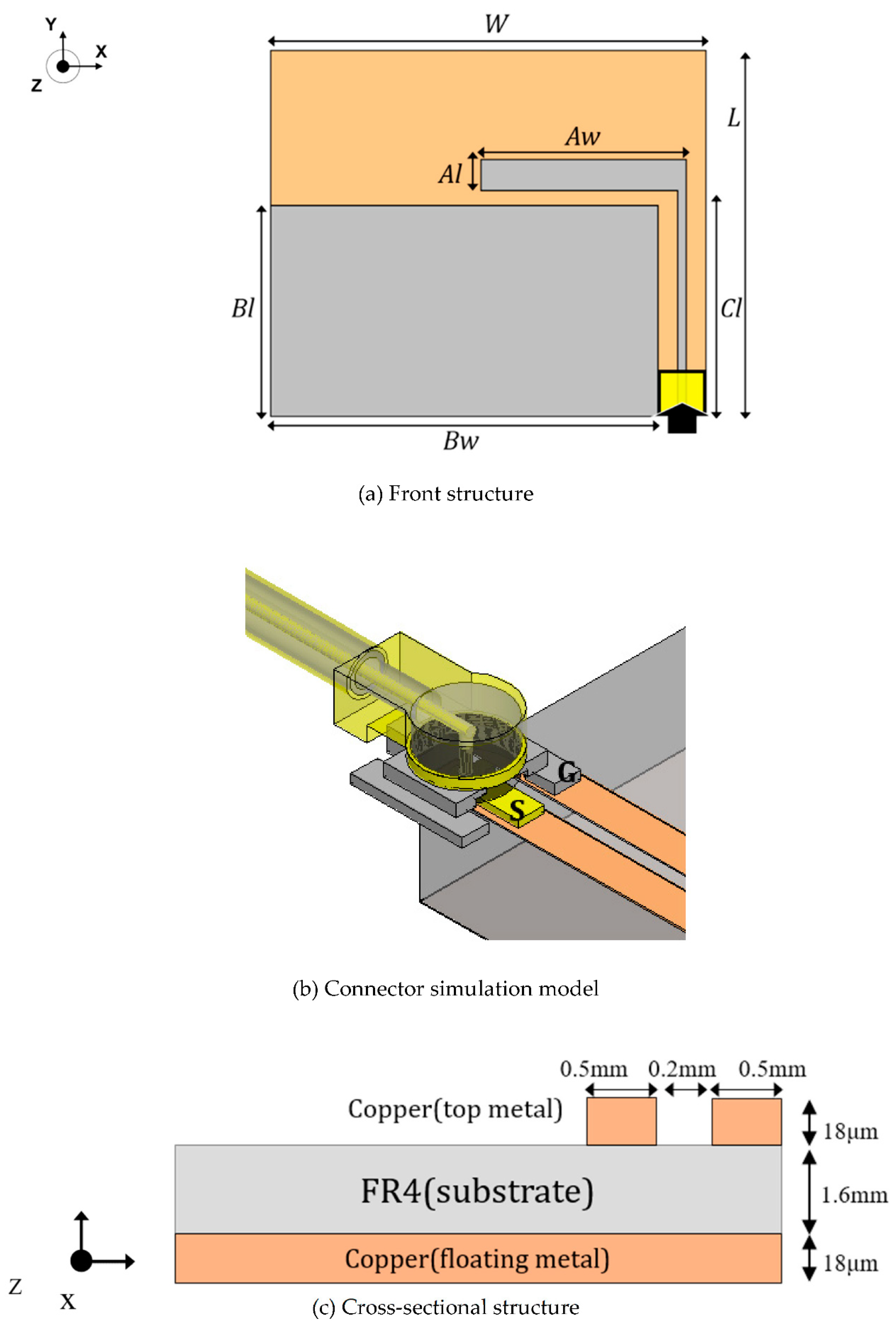
Figure 1a shows the front structure of the antenna element. The L-shaped slot extending from the feeding point in the +y and −x directions was the radiation source, and the guide wavelength was used for the design of the L-shaped slot. At an operating frequency of 9.0 GHz, the vacuum wavelength was λ_
0 = 33.3 mm, and the dielectric constant of the dielectric was ε_
r = 4.4. Therefore, the guide wavelength was λ
_g ≅ 15.9 mm when the wavelength-shortening rate was 0.48. The slot length was set to λ
_g, and the length was adjusted while confirming the resonance frequency from the simulation results. Other board size and slit size design parameters were used for impedance matching. The parameters adjusted in designing the antenna element were L, W, Al, Aw, Bl, Bw, and Cl. The design values of the adjusted parameters were as follows: L = 9.65 mm, W = 11.6 mm, Al = 0.8 mm, Aw = 5.45 mm, Bl = 5.55 mm, Bw = 10.3 mm, and Cl = 5.95 mm. By placing AW and Cl at 90°, vertical and horizontal polarizations are generated. Since Cl is a half-wavelength, Cl and AW are 90° out of phase. Therefore, a circularly polarized wave is produced.
Figure 1b shows a simulation model of the connector. The connector used was a board-mounted co-axial connector manufactured by Murata Manufacturing Co., Ltd., Kyoto, Japan, (MM5829-2700). The antenna element produced a signal on the +x-side metal of the feeding point, and the −x-side metal was the ground. The connector was mounted onto the surface of both metals by soldering.
Figure 1c shows the cross-sectional structure of the antenna element. The proposed antenna exhibited a three-layer structure, in which copper foil was attached to the front and back of FR4 (ε_r = 4.4, tan δ = 0.02). The back metal was not connected electrically to the front metal, and the connector directly contributed to radiation as it was surface-mounted. The connector was attached to reflect the back radiation of the slot antenna and obtain a high gain in the frontal direction (this is known as floating metal). The back metal of the patch antenna served as the ground, and a board thickness of λ/4 relative to the operating frequency was required for the radiation mechanism. However, the slot antenna imposed a slight effect on the characteristics of the slot antenna, and its weight could be reduced. The floating metal was attached to the back of the slot antenna, and we attempted to achieve a lightweight yet high-gain antenna.
2.2. Electric Field Distribution
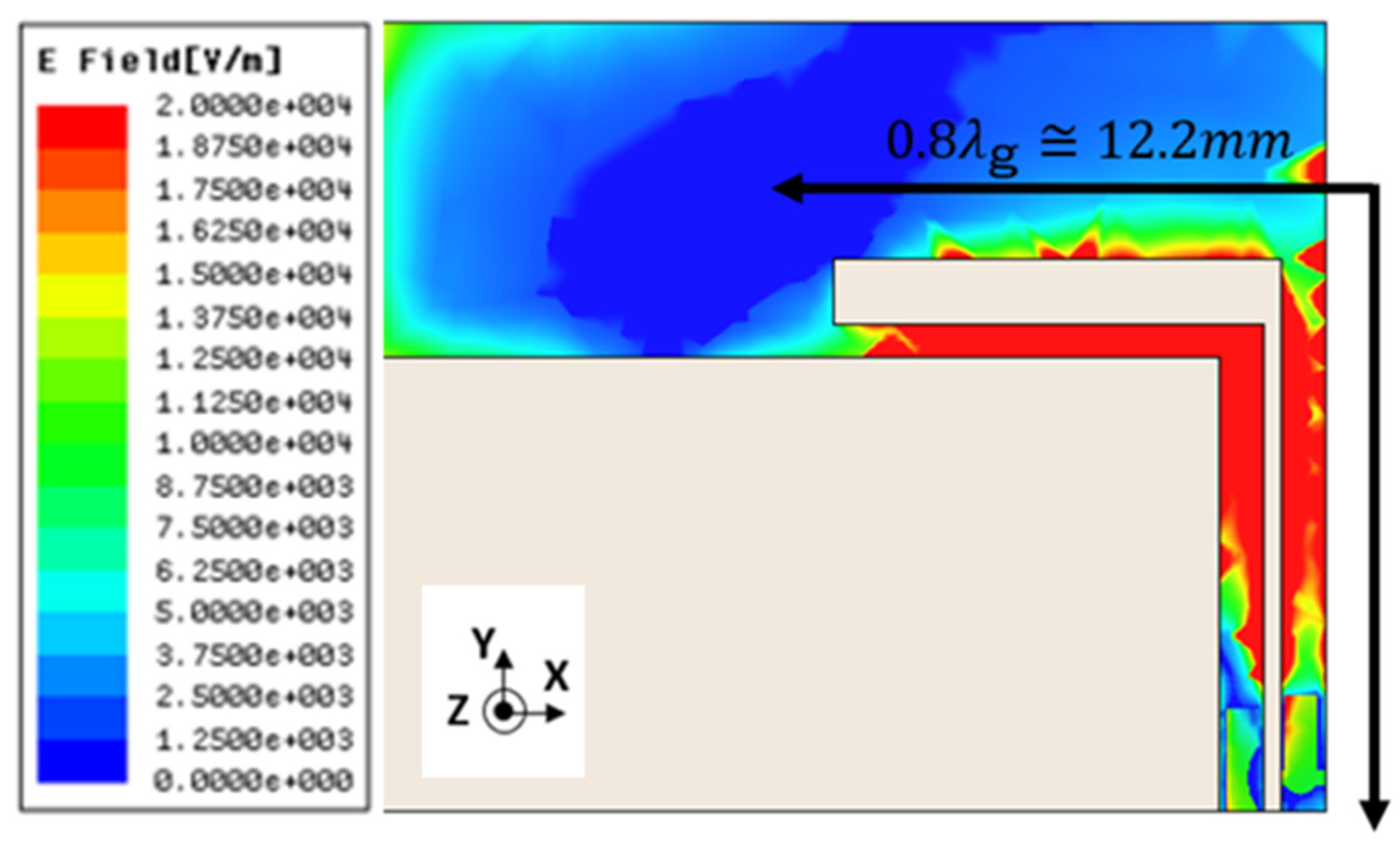
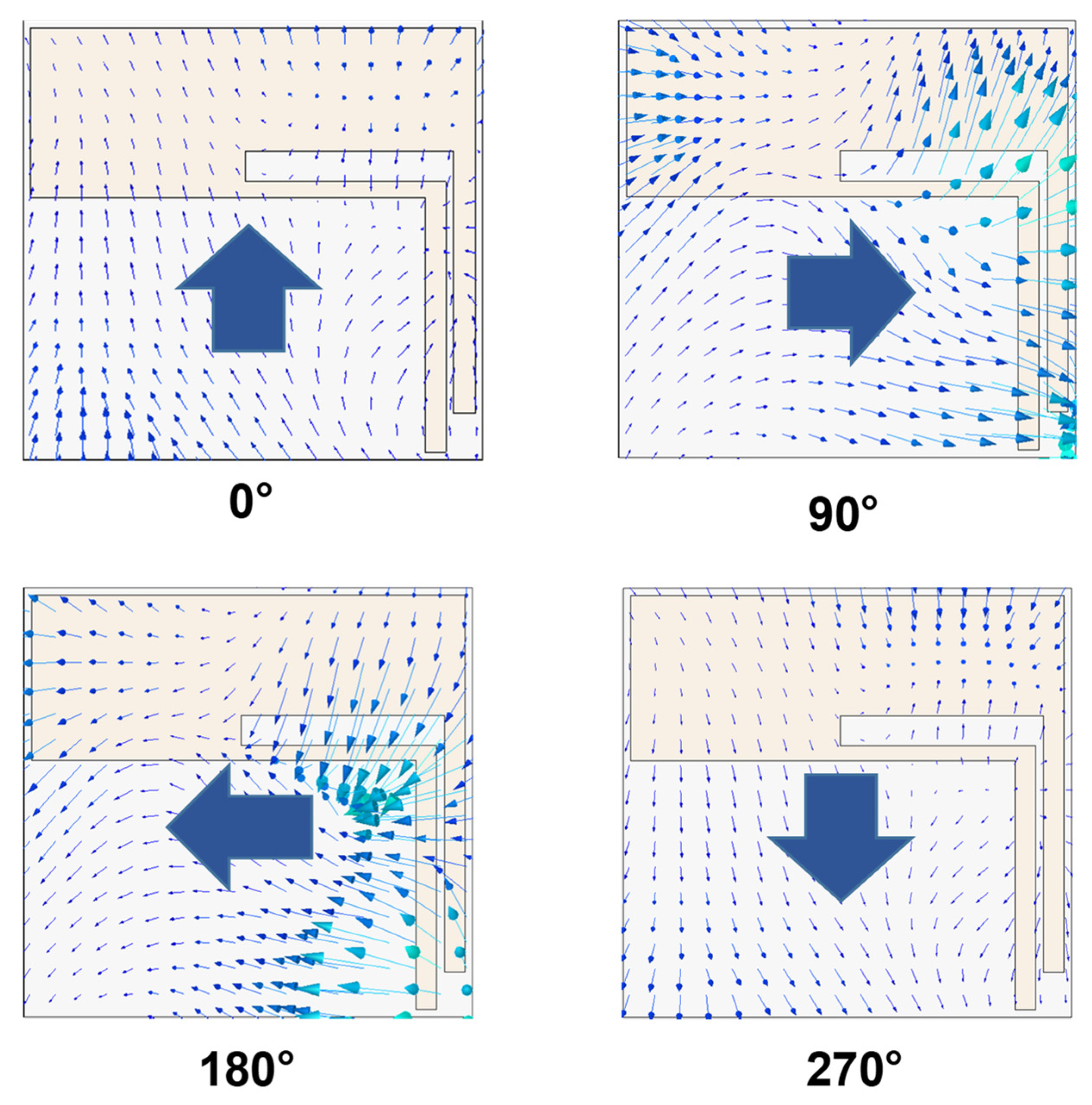
Figure 2 shows the electric field distribution of the surface metal in the antenna element. A strong electric field distribution can be confirmed in the figure from the feeding point along the L-shaped slot. The radiation mechanism can be explained by assuming a magnetic flow for the slot antenna, whereas the radiation of circularly polarized waves can be explained by assuming magnetic flow sources along the L-shaped slot in the proposed antenna. In this antenna, an electric field is generated from the feeding point to the slot section extending in the +y direction, i.e., in the x-axis direction from the magnetic flow, and from the slot section extending in the −x direction to the y-axis direction. These two forms of radiation change the directions of their electric fields to the opposite direction as the phase of the input power changes. By adjusting the phase difference of the resonance to π/2 for these two radiation sources, the polarization plane of the composite wave rotates to be consistent with the phase change, and circularly polarized waves can be confirmed.
Figure 3 shows the electric field strength distribution at 9.0 GHz in the distant field of the antenna element. It can be confirmed that the direction of the electric field vectors changes in a rotating manner as the phase of the input power changes. This signifies that the circularly polarized waves are radiating in the +z direction, in which the radio waves propagate. For the proposed antenna, it can be concluded that left-handed circular polarization (LHCP) occurs in the frontal direction when the electric field distribution is changing in the counterclockwise direction (as observed from the −z direction). Right-handed circular polarization (RHCP), which is equivalent to the frontal direction, is typically observed in the back direction. However, since the antenna was loaded with a floating metal on the back, RHCP was suppressed.
2.3. Prototype Antenna
The antenna element was prototyped using the board manufacturing and mounting service of P-ban.com Corp.
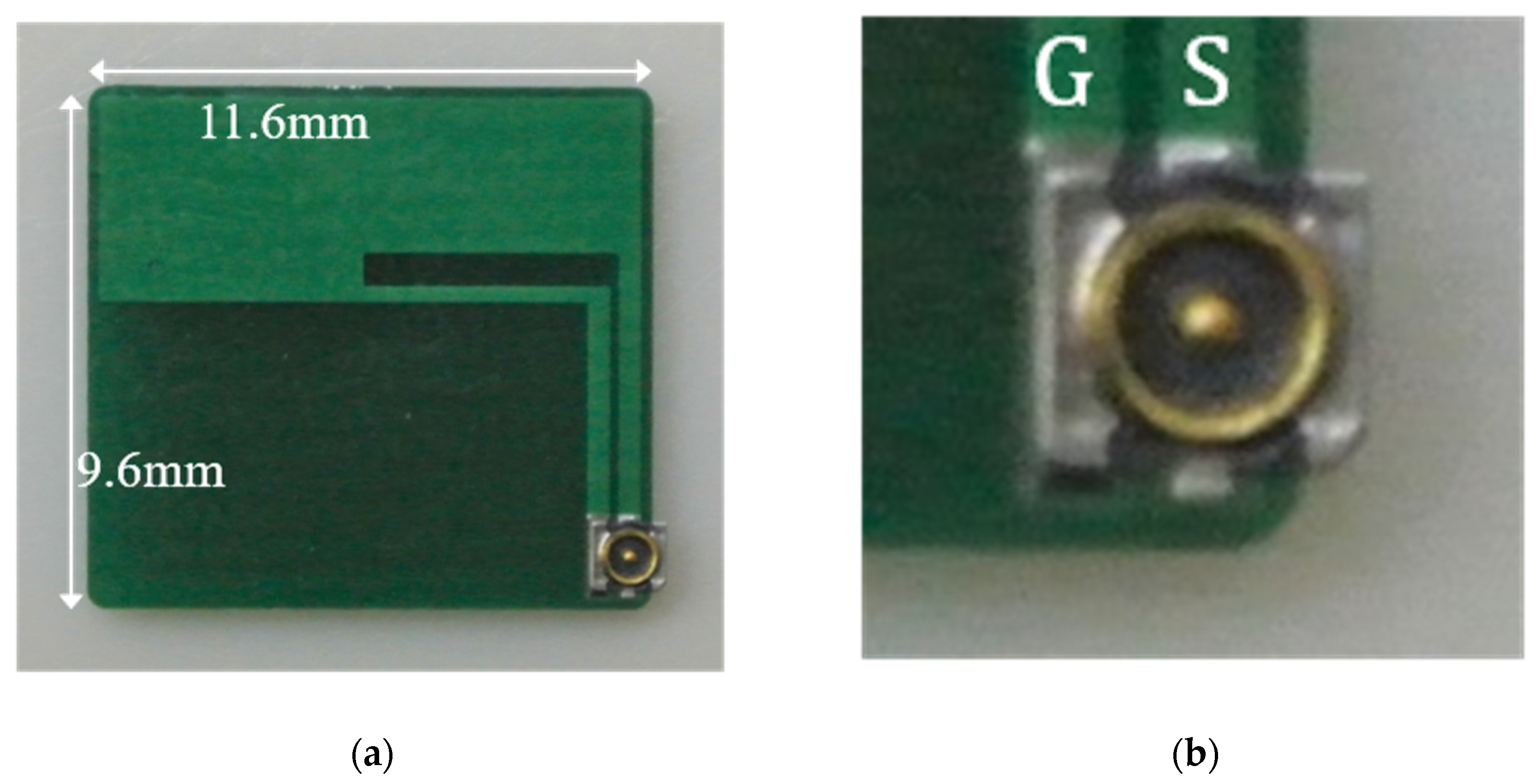
Figure 4a shows a front photograph of the prototype board. The board surface was surface-treated with a lead-free solder leveler (which is RoHS-compliant), and a green solder-resist mask was applied to both sides. The board material was FR4 with a thickness of 1.6 mm, and the copper foil pattern measured 18 μm in thickness.
Figure 4b shows an enlarged view of the connector part. The connector was a board-mounted co-axial connector manufactured by Murata Manufacturing Co., Ltd. (MM5829-2700) and was used in the simulation model. In the connector, the central pin provided the signal, and the outer two pins were grounds. As such, they were attached to the antenna element such that the left ground and central signal adhered to each other.
2.4. Simulation and Measurement Results
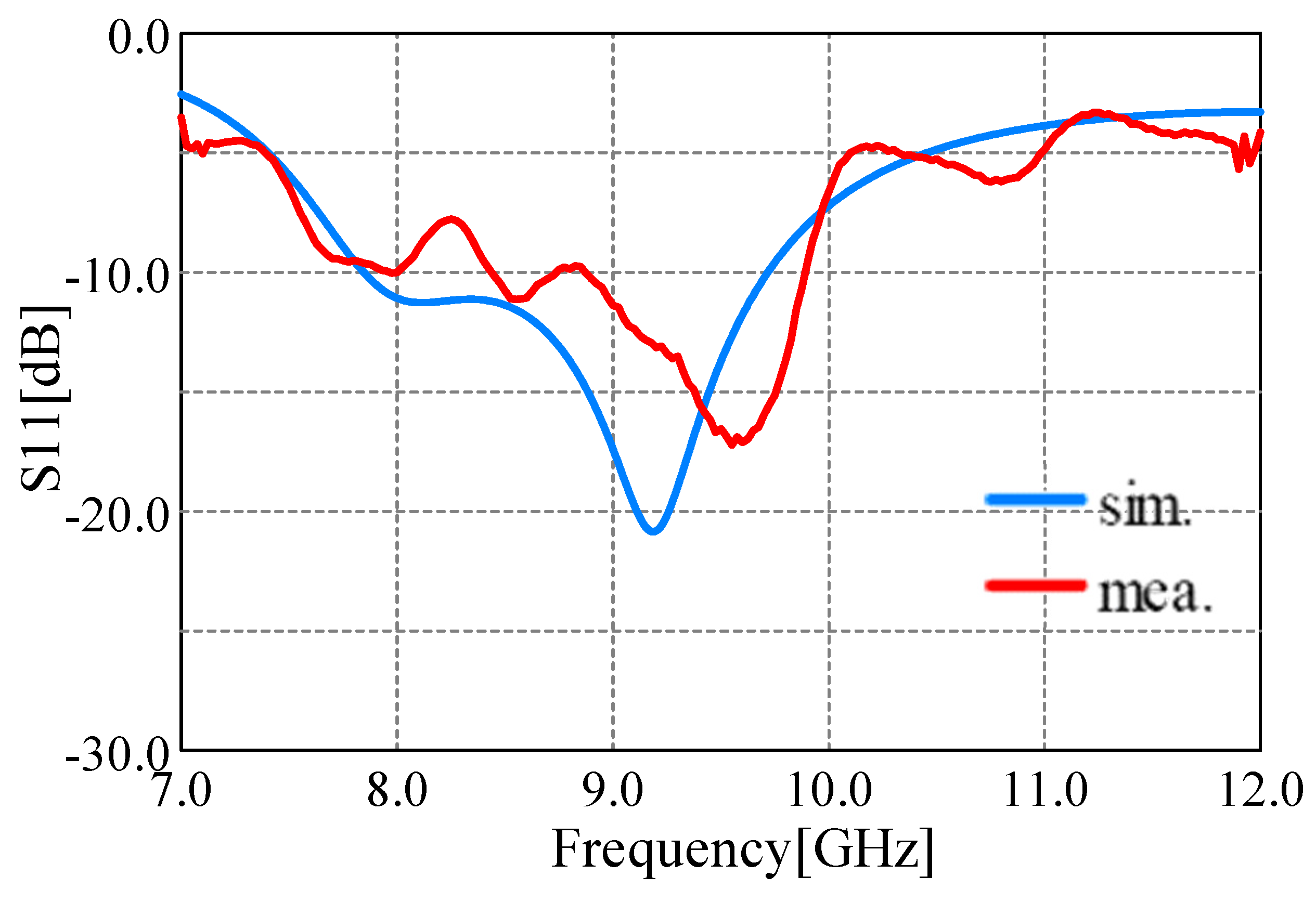
Figure 5 shows the simulation and measurement results of the S11 characteristics. The simulation results show that the resonance frequency was 9.10 GHz, and the S_11 < −10 dB band was satisfied in the 1.90 GHz range from 7.82 to 9.72 GHz. Moreover, the S_11 < −10 dB band was satisfied in the 1.04 GHz range from 8.88 to 9.92 GHz.
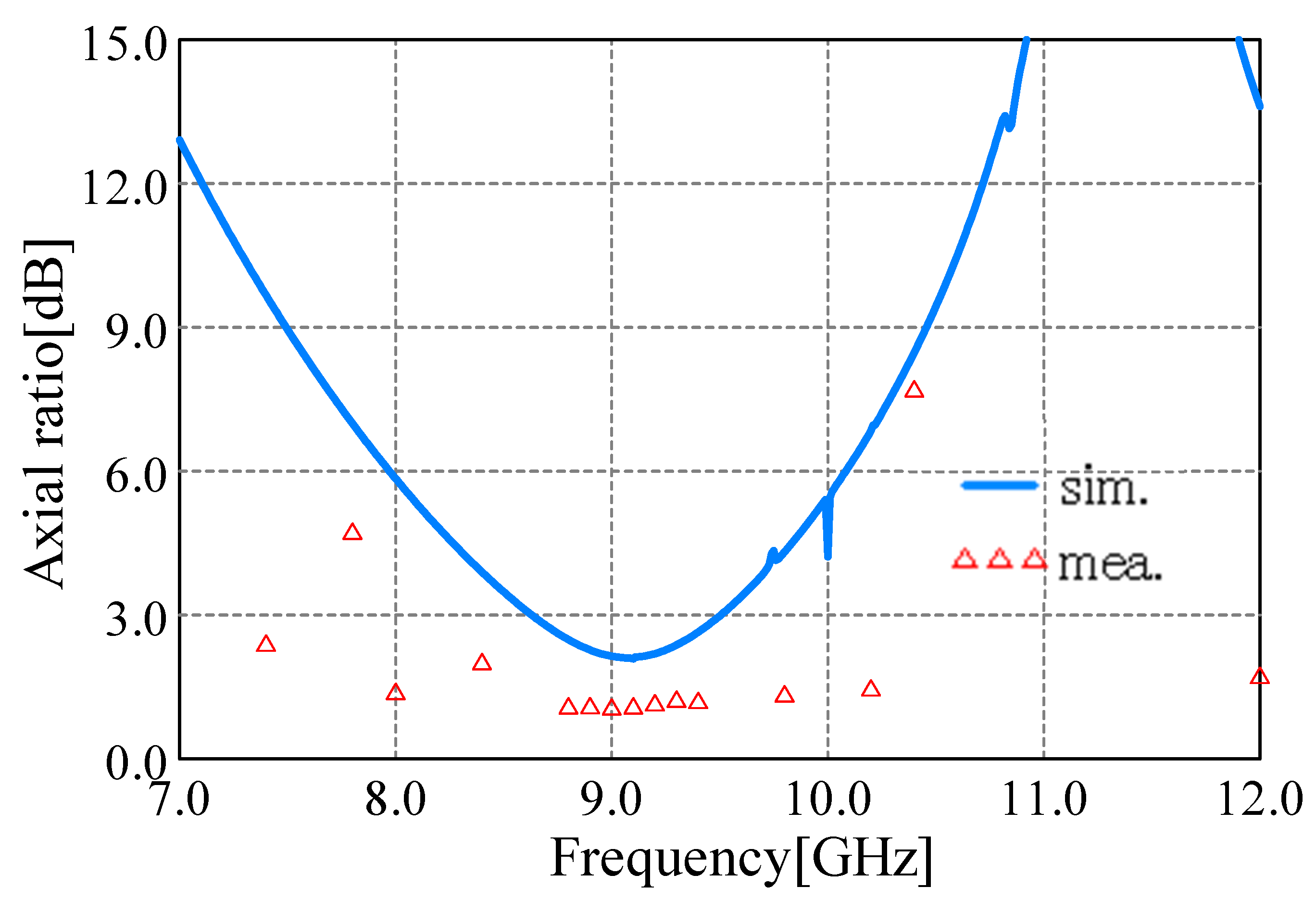
Figure 6 shows the simulation and measurement results for the axial ratio characteristics. The simulation results show that the axial ratio (AR) < 3 dB band was satisfied in the 1.09 GHz range from 8.54 to 9.65 GHz. The measurements obtained at 15 frequencies from 7.4 to 10.2 GHz were similar and satisfied the simulation results for the AR < 3 dB band. In the experiment, we measured the gain in the vertical polarization and the horizontal polarization and took the difference. In the part of
Figure 6 where the gain is high, the AR is smaller, so good circular polarization is generated, which is better than the design value. On the other hand, where the gain is small in
Figure 6, the received power for the vertical and horizontal polarization is small, so a difference is created in the noise, and thus the SN of the low-gain area is poor and may not match the design value.
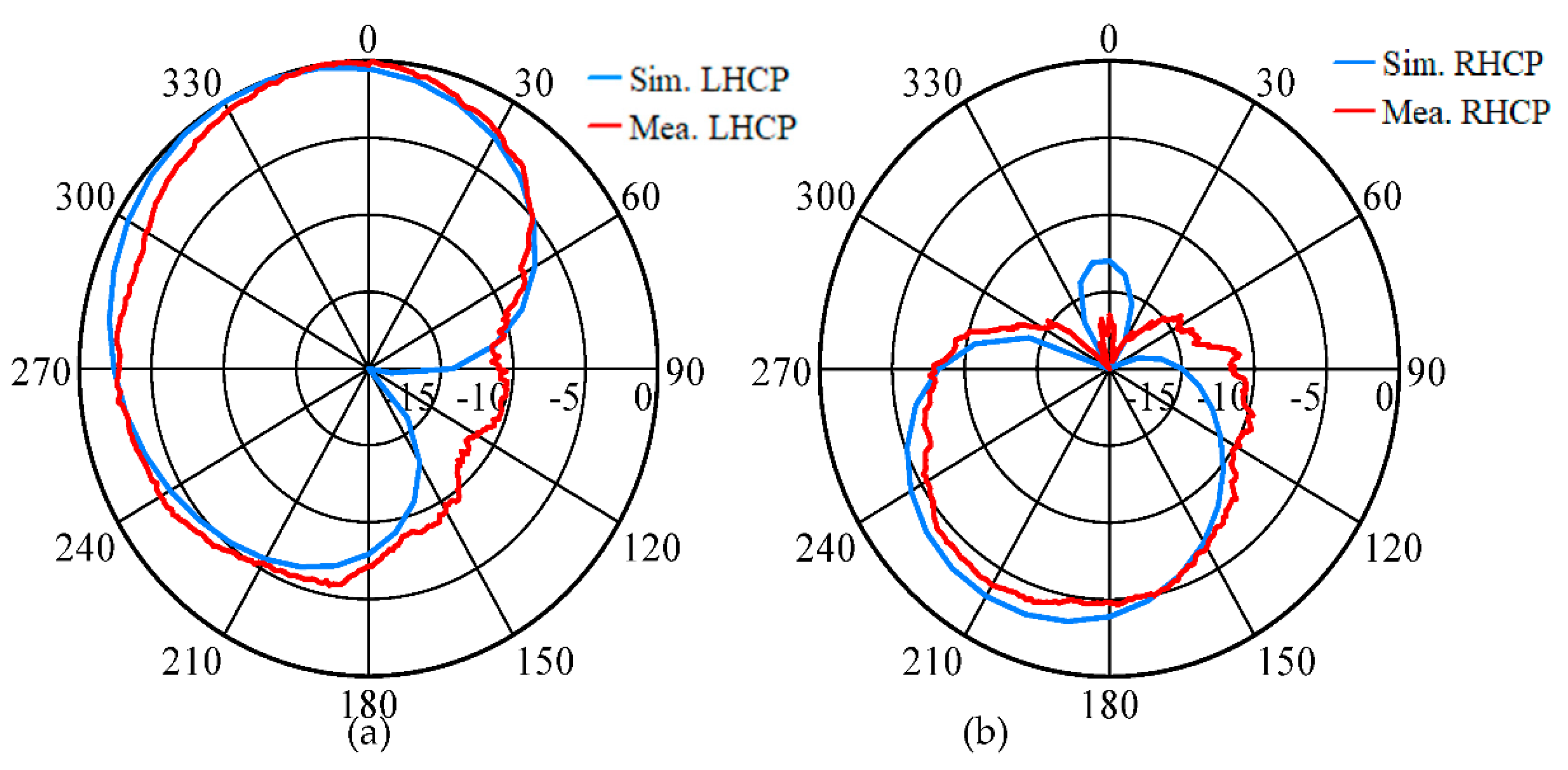
Figure 7 shows the simulation and measurement results for the radiation pattern. The radiation patterns for the LHCP and RHCP are each shown in the xz-plane. Furthermore, the simulation and measurement values were standardized to compare them with the measurement results. For the LHCP, the simulation results exhibit a half-width of 112° and a front–back (FB) ratio of 13.2 dB, whereas the measurement results exhibited a half-width of 110° and an FB ratio of 10.8 dB.
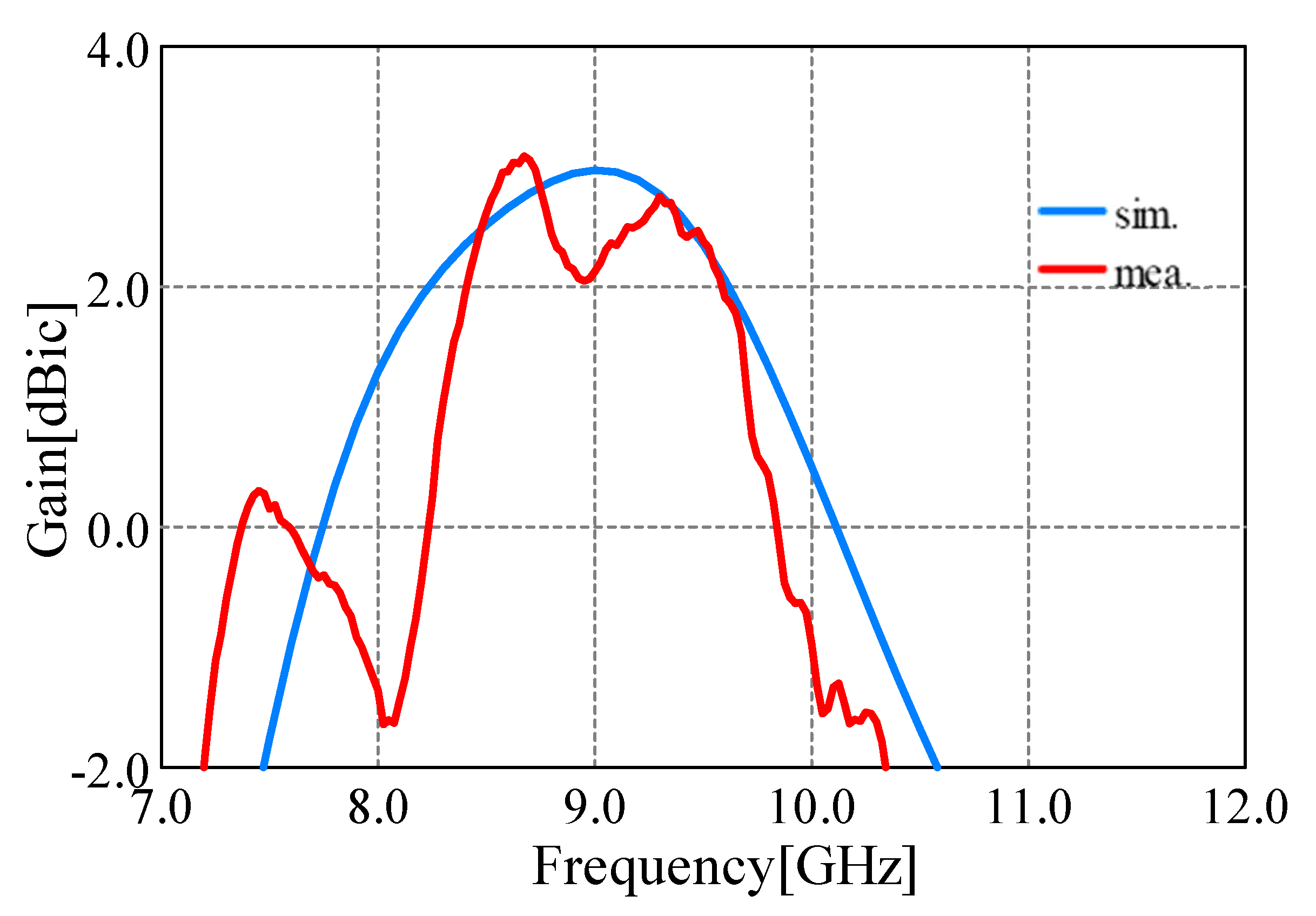
Figure 8 shows the measurement and simulation results for the frequency characteristics. The maximum gain in the simulation results was 3.3 dBic @ 9.02 GHz, and the 3-dB gain-band was 2.43 GHz (7.74–10.17 GHz). The maximum gain in the measurement results was 3.04 dBic @ 8.83 GHz, and the 3-dB gain-band was 1.63 GHz (8.23–9.86 GHz).
2.5. Discussion
In this subsection, we discuss the simulation and measurement results for an antenna element. The simulation results for the reflection characteristics indicate a resonance frequency of 9.10 GHz, whereas the measurement results indicate 9.62 GHz. This deviation is attributable to errors in the board permittivity. In the design model of the antenna, the permittivity of the board FR4 was fixed to ε_r = 4.4 for the simulation. However, the permittivity decreased during operation in the high-frequency band, and it was assumed that, consequently, the resonance frequency shifted to a higher range. Therefore, we plan to consider errors in board permittivity in future designs.
Regarding the gain frequency characteristics, the simulation results show a maximum value at a central frequency of approximately 9.0 GHz, whereas the measurement results show a partial decrease. This deviation is attributable to the bonded part of the connector. In the antenna element, only one of the two grounds in the connector was used. Therefore, the other released ground may affect the characteristics. Alternatively, errors might have occurred in the measurement environment or when fabricating the board.
The simulation results for the gain frequency characteristics show a maximum gain that was in a range lower than that for the resonance frequency. Therefore, we designed the antenna by shifting the resonance frequency from the target frequency to obtain the maximum gain. Results that were more favorable than the simulation results were obtained at all frequencies in terms of the axial ratio characteristics. Hence, the design above is regarded as the most favorable.
The simulation results for the radiation pattern show that the LHCP and RHCP radiated in the +z and −z directions, respectively. However, strong radiation was observed in the LHCP. As such, the high gain in the floating metal was confirmed. A large half-value angle was obtained for the radiation pattern of the LHCP. However, it was demonstrated that further gain increases can be obtained by sharpening the beam using an array.
3. Array Antenna
In this section, an array for the above-mentioned antenna element is analyzed based on the structures of the slot antennas and feedlines. In each subsection, we present the design models and results for the feedlines and 2 × 2 array antenna.
3.1. Structure
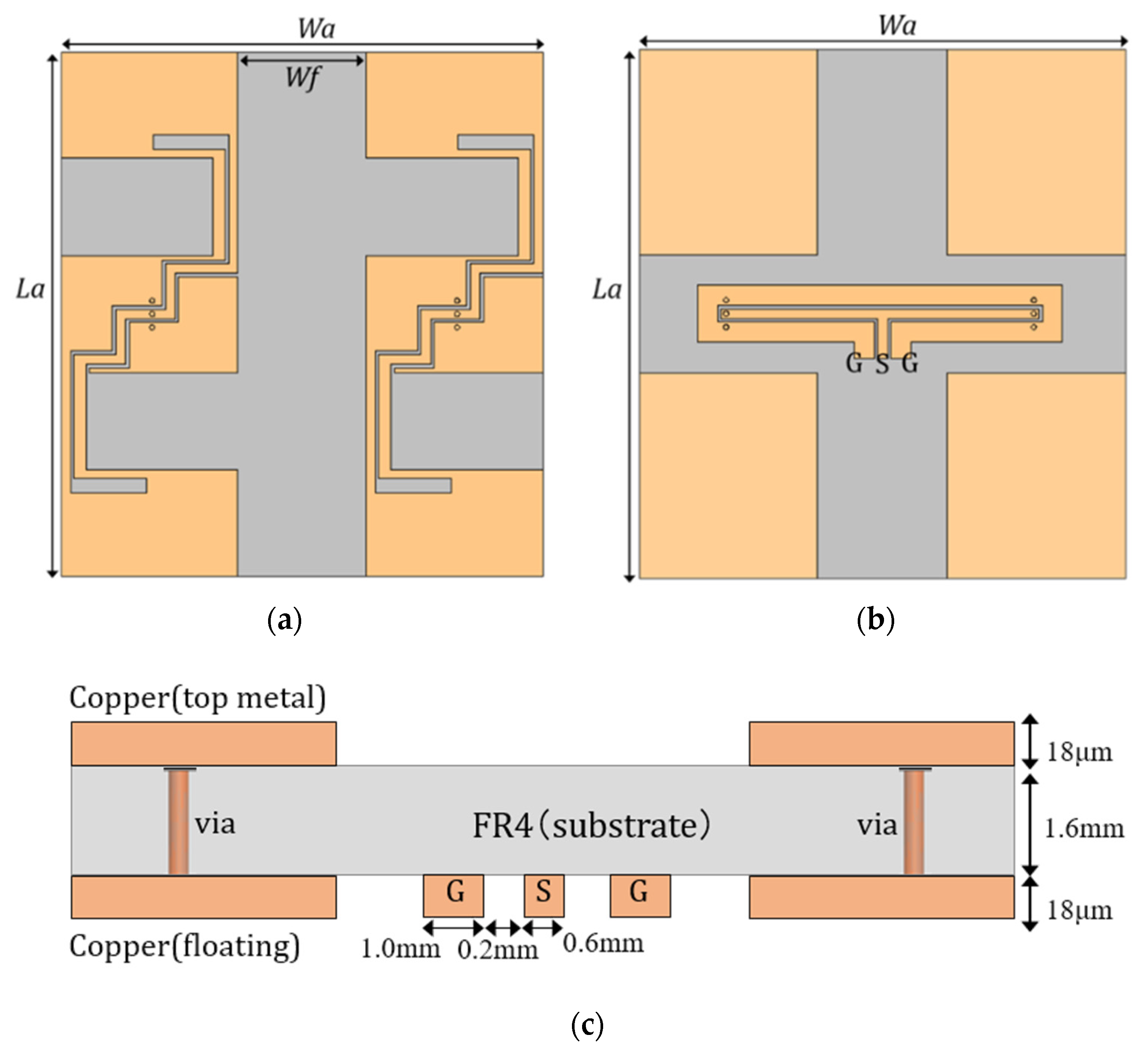
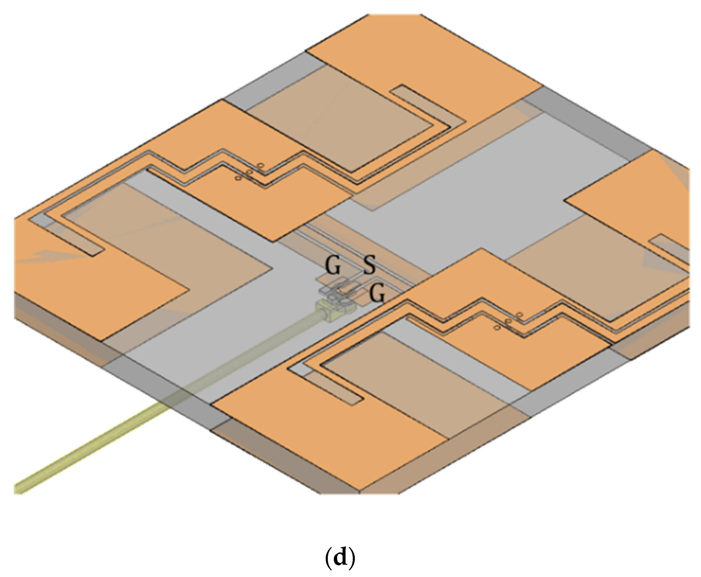
Figure 9 shows the structure of the proposed 2 × 2 array antenna. The feeding point was the one-port of the back co-planar branch line. The back co-planar branch line was connected by the same ground signal as the front co-planar line, and power was supplied to the two antenna elements arranged in the ±x direction.
The design parameters were adjusted and impedance matching was conducted to adjust the operating frequency of the array antenna. The adjusted design parameters were W, L, Bl, Bw, Cl, Al, and Aw. The final design values of the parameters were as follows: Wa = 29.2 mm, Wf = 7.8 mm, La= 31.7 mm, W = 10.7 mm, L = 12.3 mm, Bl = 5.9 mm, Bw = 9.2 mm, and Cl = 6.4 mm.
3.2. Prototype Antenna
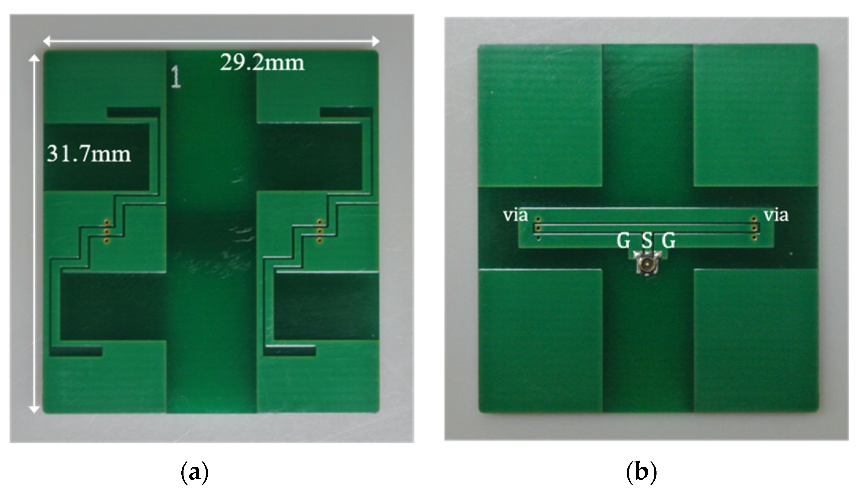
Figure 10 shows a photograph of the 2 × 2 array antenna board. The board manufacturing and mounting service of P-ban.com Corp was used for the prototype. The board surface was surface treated with a lead-free solder leveler (which is RoHS-compliant). The connector was bonded to the back co-planar feedline with the aligned ground signal. The via connecting the back and front surface co-planar lines had a via diameter of 3.0 mm and a land diameter of 6.0 mm. The final antenna had the following dimensions: 29.2 mm × 31.7 mm, thickness = 1.636 mm.
3.3. Simulation and Measurement Results
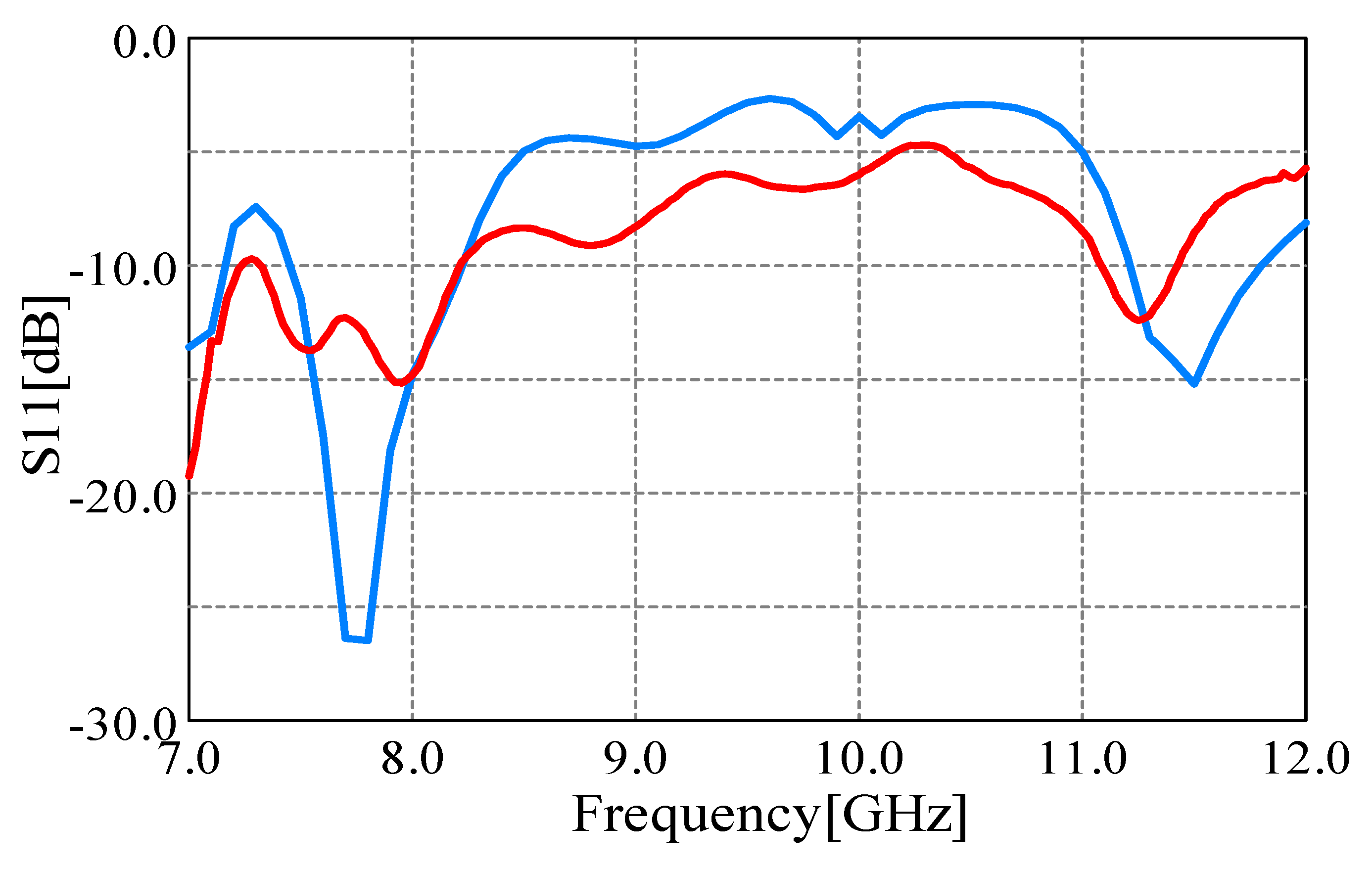
Figure 11 shows the simulation and measurement results for the reflection characteristics. It was confirmed that the resonance frequencies of the simulation and measurement results were almost identical in the 9.0 GHz band.
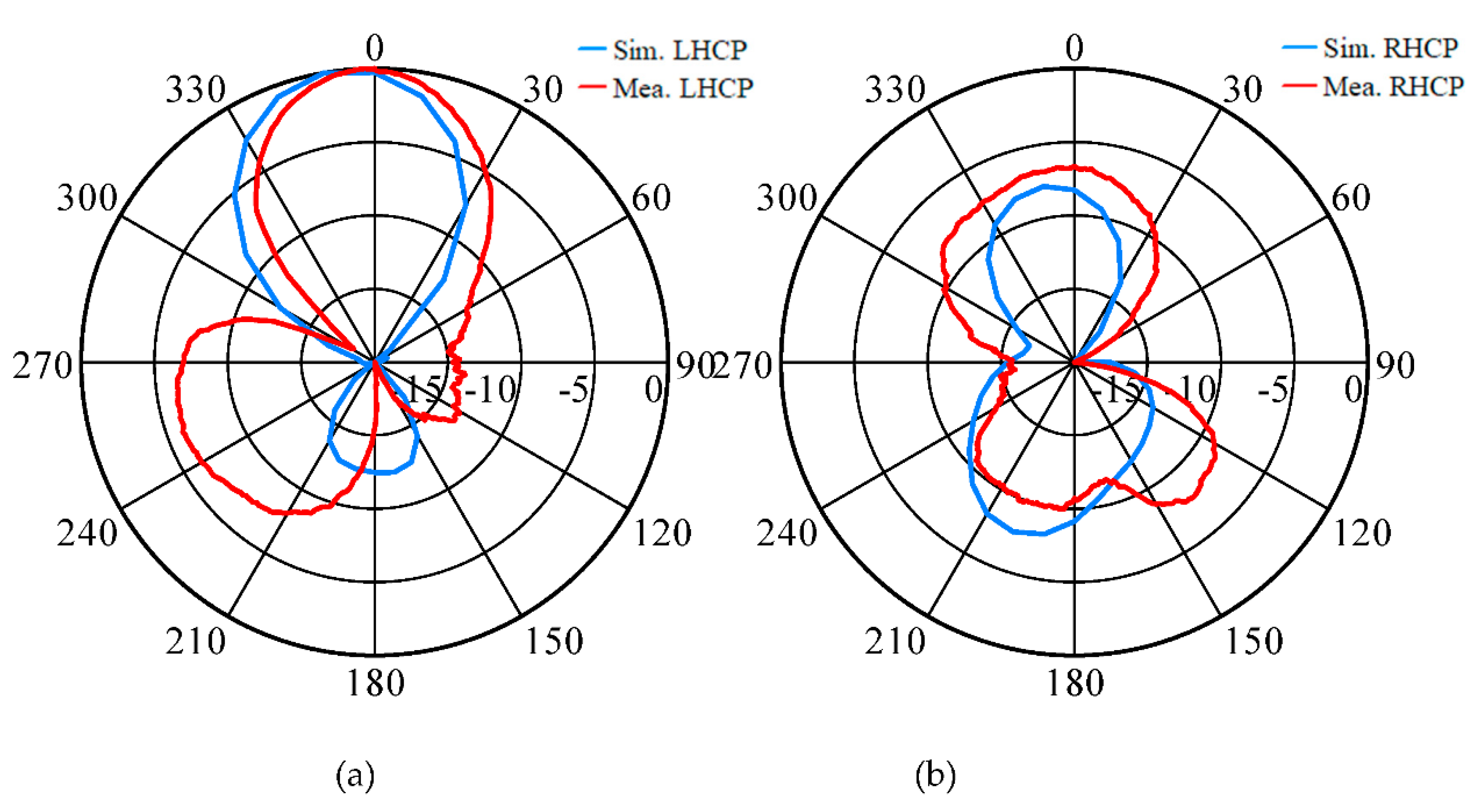
Figure 12 shows the measurement and simulation results for the radiation pattern. The radiation patterns for the LHCP and RHCP are each shown in the xz-plane. We can clearly see that the gain of the LHCP is larger than that of RHCP. This result shows the prototype antenna is the LHCP antenna. For the LHCP, the simulation results show a half-value width of 42° and an FB ratio of 17.4 dB, and the measurement results show a half-value width of 44° and an FB ratio of 12.4 dB.
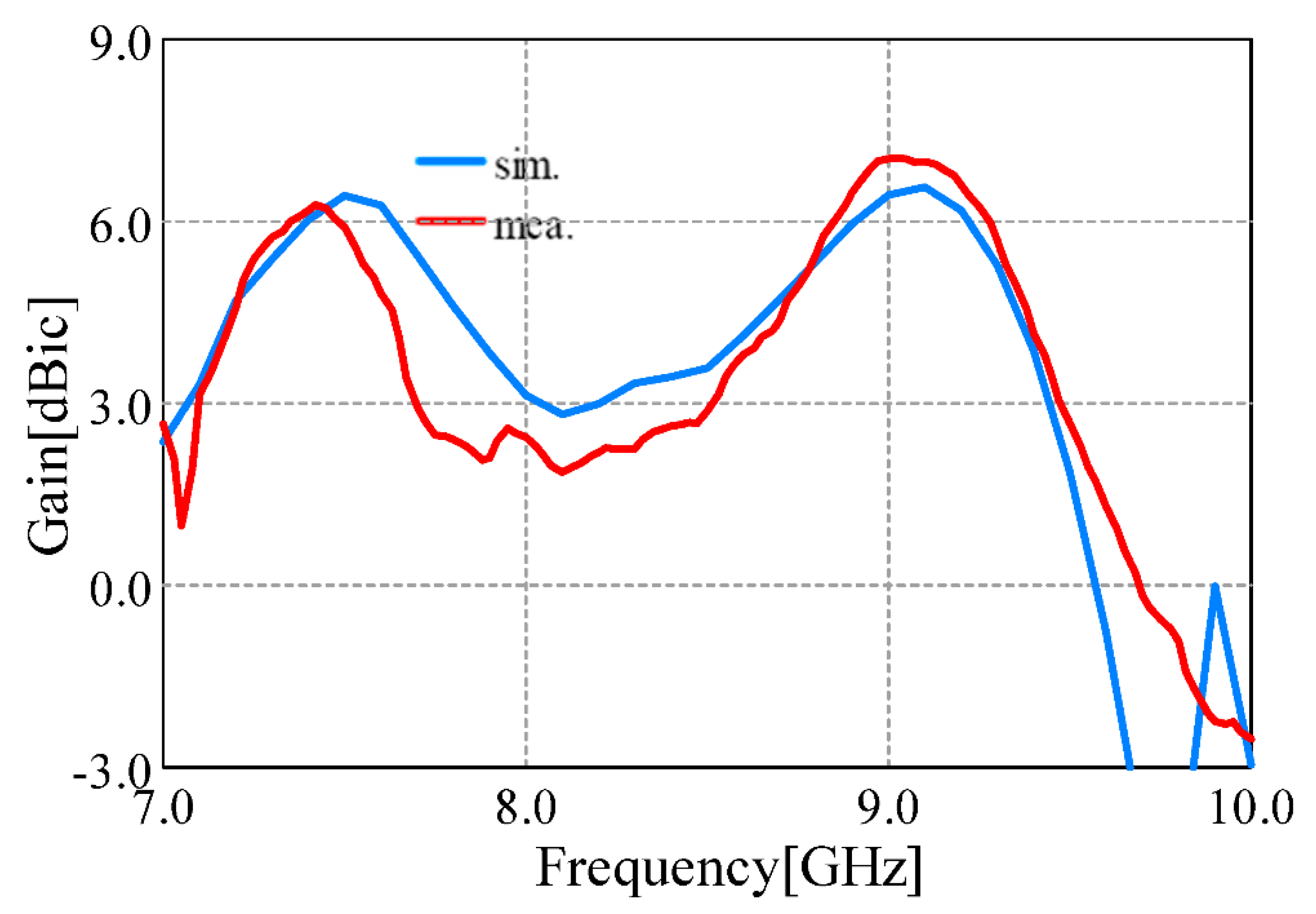
Figure 13 shows the measurement and simulation results for the gain frequency characteristics. The simulation results show a maximum gain of 6.42 dBic @ 9.12 GHz, and the 3-dB gain-band was 1.04 GHz (8.34–9.38 GHz). The measurement results show a maximum gain of 6.94 dBic @ 9.02 GHz, and the 3-dB gain-band was 900 MHz (8.55–9.45 GHz). The maximum gain of the array antenna exhibited an increase of 3.38 dBic compared with that of the antenna element.
Next, in
Table 1, the proposed antenna was compared with other reported antennas [
19,
20,
21,
22,
23,
24]. The proposed technique based on the slot antenna structure has a distinct advantage over other state-of-the-art designs in the context of antenna thickness. The antenna characteristics qualify the antenna to be used in UWB applications.
3.4. Discussion
The simulation and measurement results for the radiation pattern indicate sharp beam radiation due to the front-oriented array in the xz-plane of the LHCP. Compared with the beam width of the antenna element, that of the array antenna decreased by 70°, but a higher gain was obtained. Unlike the LHCP, the RHCP enabled the radiation to be suppressed to a small amount. In addition, it was confirmed that the floating metal functioned in the array antenna. The measurement results for the radiation pattern in the LHCP show strong radiation in the 240° direction, which was not reflected in the simulation results. One reason for this was the effect of the co-axial cable being connected to the antenna when the radiation patterns were measured.
The measurement and simulation results for the gain–frequency characteristics show that their peak frequencies were identical. However, when compared with the simulation results, a gain decrease of approximately 1 dB was observed in some frequency bands, and this was assumed to be due to the measurement environment and errors during board construction.


