Article

CMOS Interface Circuits for High-Voltage Automotive Signals

1
Department of Engineering and Architecture, University of Parma, 43124 Parma, Italy
2
Silis S.r.l., 43121 Parma, Italy
*
Author to whom correspondence should be addressed.
Electronics 2022, 11(6), 971; https://doi.org/10.3390/electronics11060971
Submission received: 21 February 2022 / Revised: 16 March 2022 / Accepted: 18 March 2022 / Published: 21 March 2022

Abstract

:
The acquisition of high-voltage signals from sensors and actuators in an internal-combustion engine is often required for diagnostic purposes or in the case of conversion to alternative fuels, such as hydrogen, natural gas, or biogas. The integration of electronic interfaces and acquisition circuits in a single device provides benefits in terms of component-count reduction and performance. Nonetheless, the high voltage level of the involved signals makes on-chip design challenging. Additionally, the circuits should be compatible with the CMOS technology, with limited use of high-voltage options and a minimum number of off-chip components. This paper describes the design and the implementation in 350 nm CMOS technology of electronic interfaces and acquisition circuits for typical high-voltage signals of automotive context. In particular, a novel co-design of dedicated voltage clamps with electro-static discharge (ESD) protections is described. The proposed circuits require only a single off-chip resistor, and they are suitable for the acquisition of signals with peak voltages up to 400 V. The measured performance of the silicon prototypes, in the [−40 °C, +125 °C] temperature range, make the proposed electronic interfaces suitable for the automotive domain.

1. Introduction

Under the hood of a car, several sensors and actuators operate to support the control of the internal-combustion engine. Indeed, parameters such as fuel-injection start time and duration, ignition instants, and engine rotation speed are critical for optimizing the performance in terms of fuel consumption and power. The electronic control unit (ECU), the core of the engine control systems, acquires signals from external sensors, and drives the actuators in the car engine [1,2,3,4].
In recent decades, there has been significant interest for the conversion of spark-ignited internal-combustion engines from gasoline to compressed natural gas (CNG), liquefied petroleum gas (LPG), biogas, or hydrogen [5,6,7,8,9]. Additionally, the conversion of compression-ignited engines from a single fuel (i.e., diesel) to a mixture of diesel and gas has been investigated [10]. Despite the rapid and growing diffusion of vehicles powered by electric motors, the well-affirmed endothermic engine is still far from being completely replaced. Indeed, it will take decades to substitute the huge number of cars with traditional engines for full-electric counterparts. Moreover, the perspective of car engines for the next generation remains uncertain. Indeed, natural gas remains an attractive alternative to liquid fossil fuels, providing benefits in terms of emissions in specific contexts [11,12]. In recent years, the interest for the hydrogen as car fuel has grown [13,14], which can give a new boost to endothermic engines [15,16]. Examples of conversion in internal-combustion engines from gasoline or diesel to hydrogen are reported in [7,17,18].
The conversion of an internal-combustion engine to gas requires, among other things, an additional ECU (gas-ECU) that acquires signals from some actuators and sensors, and communicates with the main ECU. The gas-ECU is mandatory to properly drive the dedicated gas injectors and adapt the engine control parameters to the properties of the alternative fuel. Typical gas-ECU inputs are the high-voltage signals at the igniter coil and the differential output signal of the inductive sensor to measure the speed of the engine crankshaft. In the engine conversion to dual-fuel (i.e., diesel and CNG or diesel and hydrogen), the diesel injectors are monitored to limit the fuel quantity to the minimum value required to guarantee gas ignition [19,20]. Thus, the voltage signals at the low and high sides are useful for this purpose. Furthermore, in single-fuel engines, a readout of injector signals is often required for diagnosis purposes [21]. The design of the circuit interface and readout is challenging, since those signals exhibit peak values largely exceeding the regulated supply voltage of the readout of electronic circuits and the maximum input voltage that the involved devices can tolerate before incurring permanent damage. Therefore, additional protections are added to the circuits in the ECU board to clamp the input signal below a safe value and to protect the front-end circuits. However, such additional off-chip devices increase the cost of the ECU, the component count, and the printed circuit board (PCB) area. Other issues occur if the circuit is designed to detect a voltage step with both the low and the high level exceeding the rated input voltage of the input device. In this case, a simple voltage clamp, either off-chip or on-chip, cannot be used, since it would remove the relevant signal transition from the input signal.
Protection against the electro-static discharge (ESD) events demands particular attention. The protection strategy should rely only on on-chip clamping devices, ensuring an ESD protection level suitable for automotive applications, i.e., higher than the 2 kV human-body model (HBM). However, such ESD devices should not be activated by high-voltage input signals in order to avoid interfering with the integrated clamp that is tailored to the specific signal to be acquired.
This paper describes the design and implementation of CMOS interface circuits suitable for high-voltage automotive signals, with fully integrated clamps. The proposed circuits allow a full integration of both clamping and readout circuits in a single chip, thus minimizing the component count and the ECU cost. The prototype was implemented in 350 nm CMOS technology, including only the high-voltage option of DMOS transistors with 70 V drain-source breakdown and 5 V gate oxide.
The main novelty of the proposed interface circuits is the full integration into CMOS technology of co-designed ESD protections and over-battery voltage clamps, with 5 V gate-oxide transistors and minimum high-voltage options.
The paper is organized as follows. In Section 2, the considered automotive signals are described with the dedicated interface and acquisition circuits. In particular, the multi-level clamping technique is described with the added ESD protection devices. In Section 3, the chip prototype is described, and the measurement results are reported.

2. Automotive Signals and Readout Circuits

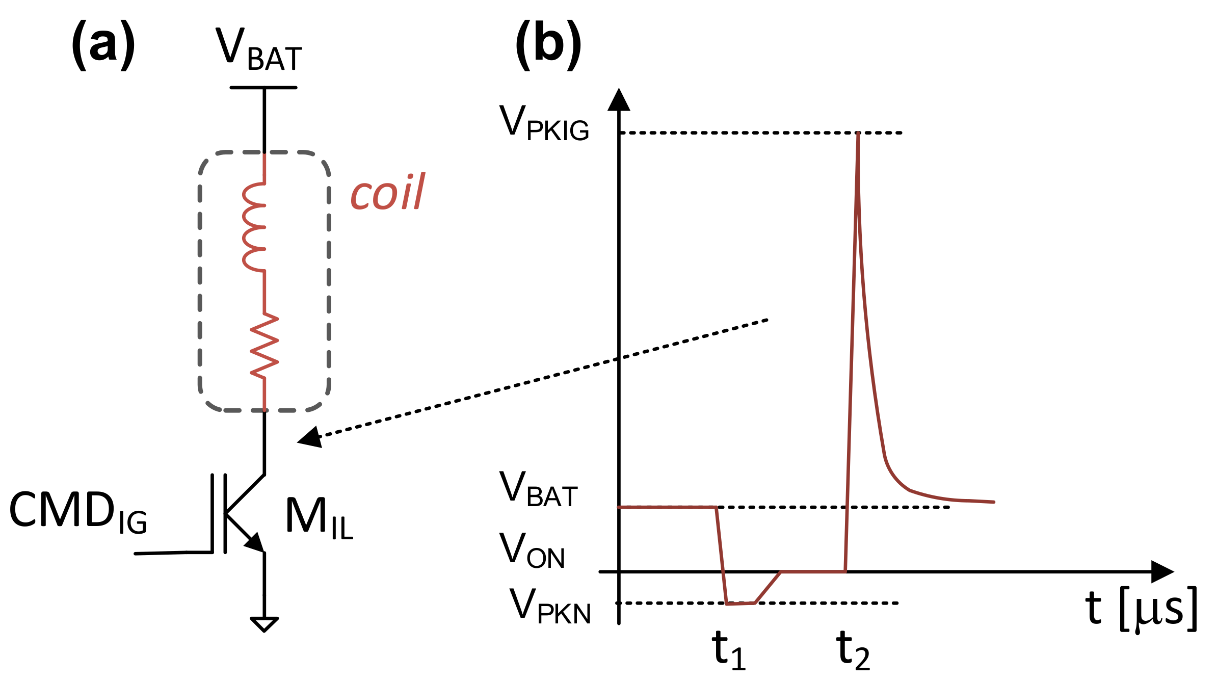
2.1. Injector and Igniter Signals

In the internal-combustion engine, the injector is an electro-magnetic valve used to dispense fuel either into the intake manifold or directly into the combustion chamber [22,23,24]. The latter case usually guarantees better power performance and lower consumption, and it corresponds to spark-ignition engines with gasoline direct injection (GDI) or diesel engines with common-rail direct injection (CRDI). A typical driving circuit for the fuel injectors in GDI or CRDI engines is shown in Figure 1a. The power-MOS transistors M H 1 and M H 2 connect the high side of the injector, modeled with an L-R equivalent, to either the battery voltage, i.e., 12 V, or to a high-voltage rail, up to approximately 80 V. The latter is locally generated by a DC–DC converter, shared among all the injectors [25,26].
This dual-voltage control increases the time derivative of the current at the onset of the injector activation with respect to the case of a single 12 V supply, leading to more accurate control of the fuel-injection startup time. The insulated-gate bipolar transistor (IGBT) M L 1 , connected to the injector low side, is used to rapidly reduce the driving current during the injection phase and at the end of the injection window. The simplified voltage waveforms at the high and low sides of the injector are shown in Figure 1b,c, respectively, while the command waveforms, i.e., C M D L 1 , C M D H 1 , and C M D H 2 , are in Figure 1d, where the high-level condition corresponds to the closed-switch state.
In the OFF phase, the low-side switch is open, and the high-side terminal of the injector is connected to the battery rail. At t A , the preliminary magnetization (PM) phase starts with M L 1 closed and the current flowing through the injector coil. The fuel injection starts at t B , when the high side is connected to the high-voltage rail and the time derivative of the input current suddenly increases, achieving a fast injector activation. Once the injector has been completely switched on, the bootstrap (BS) phase ends and the control current is reduced to limit the thermal stress of the coil. Thus, the modulation (MOD) phase occurs from t c onwards, with the injector initially disconnected from the high-voltage rail by switching off the high-side transistor. The injector modulation is implemented also at the low-side (LSMOD) by switching off M L 1 for a short time. This procedure rapidly decreases the current to the minimum level, but still maintains the injector in the ON state. Moreover, it causes the low-side voltage to abruptly rise to the clamping voltage, usually set by the protection diode of M L 1 , not included in the figure. For the remaining time of the injection window, the high side is periodically connected to the battery rail to maintain the injector current at the required level, i.e., high-side modulation (HSMOD) [27]. The injection phase terminates at t D by switching off the low-side device, causing the low-side voltage to rise again to the clamping voltage, which is typically in the 80–100 V range.
For diagnostic or control purposes the length of the high-voltage pulse at the high-side, i.e., t C t B , matters. Additionally, the functionality of the low-side switch is monitored by detecting the crossing of a threshold set at half the battery voltage measuring t A , t C , and t D . An example of measured voltage waveform at the injector high side in a GDI engine is in the plot of Figure 2a.
Another example of high-voltage signals in the automotive context is found at the low-side of the ignition coil. Indeed, each spark plug of the ignition engine requires the generation of a very high voltage. This is usually obtained, in every engine cycle, connecting a coil first between the battery rail and ground to accumulate energy, and then disconnecting it from ground, at the ignition instant [28]. The equivalent circuit is shown in Figure 3a, where the IGBT M I L implements the low-side control of the coil. At the low-to-high transition, the voltage at the IGBT collector increases up to about 400 V to successively settle to the battery voltage level [29,30]. The ignition instant, i.e., t 2 in Figure 3b, is precisely measured by detecting the crossing of the low-side coil voltage at a threshold, usually set to half the car-battery voltage, V B A T / 2 . It should be noticed that the coil inductance combined with the capacitance at the IGBT collector can lead to a negative voltage transient at the beginning of the coil pre-charge phase, i.e., t 1 , with the IGBT switched on. A measured waveform at the low side of the ignition coil is shown in Figure 2b.

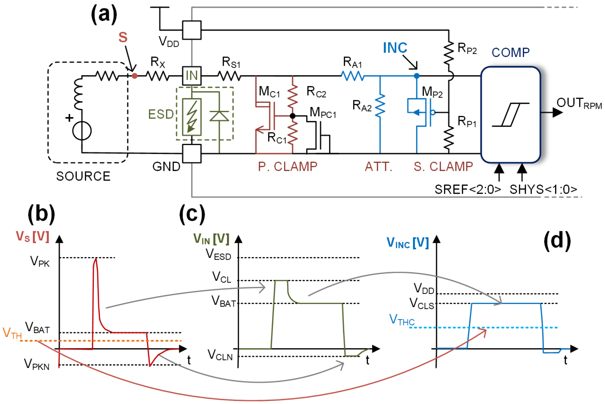
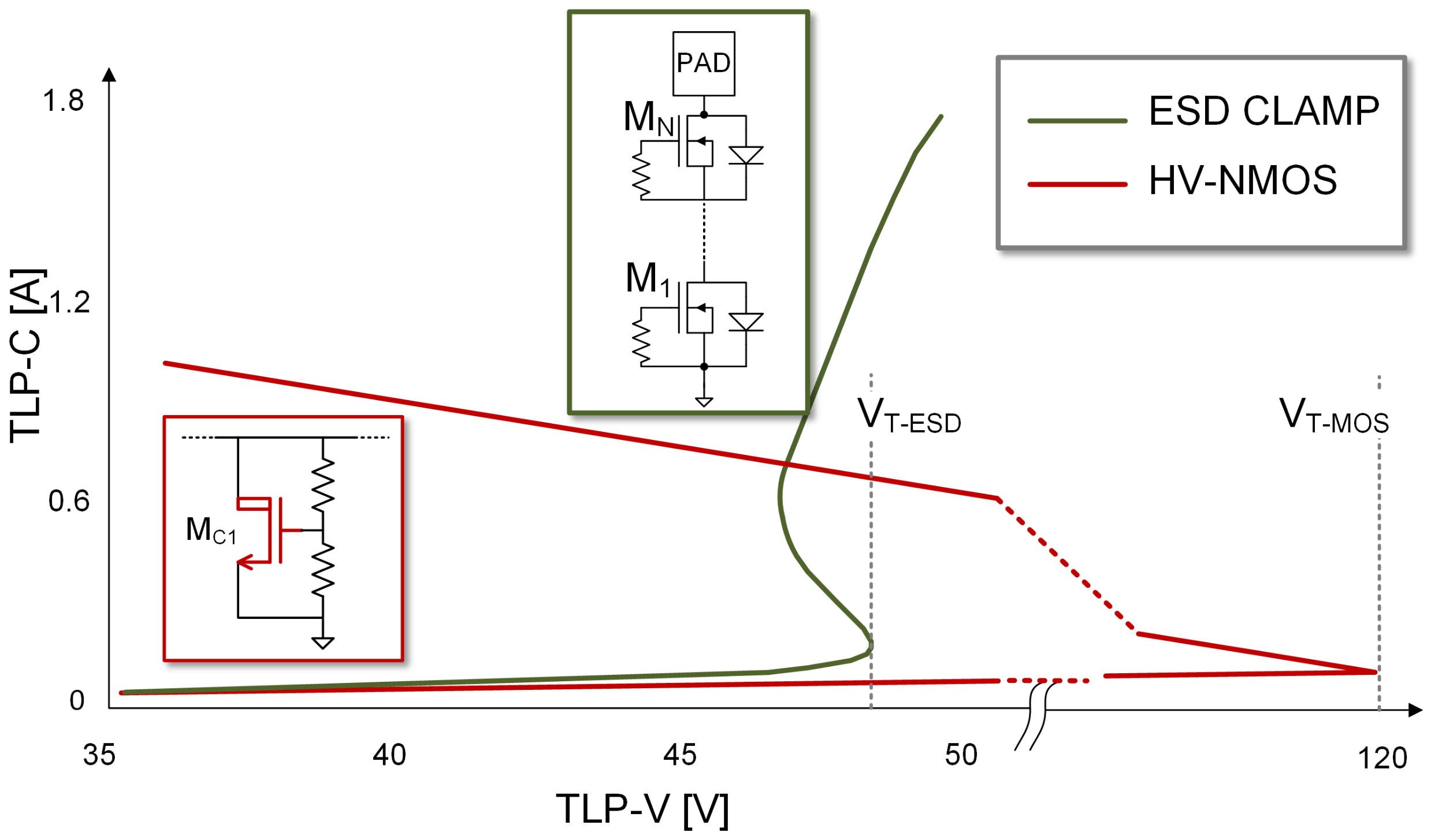
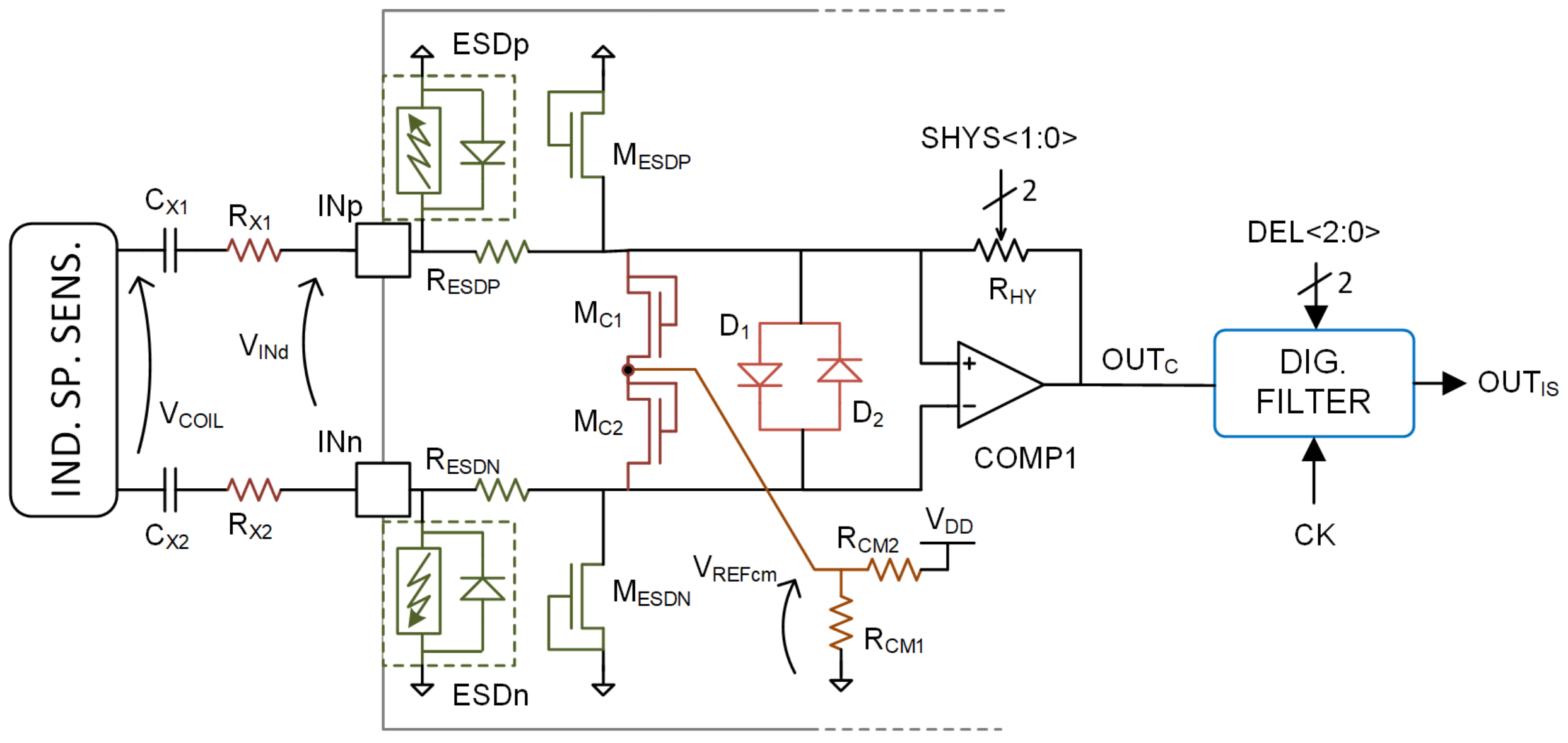
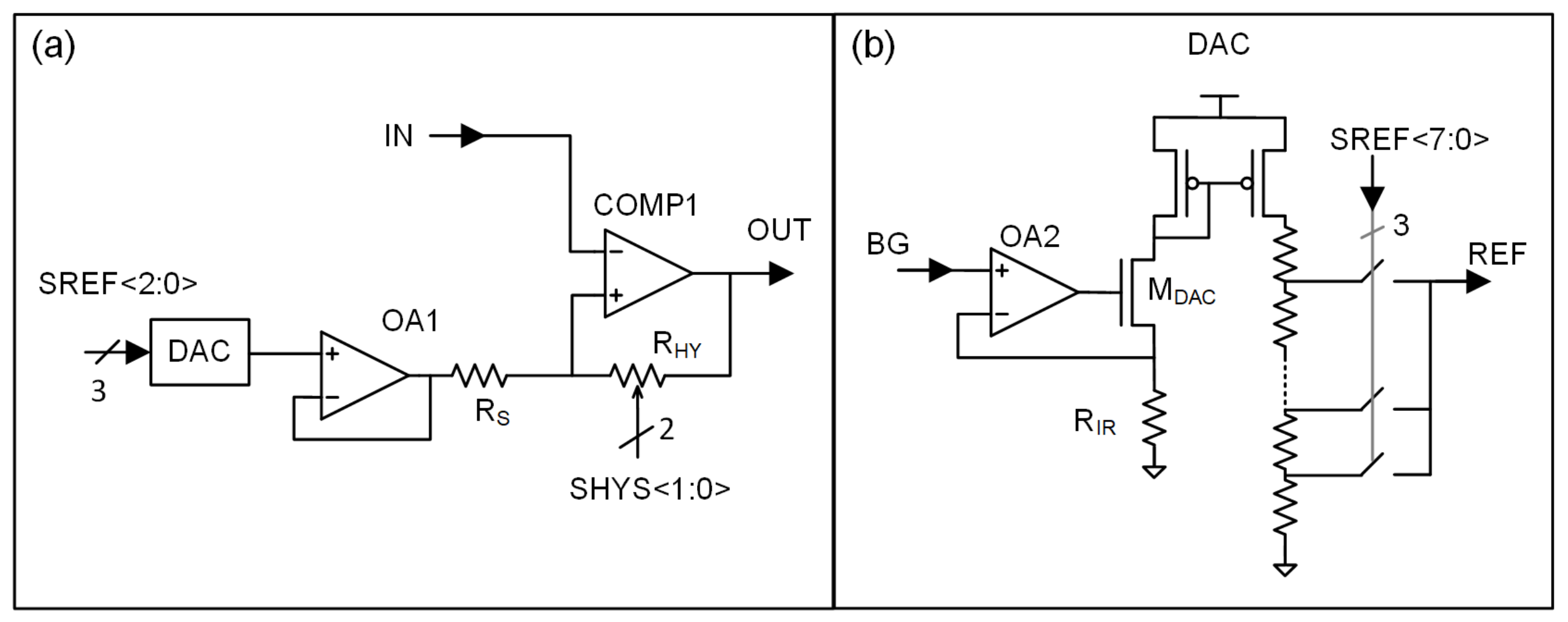
2.2. Integrated Interface Circuit with Multi-Level Voltage Clamping

Sensing the voltage signal at the injector pins or at the low side of the ignition coil raises non-trivial design issues. In the case of the injector low side, the circuit must detect both the rising and falling crossing of a reference voltage usually set at V B A T / 2 . Regarding the igniter coil signal, the reference crossing in the low–high transition is relevant information to assess the ignition time instant. In both cases, the interface circuit should withstand repetitive pulses as high as 100 V and 400 V for the fuel injector and the ignition coil, respectively.
This overvoltage condition is particularly critical for the ESD clamping circuit connected to the pad. An ESD protection circuit can be implemented either with a pair of diodes connecting the input pin to the ground and supply rail [31] or with a bidirectional clamp connecting the pad to the ground rail. The former solution is not suitable for protecting the interface circuits in automotive applications, where over-battery conditions often occur, as in the case of igniter or injector signals. Indeed, the diode connected to the supply rail would be forward-biased in such a case. Furthermore, the input signal may be present also when the device is disconnected from the 5 V regulated supply.
In CMOS technologies, bidirectional clamps to ground are often based on gate-grounded NMOS (GGNMOS) [32,33], gate-coupling NMOS (GCNMOS) [34], or RC-triggered NMOS [35,36]. The voltage at the protected pad is limited either by the breakdown or the snap-back activation of the ESD clamp. The dominant clamping mechanism depends on the time derivative of the input signal, with the snap-back promoted by a fast variation of the input voltage.
The direct sizing of an ESD protection for a breakdown voltage higher than the peak value of the ignition coil or injector signals is not feasible. Indeed, considering a GGNMOS as a clamp device, its drain-to-substrate breakdown voltage must be higher than 400 V. This device is seldom available in high-voltage CMOS technologies with DMOS transistors with a typical breakdown voltage within 100 V [37]. Additionally, a high breakdown voltage could be obtained by stacking several GGNMOS devices [38,39], but with a significant silicon area penalty. Indeed, the width of each transistor correlates with the number of stacked devices to keep the overall series resistance of the discharge suitable for the target ESD protection level.
The circuit in Figure 4a overcomes the above issues at the cost of an off-chip resistor, and it is suitable to interface high-voltage signal sources with 5 V sensing and processing circuits [32]. A primary clamp is introduced in parallel with ESD protection. This clamp is implemented as a shunt regulator based on the DMOS devices M C 1 and the off-chip high-voltage resistor R X . The feedback network with R C 1 and R C 2 is sized to have the voltage at the drain of M C 1 lower than the breakdown voltage of the ESD protections up to a maximum input current I I N m a x . This current limit depends on the aspect ratio of M C 1 , considering that the gate-oxide breakdown constrains its gate-source voltage. It is worth noticing that the proposed interface does not require any MOS devices with high-voltage gate oxide. Indeed, in the circuit prototyping, a 350-nm technology with DMOS devices with 5 V gate oxide as the only high-voltage option was used. The ESD clamp based on a GCNMOS stack was sized for a minimum breakdown voltage of 50 V, and a DMOS transistor with 70 V maximum drain-source voltage was chosen from the available devices. A shunt regulator implemented in CMOS technology with an off-chip resistor was first proposed for automotive applications in [40]. That design includes an operational amplifier in the control loop with additional costs in terms of power consumption and silicon area, with respect to the resistive feedback in this paper. Additionally, the feedback loop of the regulator in [40] shows a small bandwidth. Hence, it is not suitable to process the signals at the low side of the injector and the ignition coil.
The waveform expected at the pad with a typical ignition-coil signal source is shown in Figure 4c. The primary clamp limits the peak value of the pad voltage, whereas the ESD parasitic diode within the GCNMOS clamps the negative peaks due to signal undershoots. The DMOS-based clamp, effectively protecting the pad against repetitive high-voltage pulses, is not designed to be involved in the current discharge path in the case of an ESD event. Therefore, the snap-back voltage of the DMOS transistor must be well above that of the ESD GCNMOS clamp. The plot in Figure 5 shows the measured transmission line pulse (TLP) characteristics [37,41,42] of the ESD clamp and of the 70 V DMOS device. The relatively large range between the trigger voltages V T - M O S and V T - E S D is suitable to allocate the tolerance due to process corner and temperature, affecting both V T - M O S and V T - E S D . In the circuit of Figure 4a, the resistor R S 1 provides additional protection to M C 1 against ESD discharge, while the GGNMOS device M P C 1 is the secondary ESD protection for the M C 1 gate [43].
The signal at the primary clamp cannot be directly provided to the 5 V supply comparator, since it would cause the oxide breakdown of the input MOS devices. Therefore, the signal is scaled down with the resistive attenuator R A 1 R A 2 , considering the value of the clamping voltage at the maximum input current, V C L in Figure 4c, which is affected by the process-and-temperature (PT) variations. A possible strategy is to size the attenuation for the maximum clamp voltage over the P-T range. Nevertheless, with a voltage equal to V B A T at the input pin, the signal level at the comparator input would be significantly lower than the chip supply at the typical PT corner. This effect is highlighted in Figure 4c,d, where V C L S corresponds to V B A T . It should be noticed that the lower V C L S , the lower the noise margin of the comparator detecting the input-signal crossings of V T H = V B A T /2. Thus, the attenuation provided by R A 1 R A 2 is sized to have V C L S = V D D with the typical value of the clamping voltage V C L , leading to a comparator threshold V T H C equal to V D D / 2 . Furthermore, a secondary clamp M P 2 is introduced at the comparator input to limit V C L S at approximately V D D , also in the case of a clamping voltage V C L exceeding the battery voltage, due to PT variations. This secondary clamp is based on a PMOS device with the gate voltage provided through the resistive network R P 1 R P 2 and set to approximately V D D + V T P , with V T P corresponding to the threshold voltage of M P 2 . The final waveform at the comparator input is shown in Figure 4d. It is worth noticing that this combination of two clamping circuits and signal attenuator properly protects both the ESD clamps and the comparator against the repetitive 100 V signal peaks, without affecting the detection of the threshold crossings.
The relevant information of the signal at the high side of the injector in a GDI or a CRDI is the crossing of a threshold placed well above a car-battery voltage to detect the activation of the high-side transistor connected to the high-voltage rail. Therefore, the proposed interface circuit in Figure 4a is not suitable, since the relevant part of that signal, i.e., from t B to t C in Figure 1b, would be clamped slightly above the car-battery voltage. The dedicated interface circuit is shown in Figure 6a, where the resistive attenuators made by the off-chip resistor R X and the on-chip resistors R A 1 and R A 2 , with the control signal A T T tied to the supply voltage, introduces an attenuation factor at the pad, K I N , and at the comparator input, K I N C , equal to:
K I N V H S V I N = R A 1 + R A 2 R X + R A 1 + R A 2
K I N C V H S V I N = R A 2 R X + R A 1 + R A 2
Setting the K I N C factor to 16 allows the scaling down of the input signal in Figure 1b, fitting the maximum signal swing allowed at the comparator input, i.e., the 5 V supply V D D . The tolerance affecting the attenuation factor K I N C due to the PT variations of the integrated resistors R A 1 and R A 2 should be considered. Additionally, the peak value of the voltage signal to be sensed is affected by a significant variation among different injector models and driving circuits. Thus, to prevent the signal at the comparator input exceeding the 5 V supply voltage, a dedicated clamp, based on PMOS M P 2 , is added to the interface circuit of Figure 6a. As for the secondary clamp in Figure 4a, the clamping voltage V C L S is set at the supply voltage by the resistor network R P 1 and R P 2 . Resistor R A 1 is added to inhibit the discharge current path through M P 2 in the case of ESD events. The MOS switch M P 3 allows the disabling of the internal attenuator. In this case, an additional off-chip resistor R X 2 is required to restore the voltage attenuation. This configuration must be used when the K I N C factor is tailored to a specific injector device. Indeed, oversizing K I N C leads to a smaller signal swing at the comparator input, thus forcing the voltage threshold to be lower than V D D /2. By contrast, if K I N C is higher than the optimum value, the signal swing would be strongly limited by the PMOS clamp, and the detection threshold should be increased towards the 5 V supply. In both cases, the noise margin is significantly reduced with respect to the optimum attenuation factor, leading to a detection threshold equal to V D D /2.

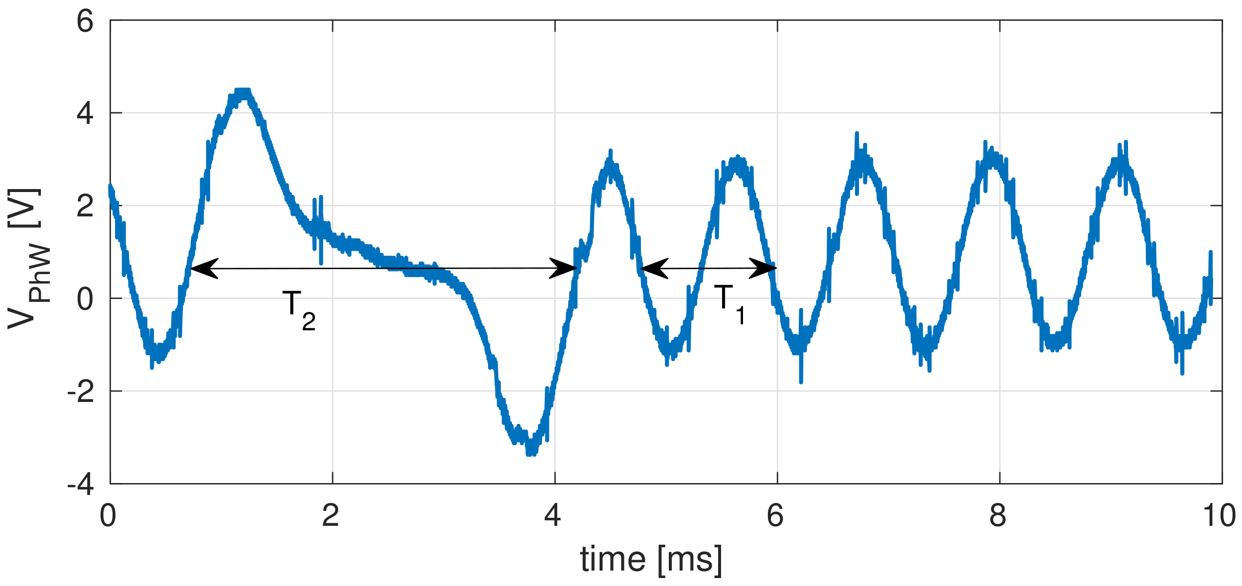
2.3. Inductive Phonic-Wheel Sensor

The angular position and rotation speed of the engine crankshaft is measured by a variable-reluctance sensor installed close to a phonic wheel [44,45]. This element is a toothed wheel connected to the crankshaft with N T H uniformly spaced teeth and two missing teeth [46]. The inductive sensor provides a differential voltage signal, with a frequency proportional to the rotation speed, measured in rotations per minute (RPM). As shown in Figure 7, the period of the output signal increases from T 1 to T 2 when the sensor detects the missing teeth on the wheel. Thus, this abrupt frequency variation allows the obtaining of the absolute angular position of the crankshaft.
The output signal ranges from a few hundred millivolts up to approximately 200 V. The value depends on the actual RPM of the engine: the higher the rotation speed, the larger the output signal. This large range raises a relevant design issue since the interface must withstand an input voltage larger than 100 V, maintaining adequate signal detection capability over three-order magnitude variation of the input signal. Another challenge in the design of the interface circuit comes from the input-signal waveform, very different from an ideal sine wave. Indeed, the shape of the output waveform depends on the design of the teeth. The green trace in the oscilloscope snapshot in Figure 8 corresponds to a signal shaped with a sequence of a positive and a negative pulse followed by a relatively long time interval, with the sensor output voltage close to the reference level, i.e., 0 V. The orange trace in the same figure corresponds to the expected output of the readout circuit detecting the crossings of the reference level to obtain the crankshaft position and its RPM speed.
The proposed interface circuit for the variable-reluctance sensor is shown in Figure 9. The only off-chip components are the AC-coupling capacitors C X 1 and C X 2 and the current-limiting resistors R X 1 and R X 2 . Antiparallel diodes D 1 and D 2 are introduced to limit the differential input voltage of the comparator to either −0.7 V or +0.7 V. The off-chip resistors are sized to have the maximum input current compatible with both the maximum signal amplitude and the current limit set by the metal lines and the involved devices in the current path, i.e., R E S D P , D 1 or D 2 , and R E S D N . The common-mode voltage at the comparator input is set by the voltage divider R C M 1 R C M 2 connected to the center tap of the network with NMOS diodes M C 1 and M C 2 . Such devices act as a common-mode clamp at the comparator input against fast variations of the common-mode voltage level at the sensor output, often exceeding the chip supply voltage. Indeed, with this clamping strategy, the common-mode shift from the reference voltage, generated with R C M 1 and R C M 2 , is limited by the gate-source voltage of M C 1 and M C 2 .
The ESD protection is guaranteed by combining a primary ESD clamp with a secondary one through a 400- Ω resistor, i.e., R E S D P and R E S D N . The former clamp is based on a GCNMOS device [34], while the latter is a GGNMOS, i.e., M E S D P and M E S D N . Using a single device in the primary protection minimizes the silicon area, but limits the breakdown voltage slightly above the 5 V supply. Combining the differential and common-mode clamp guarantees that the voltage at the input pads is always below the 5 V supply, thus avoiding the activation of the primary ESD clamps over the full range of the sensor output signal. Furthermore, the series resistance R E S D P ( R E S D N ) limits the ESD discharge current through the secondary clamp, with adequate protection to the devices at the comparator inputs.

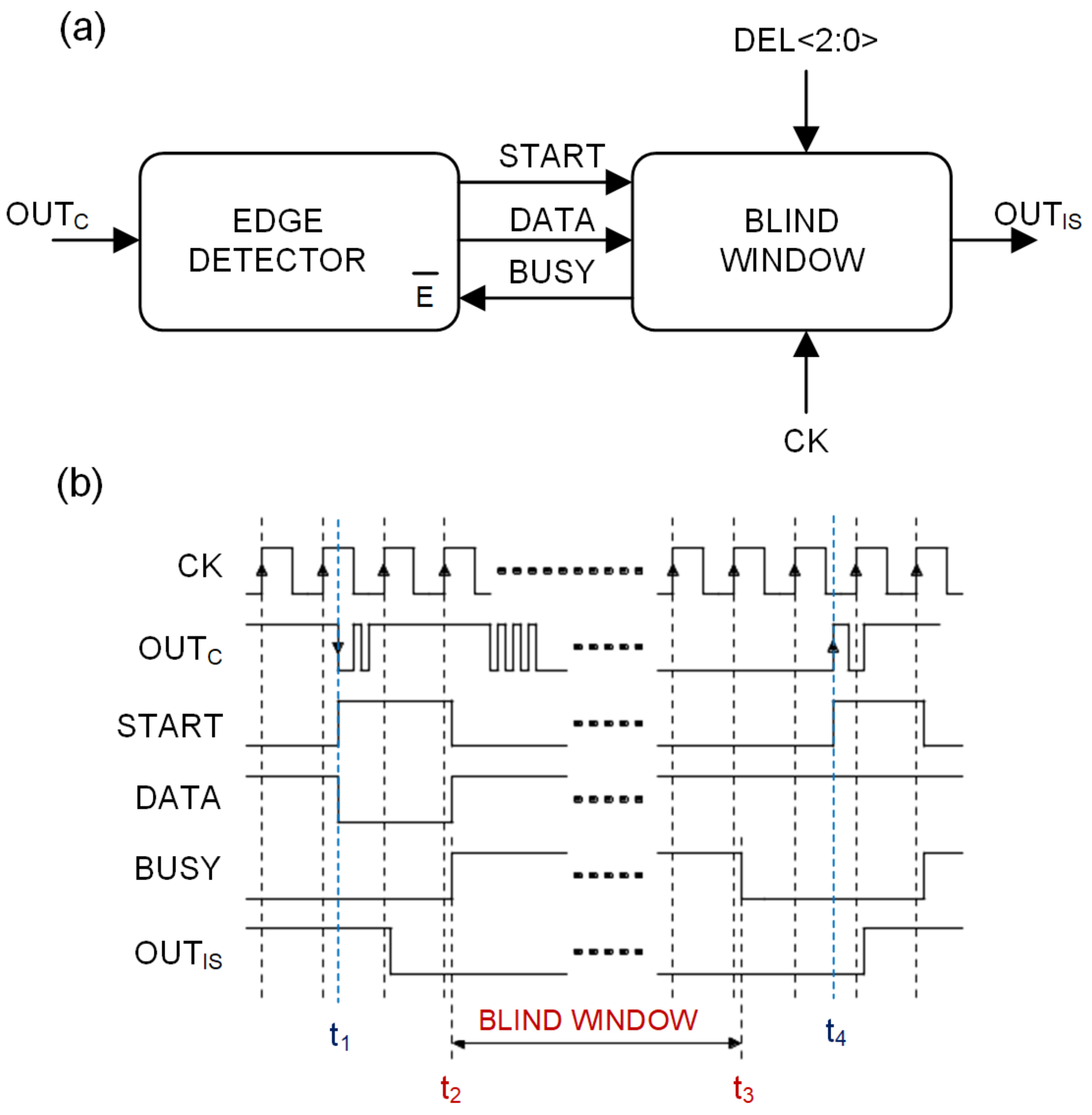
2.4. Conversion and Processing Circuits

In the circuits of Figure 4a and Figure 6a, designed for sensing the signals at the injector pins or at the ignition coil, a comparator is used to detect the crossing of a voltage threshold. Since the signals in the automotive domain are usually affected by ringing and coupled noise, the comparator I/O characteristic must exhibit an adequate hysteresis to prevent the occurrence of multiple output transitions at the crossing point. As shown in Figure 10a, the well-known Schmitt trigger configuration was used. The hysteresis width is set by the ratio R H Y / R S + R H Y , while the threshold is set by the 3-bit digital-to-analog (DAC) converter in Figure 10b. Four values of hysteresis width can be set through the programmable resistor R H Y . The comparator COMP1 is a Miller op-amp without frequency compensation followed by an inverter, while OA1 is a folded-cascode amplifier with rail-to-rail input. The DAC is based on a resistive string biased by a reference current generated with a bandgap voltage reference [47] and resistor R I R . OA2 driving the NMOS M D A C is a folded-cascode amplifier with PMOS input devices. The DAC output voltage is selected from the tap voltages of the resistor string through an array of switches driven with the 1-over-N-coded signal SREF.
The sensing circuit for the phonic-wheel inductive sensor in Figure 9 is based on the same comparator with programmable hysteresis and a fixed reference voltage set to 0 V. Considering the coupled noise affecting the signals from the variable-reluctance sensor and the wide variety of waveforms, determined by the design of the teeth of the phonic wheel, the digital signal at the comparator output is pre-processed on-chip and then sent to the micro-controller in the ECU. Indeed, in the circuit of Figure 9, the signal at the comparator output O U T C enters a digital filter, composed by an asynchronous edge detector and a sampler with programmable blind window, as shown in the schematic of Figure 11a.
The timing diagram of the filter is shown in Figure 11b. After the power-on-reset, both BUSY and START signals are low. The edge detector is enabled to detect the first transition, either rising or falling, occurring at the comparator output, i.e., t 1 in the timing diagram. After the value of DATA is updated according to the transition detected at the input, START goes high, and the edge detector enters in the standby mode, thus skipping all the successive input transitions. Afterwards, at the first rising edge of the system clock CK, i.e., t 2 , DATA is sampled, the filter output O U T I S is updated, and BUSY toggles to the high value. Just after the updates of DATA at the actual value of the comparator output, the new BUSY value disables the edge detector. Therefore, from the rising transition of BUSY, t 2 , the digital filter stops tracking the comparator output, thus skipping any undesired toggling due to noise, ringing, and crosstalk. This blind window ends at t 3 when BUSY returns to low. From this instant on, the edge detector is enabled to detect the next transition at the comparator output at t 4 , when DATA is updated to match the input value after the detected transition. The length of this blind window is programmable with the 3-bit input DEL from 0 s to 192 µs, with a 5-MHz clock reference. It is worth noticing that the programmability of both the comparator hysteresis and blind-window length makes the proposed interface circuit suitable for almost all the phonic-wheel sensors available on the automotive market.

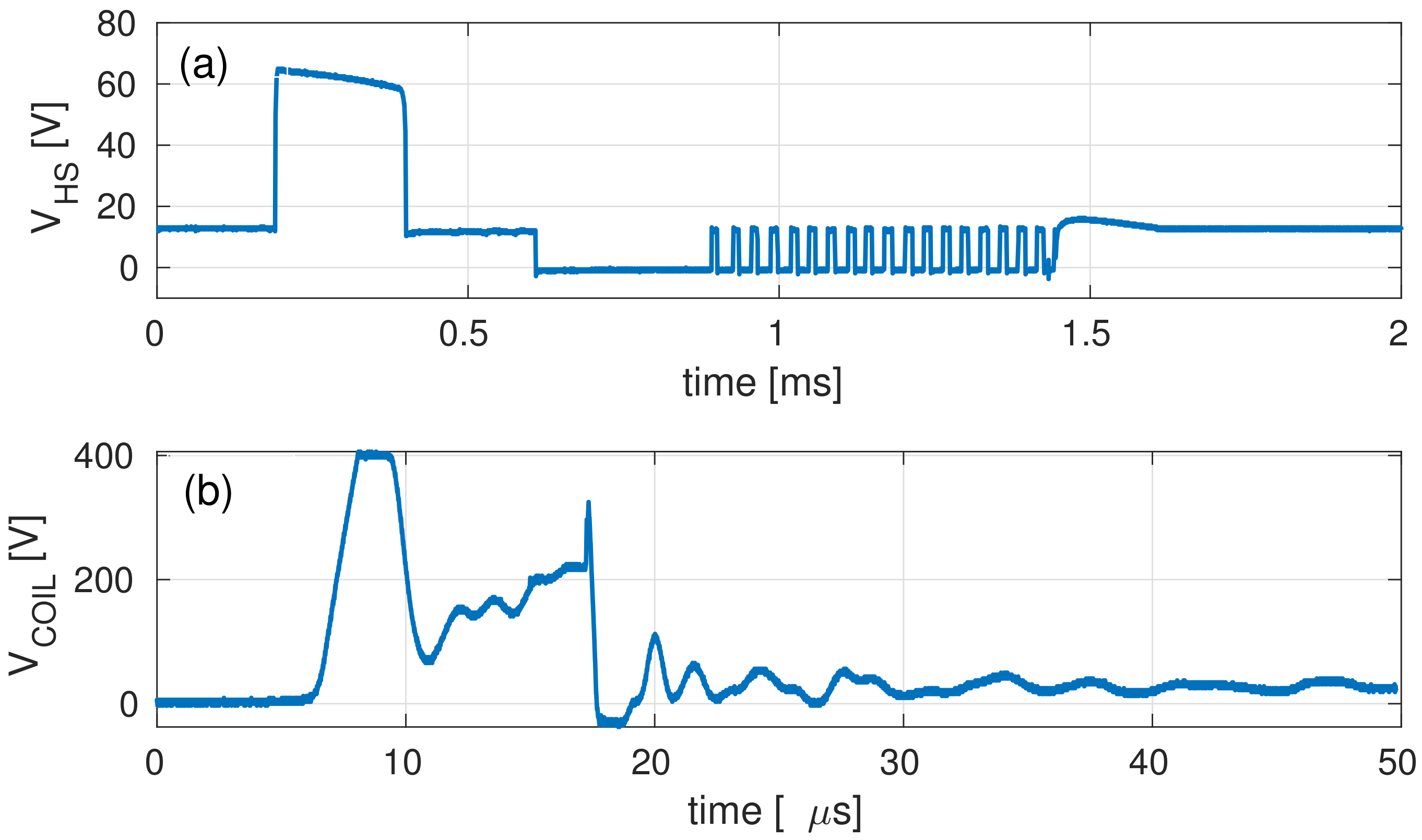
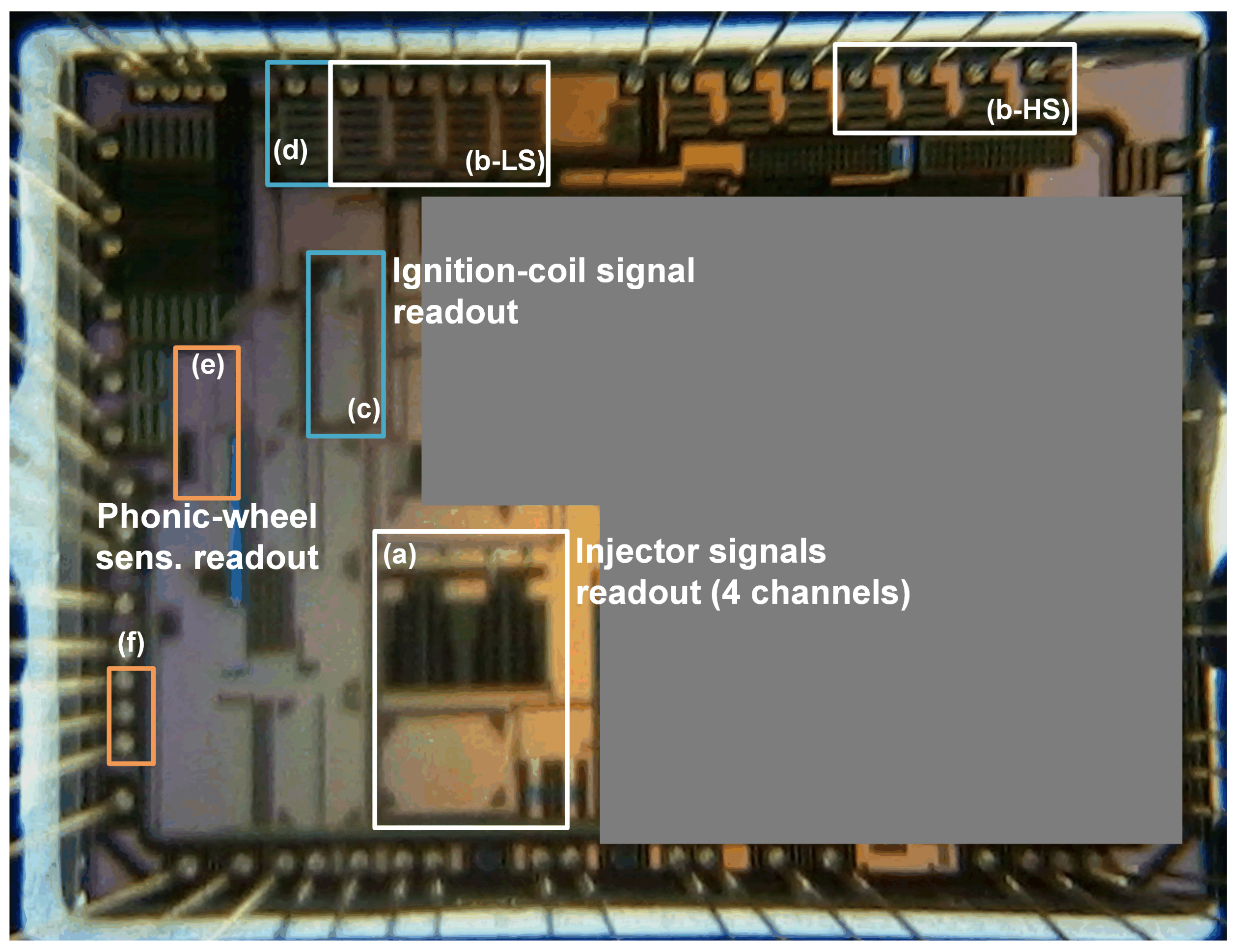
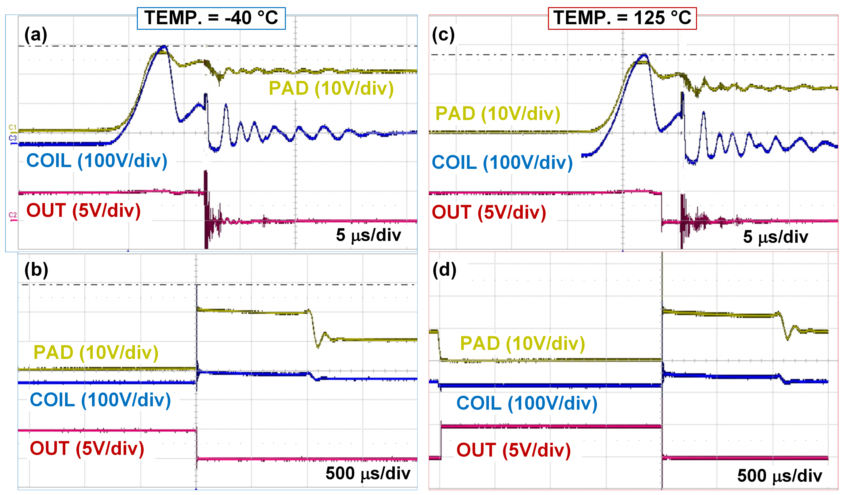
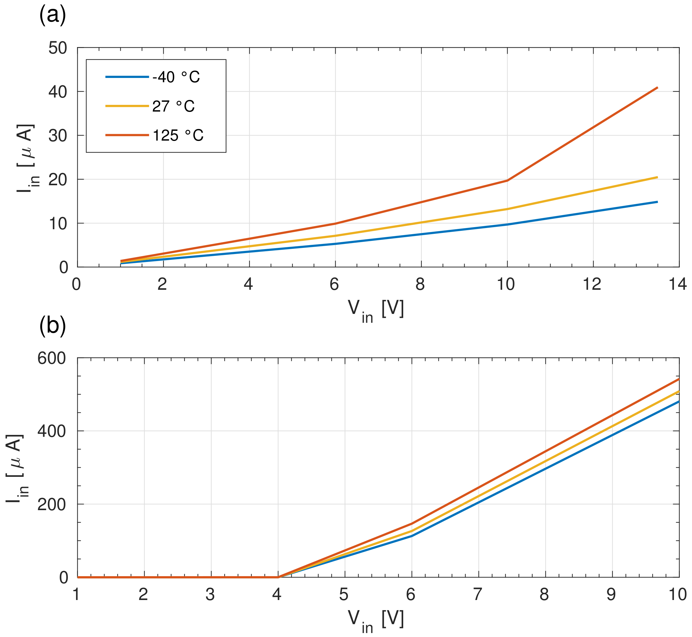
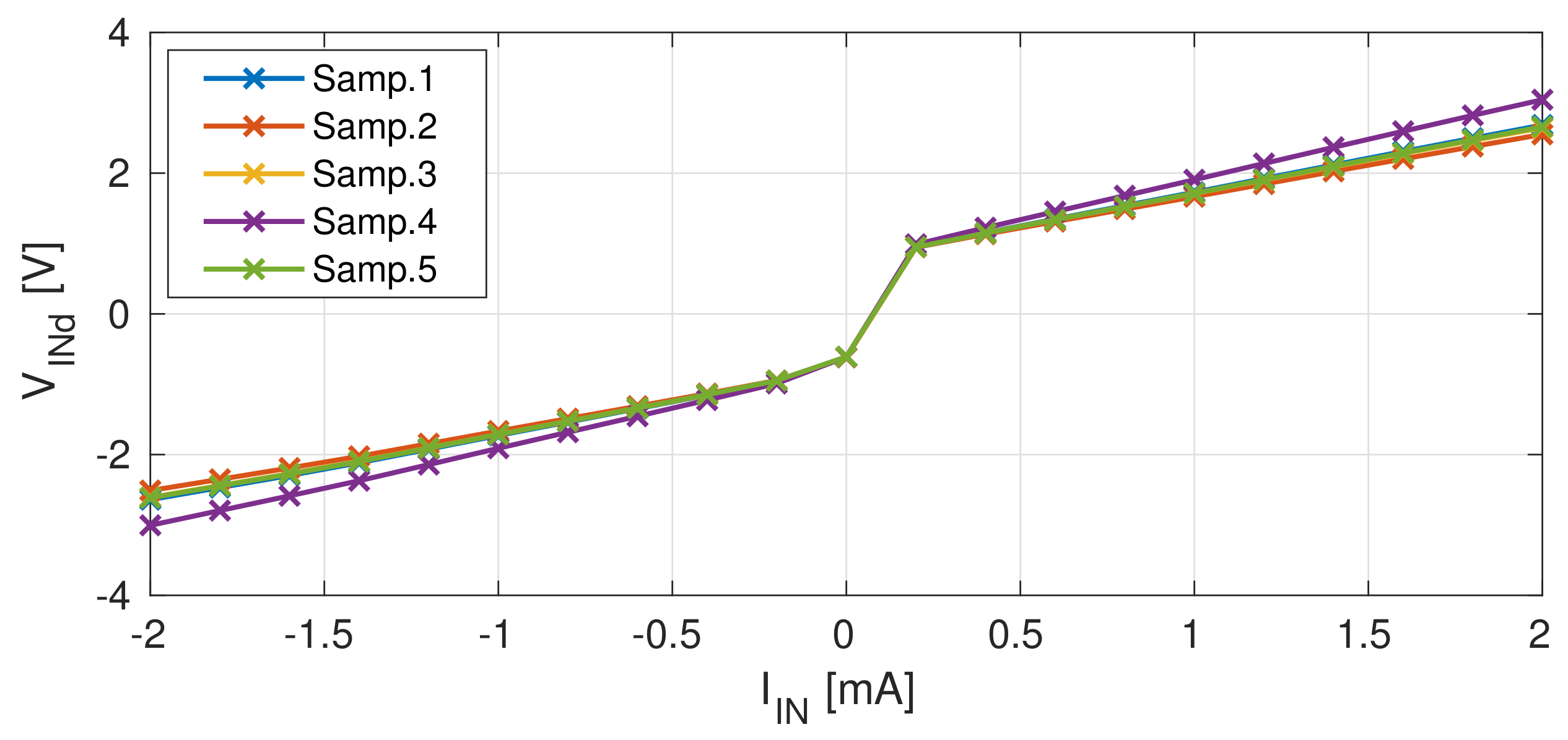
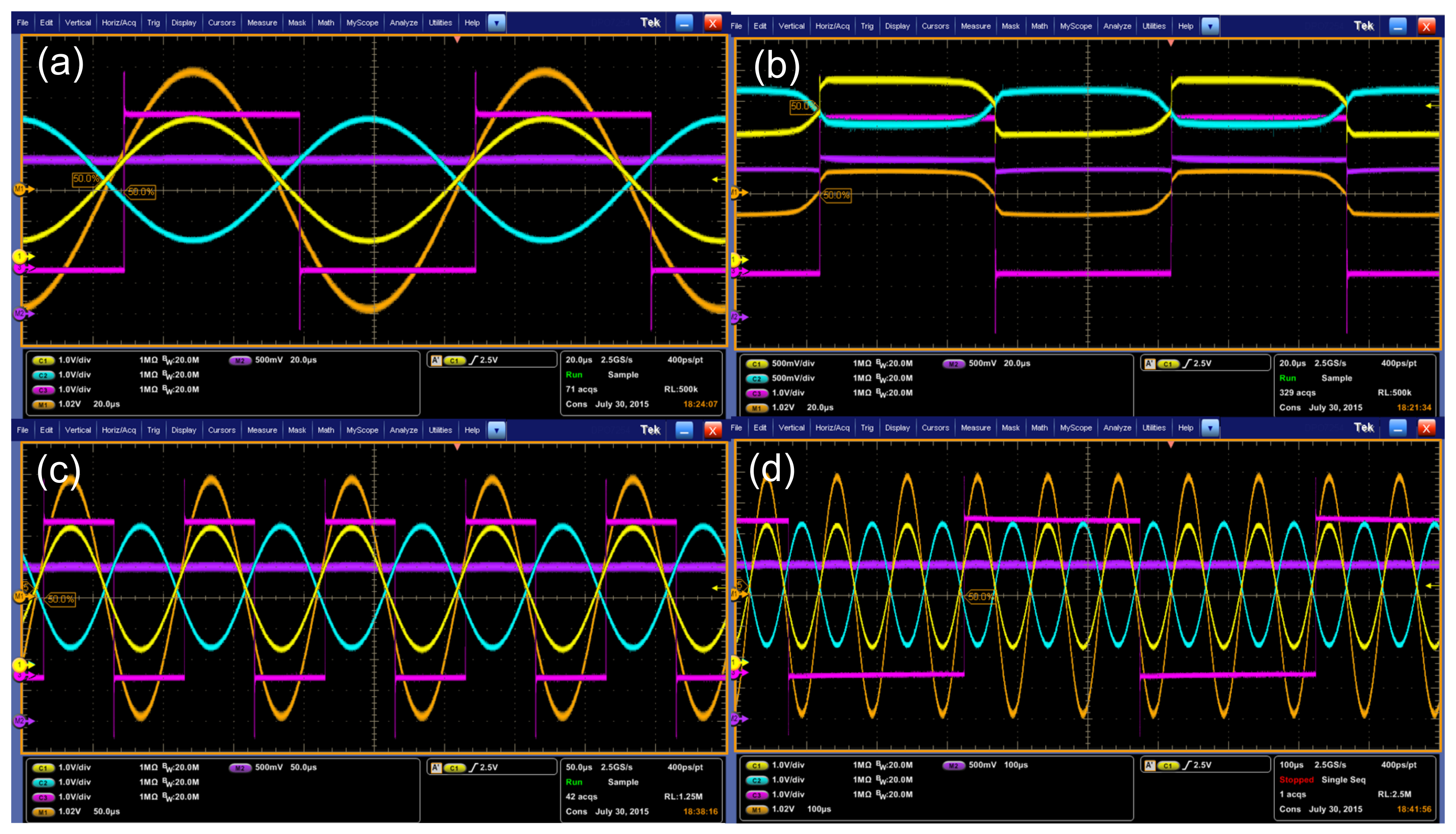
3. Experimental Results

The interface and readout circuits described in Section 2 were implemented in the XFAB 350 nm CMOS technology with 5 V core devices. The only high-voltage option was the DMOS device with 5 V gate oxide and maximum drain voltage that can be set from 20 to 70 V. The very highly resistive polysilicon layer, for megaohm resistors, and a high-density metal–insulator–metal (MIM) capacitor were the analog options used in this design.
The silicon prototype in Figure 12, including other circuits not presented in this paper, is a complete device integrating a large section of a gas-ECUs for the conversion of a car or truck engine from gasoline to gas (LPG, CNG, or hydrogen) or from diesel to a mixture of diesel and gas [5,6,48,49].
All the pins to be connected to the main ECU, or to sensors, actuator terminals (e.g., fuel injectors), and any devices outside the dedicated gas-ECU, exhibit 8 kV HBM ESD protection level.
The white boxes (a) correspond to the circuit for the low- and high-side injector signals (four channels). The ESD protections and the eight pads are in the white boxes (b-LS), i.e., low-side inputs, and (b-HS), i.e., high-side inputs. The larger area of pads and ESD clamps for the low-side inputs is due to the required higher breakdown voltage, i.e., 50 V against 30 V for the high-side inputs. The readout circuits for the ignition-coil signal are in the blue box (c) with the ESD clamp (50 V breakdown) and pad in box (d). Orange boxes (e) and (f) refer to the readout circuit and 5 V pad with ESD clamp for the phonic-wheel inductive sensor.
The plots in Figure 13 show the measured voltage at the input pin of the interface circuit for the ignition-coil or the low-side injector signal. Since the metal input line and the drain contacts of M C 1 in Figure 4a are sized for a maximum current of 2 mA, from the measurement results in Figure 13a, a maximum source voltage V S as high as 400 V is tolerated by the interface circuit without any damage, or a significant shift of the input leakage current. In the case of a negative source signal, the drain-to-substrate diode of the GC-NMOS devices in the ESD clamp, i.e., M N to M 1 in Figure 5, is forward-biased. Considering the large diode area, a current of 100 µA can be tolerated without affecting the ESD devices. Therefore, with a 220-k Ω series resistor, a negative source voltage lower than −10 V can be tolerated by the interface circuits.
The circuit in Figure 4a was tested in a dedicated ECU, interfaced to the low- and high-side pins of the injector, to the ignition coil, and the phonic-wheel sensors of a GDI engine. The oscilloscope snapshots in Figure 14 shows the signal at the ignition coil (blue trace), with a peak value of approximately 350 V, and the signal at the input pin, properly limited below 30 V (yellow trace) by the proposed clamp. The input and output signals were acquired at the minimum and maximum temperatures of the automotive range, i.e., −40 ° and 125 ° . For these measurements, the device with the test-board was placed in a climatic chamber and the input signal was provided by an emulator of automotive signals (located outside the chamber).
The plots in Figure 15a show the measured input current of the same interface circuit vs. the forced input voltage at the minimum, typical, and maximum temperatures. The typical and maximum values of the input current at 10 V input are 14 and 21 µA, respectively. The sensitivity of the input current to the temperature is mainly due to the clamp device M C 1 acting in the circuit as a shunt regulator. In particular, the negative temperature sensitivity of the voltage threshold of the clamp causes the positive temperature coefficient of the input current, at a fixed input voltage. Considering the 220-k Ω series resistor and the measured input current, a voltage of 10 V at the input pin corresponds to a source voltage of 13 V and 14.4 V, at 27 °C and 125 °C, respectively. Therefore, the measured input current with V B A T = 12 V at the source is suitable for the target application and does not affect the functionality of the circuit to be monitored, i.e., ignition-coil and injector drivers.
The measured input current of the interface circuit sensing the voltage at the injector high side is shown in Figure 15b. In the measurement, the on-chip attenuator R A 1 R A 2 was disabled. The high input current at input voltages higher than 5 V is due to the low-voltage clamp M P 2 . However, this clamp is not activated by the high-voltage source signal, thanks to the resistive attenuator, either on- or off-chip. The most relevant specifications of the interface and sensing circuit of Figure 4a and Figure 6a are summarized in Table 1, where the parameter V T H R is the equivalent threshold voltage at the source output, i.e., at the left pin of the off-chip resistor R X .
The circuit interfacing the phonic-wheel inductive sensor was experimentally characterized by sweeping the input current and monitoring the differential input voltage with a source and measurement unit device (SMU). The measurement results are shown in Figure 16. The clamping diodes D 1 and D 2 in Figure 9 are implemented as vertical NPN BJT with the base and collector shorted and the emitter area sized for 2 mA maximum current. It is worth noting that the input voltage is due to the voltage drop across the forward-biased diode, either D 1 or D 2 , and the resistors between the primary and secondary ESD clamps, i.e., R E S D P and R E S D P . The measurement results in Figure 16 show that the maximum 2 mA input current leads to a maximum pad voltage below 5 V over the full temperature range. Therefore, 5 V ESD protections have been used to save silicon area. Moreover, considering the off-chip 100 k Ω resistors R X 1 and R X 2 , the maximum input current corresponds to 400 V at the sensor output, which is a convenient value to make the proposed interface compatible with almost all the phonic-wheel inductive sensors available on the market for automotive applications.
The proposed interface circuit was tested with a differential sine-wave signal emulating the output of an inductive sensor. The oscilloscope screenshots with a blind-window length set to 6.4 µs, 190 µs, and disabled are shown in Figure 17a,c,d. The clamping effect of D 1 and D 2 is clear in the oscilloscope screenshot in Figure 17b, showing the signals at I N p and I N n for the same setup.

4. Conclusions

This paper proposed the design and implementation in 350 nm CMOS technology of interface circuits for the acquisition of high-voltage signals in internal-combustion engines. ESD and the over-battery voltage clamps were co-designed to obtain adequate protection, without affecting the time-crossing detection of automotive signals. In particular, the following signals were considered: the voltage at the low and high side of the fuel injector, the voltage of the ignition coil, and the output of the variable-reluctance sensor for the measurement of the crankshaft rotation speed. The circuit solutions proposed in this paper provide input protection and proper signal detection, minimizing the number of external components for maximum integration. This allows area reduction and improved performance, with respect to the currently adopted solutions in dedicated ECUs for the conversion of the engine to gas combustion.

Author Contributions

Conceptualization, A.B. and M.T.; Data curation, M.T.; Formal analysis, A.B., M.C. and M.T.; Supervision, A.B.; Validation, A.M.; Writing—review and editing, A.B. and M.C. All authors have read and agreed to the published version of the manuscript.

Funding

This research received no external funding.

Conflicts of Interest

The authors declare no conflict of interest.

References

  1. Karthic, S.; Senthil Kumar, M. Experimental investigations on hydrogen biofueled reactivity controlled compression ignition engine using open ECU. Energy 2021, 229, 120787. [Google Scholar] [CrossRef]
  2. Kong, F.; Zhang, L.; Zeng, J.; Zhang, Y. Automatic Measurement and Control System for Vehicle ECU Based on CAN Bus. In Proceedings of the 2007 IEEE International Conference on Automation and Logistics, Jinan, China, 18–21 August 2007; pp. 964–968. [Google Scholar] [CrossRef]
  3. Electronic Engine Control Unit. Available online: https://www.bosch-mobility-solutions.com/en/solutions/control-units/eengine-control-unit/ (accessed on 3 February 2022).
  4. Garrard, M.; Gao, L.; Leiss, K.; Gryska, H. MPC563xM-Based Cost Effective ECU Chipset. NXP. Available online: https://www.nxp.com/docs/en/application-note/AN4454.pdf (accessed on 20 February 2022).
  5. Adiyasa, I.W.; Firmansyah, E.; Cahyadi, A.I.; Kautsar, A. Design of Simple ECU for LPG Fuel Injection on Conventional Generator Set. In Proceedings of the 2018 4th International Conference on Science and Technology (ICST), Yogyakarta, Indonesia, 7–8 August 2018; pp. 1–6. [Google Scholar] [CrossRef]
  6. Navale, S.J.; Kulkarni, R.R.; Thipse, S.S. An experimental study on performance, emission and combustion parameters of hydrogen fueled spark ignition engine with the timed manifold injection system. Int. J. Hydrogen Energy 2017, 42, 8299–8309. [Google Scholar] [CrossRef] [Green Version]
  7. Sopena, C.; Diéguez, P.; Sáinz, D.; Urroz, J.; Guelbenzu, E.; Gandía, L. Conversion of a commercial spark ignition engine to run on hydrogen: Performance comparison using hydrogen and gasoline. Int. J. Hydrogen Energy 2010, 35, 1420–1429. [Google Scholar] [CrossRef]
  8. Rimkus, A.; Stravinskas, S.; Matijošius, J. Comparative Study on the Energetic and Ecologic Parameters of Dual Fuels (Diesel–NG and HVO–Biogas) and Conventional Diesel Fuel in a CI Engine. Appl. Sci. 2020, 10, 359. [Google Scholar] [CrossRef] [Green Version]
  9. Hernandez, N.M.; Villanueva, E.P. Production, purification and utilization of biogas as fuel for internal combustion engine. AIP Conf. Proc. 2018, 1941, 020009. [Google Scholar] [CrossRef]
  10. Korakianitis, T.; Namasivayam, A.; Crookes, R. Natural-gas fueled spark-ignition (SI) and compression-ignition (CI) engine performance and emissions. Prog. Energy Combust. Sci. 2011, 37, 89–112. [Google Scholar] [CrossRef]
  11. Marmiroli, B.; Venditti, M.; Dotelli, G.; Spessa, E. The transport of goods in the urban environment: A comparative life cycle assessment of electric, compressed natural gas and diesel light-duty vehicles. Appl. Energy 2020, 260, 114236. [Google Scholar] [CrossRef]
  12. He, X.; Wallington, T.J.; Anderson, J.E.; Keoleian, G.A.; Shen, W.; De Kleine, R.; Kim, H.C.; Winkler, S. Life-Cycle Greenhouse Gas Emission Benefits of Natural Gas Vehicles. ACS Sustain. Chem. Eng. 2021, 9, 7813–7823. [Google Scholar] [CrossRef]
  13. Wilberforce, T.; El-Hassan, Z.; Khatib, F.; Al Makky, A.; Baroutaji, A.; Carton, J.G.; Olabi, A.G. Developments of electric cars and fuel cell hydrogen electric cars. Int. J. Hydrogen Energy 2017, 42, 25695–25734. [Google Scholar] [CrossRef] [Green Version]
  14. Manoharan, Y.; Hosseini, S.E.; Butler, B.; Alzhahrani, H.; Senior, B.T.F.; Ashuri, T.; Krohn, J. Hydrogen Fuel Cell Vehicles; Current Status and Future Prospect. Appl. Sci. 2019, 9, 2296. [Google Scholar] [CrossRef] [Green Version]
  15. Fayaz, H.; Saidur, R.; Razali, N.; Anuar, F.; Saleman, A.; Islam, M. An overview of hydrogen as a vehicle fuel. Renew. Sustain. Energy Rev. 2012, 16, 5511–5528. [Google Scholar] [CrossRef]
  16. Shadidi, B.; Najafi, G.; Yusaf, T. A Review of Hydrogen as a Fuel in Internal Combustion Engines. Energies 2021, 14, 6209. [Google Scholar] [CrossRef]
  17. Sáinz, D.; Diéguez, P.; Sopena, C.; Urroz, J.; Gandía, L. Conversion of a commercial gasoline vehicle to run bi-fuel (hydrogen-gasoline). Int. J. Hydrogen Energy 2012, 37, 1781–1789. [Google Scholar] [CrossRef]
  18. Thurnheer, T.; Soltic, P.; Dimopoulos Eggenschwiler, P. SI engine fuelled with gasoline, methane and methane/hydrogen blends: Heat release and loss analysis. Int. J. Hydrogen Energy 2009, 34, 2494–2503. [Google Scholar] [CrossRef]
  19. Firmansyah, A.; Aziz, A.R.; Heikal, M.R.; Zainal A., E.Z. Diesel/CNG Mixture Autoignition Control Using Fuel Composition and Injection Gap. Energies 2017, 10, 1639. [Google Scholar] [CrossRef] [Green Version]
  20. Karagöz, Y.; Sadeghi, M.M. Electronic control unit development and emissions evaluation for hydrogen–diesel dual-fuel engines. Adv. Mech. Eng. 2018, 10, 1687814018814076. [Google Scholar] [CrossRef]
  21. Farooqi, Q.R.; Snyder, B.; Anwar, S. Real Time Monitoring of Diesel Engine Injector Waveforms for Accurate Fuel Metering and Control. J. Control Sci. Eng. 2013, 2013, 973141. [Google Scholar] [CrossRef] [Green Version]
  22. Erkuş, B.; Sürmen, A.; İhsan Karamangil, M. A comparative study of carburation and injection fuel supply methods in an LPG-fuelled SI engine. Fuel 2013, 107, 511–517. [Google Scholar] [CrossRef]
  23. Zhang, X.; Palazzolo, A.; Kweon, C.B.; Thomas, E.; Tucker, R.; Kascak, A. Direct Fuel Injector Power Drive System Optimization. SAE Int. J. Engines 2014, 7, 1137–1154. [Google Scholar] [CrossRef]
  24. Tsai, W.C. Optimization of Operating Parameters for Stable and High Operating Performance of a GDI Fuel Injector System. Energies 2020, 13, 2405. [Google Scholar] [CrossRef]
  25. Xiong, J.; Gu, H. An Intelligent Dual-Voltage Driving Method and Circuit For a Common Rail Injector for Heavy-Duty Diesel Engines. IEEE Access 2018, 6, 27681–27689. [Google Scholar] [CrossRef]
  26. Kumar, A.; Kumar, A.; Banerjee, N.; Mohan, N.; Ashok, B. Study of the injector drive circuit for a high pressure GDI injector. In Proceedings of the 2016 International Conference on Recent Advances and Innovations in Engineering (ICRAIE), Jaipur, India, 23–25 December 2016; pp. 1–6. [Google Scholar] [CrossRef]
  27. Visconti, P.; Ventura, V.; Carlucci, A.P.; Strafella, L. Driving electronic board with adjustable piloting signal parameters for characterization of Common Rail diesel injectors with pure biodiesel. In Proceedings of the 2016 IEEE 16th International Conference on Environment and Electrical Engineering (EEEIC), Florence, Italy, 7–10 June 2016; pp. 1–6. [Google Scholar] [CrossRef]
  28. Tang, Q.; Wojslawowicz, J.; Hoenes, H.P. AN-8208 Introduction to Automotive Ignition Systems. Fairchild Semiconductor Corporation. 2014. Available online: https://www.onsemi.com/pub/Collateral/AN-8208CN.pdf (accessed on 20 February 2022).
  29. Kubis, M.; Sebok, M.; Beno, P.; Kucera, M.; Gutten, M. Diagnostics of the ignition system for various fault conditions. In Proceedings of the 2020 International Conference on Diagnostics in Electrical Engineering (Diagnostika), Pilsen, Czech Republic, 1–4 September 2020; pp. 1–4. [Google Scholar] [CrossRef]
  30. Melina, O.M.; STMicroelectronics. Application Note Car Ignition with IGBTs. 1999. Available online: https://www.st.com/resource/en/application_note/an484-car-ignition-with-igbts-stmicroelectronics.pdf (accessed on 20 February 2022).
  31. Ker, M.D. Whole-chip ESD protection design with efficient VDD-to-VSS ESD clamp circuits for submicron CMOS VLSI. IEEE Trans. Electron Devices 1999, 46, 173–183. [Google Scholar] [CrossRef]
  32. Boni, A.; Tonelli, M.; Magnanini, A.; Caselli, M. Fully integrated CMOS overvoltage protection circuit for automotive applications. Electron. Lett. 2015, 51, 1316–1318. [Google Scholar] [CrossRef]
  33. Zeng, J.; Dong, S.; Liou, J.J.; Han, Y.; Zhong, L.; Wang, W. Design and Analysis of an Area-Efficient High Holding Voltage ESD Protection Device. IEEE Trans. Electron Devices 2015, 62, 606–614. [Google Scholar] [CrossRef]
  34. Wang, Y.; Jia, S.; Chen, Z.; Zhang, G.; Ji, L. A design model of gate-coupling NMOS ESD protection circuit. In Proceedings of the 7th International Conference on Solid-State and Integrated Circuits Technology, Beijing, China, 18–21 October 2004; Volume 2, pp. 856–859. [Google Scholar] [CrossRef]
  35. Huang, S.C.; Liao, H.F.; Weng, S.P.; Nidhi, K.; Wang, Y.K.; Chen, Y.J.; Chiou, H.C.; Jou, Y.N.; Lee, J.H.; Liao, C.C. Analyzing Gate-Driven Circuit Parameters for Adding ESD Performances. In Proceedings of the 2019 IEEE International Conference on Consumer Electronics-Taiwan (ICCE-TW), Ilan, Taiwan, 20–22 May 2019; pp. 1–2. [Google Scholar] [CrossRef]
  36. Stockinger, M.; Mertens, R. RC-triggered ESD clamp with low turn-on voltage. In Proceedings of the 2017 IEEE Custom Integrated Circuits Conference (CICC), Austin, TX, USA, 30 April–3 May 2017; pp. 1–4. [Google Scholar] [CrossRef]
  37. Fan, S.K.; Chen, S.L.; Lin, P.L.; Chen, H.W. Layout Strengthening the ESD Performance for High-Voltage N-Channel Lateral Diffused MOSFETs. Electronics 2020, 9, 718. [Google Scholar] [CrossRef]
  38. Worley, E. Stacked ESD Protection Circuit Having Reduced Trigger Voltage. U.S. Patent 2008/0259511 A1, 28 September 2008. [Google Scholar]
  39. Thijs, S.; Scholz, M.; Linten, D.; Griffoni, A.; Russ, C.; Stadler, W.; Lafonteese, D.; Vashchenko, V.; Sawada, M.; Concannon, A.; et al. SCCF—System to component level correlation factor. In Proceedings of the Electrical Overstress/Electrostatic Discharge Symposium Proceedings, Reno, NV, USA, 3–8 October 2010; pp. 1–10. [Google Scholar]
  40. Martins, M.; Dias, J. CMOS Shunt Regulator with Bandgap Reference for Automotive Environment. IEE Proc. Circuits Devices Syst. 1994, 141, 157–161. [Google Scholar] [CrossRef]
  41. Smedes, T.; Velghe, R.; Ruth, R.; Huitsing, A. The application of Transmission Line Pulse testing for the ESD analysis of integrated circuits. In Proceedings of the 2001 Electrical Overstress/Electrostatic Discharge Symposium, Portland, OR, USA, 11–13 September 2001; pp. 421–429. [Google Scholar]
  42. Mergens, M.; Wilkening, W.; Mettler, S.; Wolf, H.; Stricker, A.; Fichtner, W. Analysis of lateral DMOS power devices under ESD stress conditions. IEEE Trans. Electron Devices 2000, 47, 2128–2137. [Google Scholar] [CrossRef]
  43. Vashchenko, V.; Scholz, M. System Level ESD Protection; Springer: Cham, Switzerland, 2014. [Google Scholar] [CrossRef]
  44. Coppo, F.; Pepe, G.; Roveri, N.; Carcaterra, A. A Multisensing Setup for the Intelligent Tire Monitoring. Sensors 2017, 17, 576. [Google Scholar] [CrossRef]
  45. De Oliveira, A.; Moreira dos Santos, E.C.; Botelho, G.C.; Valente, O.S.; Sodré, J.R. Hydrogen electronic injection system for a diesel power generator. Int. J. Hydrogen Energy 2013, 38, 7986–7993. [Google Scholar] [CrossRef]
  46. Laganá, A.A.; Lima, L.L.; Justo, J.F.; Arruda, B.A.; Santos, M.M. Identification of combustion and detonation in spark ignition engines using ion current signal. Fuel 2018, 227, 469–477. [Google Scholar] [CrossRef]
  47. Caselli, M.; van Liempd, C.; Boni, A.; Stanzione, S. A low-power native NMOS-based bandgap reference operating from −55 °C to 125 °C with Li-Ion battery compatibility. Int. J. Circuit Theory Appl. 2021, 49, 1327–1346. [Google Scholar] [CrossRef]
  48. Shanmugam, R.M.; Kankariya, N.M.; Honvault, J.; Srinivasan, L.; Viswanatha, H.C.; Nicolas, P.; Saravanan, N.; Christian, D. Performance and Emission Characterization of 1.2 L MPI Engine with Multiple Fuels (E10, LPG and CNG). SAE Int. J. Fuels Lubr. 2010, 3, 334–352. [Google Scholar] [CrossRef]
  49. Stepanenko, D.; Kneba, Z. ECU calibration for gaseous dual fuel supply system in compression ignition engines. Combust. Engines 2020, 182, 33–37. [Google Scholar] [CrossRef]
Figure 1. (a): Dual-voltage driver for fuel-injection device in GDI and common-rail engines. (b): Voltage waveform at the high-side terminal. (c): voltage waveform at the low-side terminal. (d): command waveforms of low and high-side switches (high-level corresponds to the closed-state).
Electronics 11 00971 g001
Figure 2. (a): Measured voltage waveform at the high-side of a GDI-engine injector. (b): Measured voltage waveform at the input of the ignition coil.
Electronics 11 00971 g002
Figure 3. (a): IGBT-based driving circuit for ignition coil. (b): voltage waveform at the low-side terminal of the coil.
Electronics 11 00971 g003
Figure 4. (a): Sensing circuit for automotive signals with concurred ESD, over and under voltage protection [32]. (b): Signal at node S. (c): Corresponding signal at the input pad. (d): Signal at the comparator input.
Electronics 11 00971 g004
Figure 5. TLP characteristics of the ESD protection (green curve) and of the primary-clamp DNMOS M C 1 (red curve) in the interface circuit of Figure 4a.
Electronics 11 00971 g005
Figure 6. (a): Interface and readout circuit for the signal at the injector high-side pin (GDI case). (b): Input signal. (c): Signal at the comparator input without the PMOS clamp. (d): Signal at the comparator input with the PMOS clamp.
Electronics 11 00971 g006
Figure 7. Measured output signal of a crankshaft inductive sensor with phonic wheel.
Electronics 11 00971 g007
Figure 8. Output signal of a phonic-wheel inductive sensor with asymmetric rise and fall times.
Electronics 11 00971 g008
Figure 9. Interface and readout circuit for phonic-wheel inductive sensors.
Electronics 11 00971 g009
Figure 10. (a): Comparator with programmable hysteresis and threshold voltage. (b): Schematic diagram of the DAC used to generate the reference voltage for the comparator.
Electronics 11 00971 g010
Figure 11. (a): Black-box schematic of the digital filter for signals from phonic-wheel sensors. (b): Timing diagram.
Electronics 11 00971 g011
Figure 12. Chip photograph. White boxes: four-channel interface and readout circuit for high and low-side injector signals (a) with ESD protections and (b) pads (b-LS and b-HS). Blue boxes: interface and readout for ignition-coil signal (c) with ESD protection and pad (d). Orange boxes: interface and readout for phonic-wheel inductive sensor (e) with ESD protections and pads (f).
Electronics 11 00971 g012
Figure 13. Voltage at the input of the interface circuit with multi-level voltage clamps in Figure 4 vs. input current, at −40 °C, 27 °C, and 125 °C chip temperature. (a) Positive input current sweep; (b) Negative input current sweep.
Electronics 11 00971 g013
Figure 14. Oscilloscope snapshots of the voltage signals at the igniter coil, chip input, and readout circuit output. (a,b) measurements carried out at −40 °C. (c,d) measurements at 125 °C.
Electronics 11 00971 g014
Figure 15. Measured input currents of the circuits for injector signals vs. forced input voltage, at −40 ° , 27 ° , and 125 ° chip temperatures. (a) Input current of the interface circuit for the low-side signal in Figure 4. (b) Input current of the circuit in Figure 6 for the acquisition of the low-side signal.
Electronics 11 00971 g015
Figure 16. Measured differential input voltage V I N d of the interface circuit for inductive speed sensors in Figure 9, with forced input current I I N .
Electronics 11 00971 g016
Figure 17. Readout circuit for inductive speed sensors: measured voltage waveforms. (a) Blind window disabled. Yellow and cyan traces: positive and negative input signals at I N S p and I N S n in Figure 9; orange and violet: differential and common-mode input signals; magenta: output signal of the readout circuit (i.e., at O U T I S S pin). (b) Yellow and cyan traces correspond here to the signals at the inputs I N p and I N n . (c,d) Blind window set to 6.4 µs and to 190 µs, with signals and colors of (a).
Electronics 11 00971 g017
Table 1. Specifications of interface circuits.
MinTyp.MaxUnit
Ignition-Coil or Low-side Injector
R X 220 k Ω
V I N −10 400V
V T H R 1.5 8V
I D D 170 µA
Area with pad 0.27 mm 2
High-side Injector
R X 220 k Ω
R X 2 33 k Ω
V I N −10 180V
V T H R 6 32V
I D D 170 µA
Area with pad 0.08 mm 2
Supply Voltage4.555.5V
Temperature−40 125°C
Publisher’s Note: MDPI stays neutral with regard to jurisdictional claims in published maps and institutional affiliations.

