1. Introduction
The Bandgap Voltage Reference (BGR) is a circuit widely used in most systems on chips producing a reference voltage, theoretically independent of the PVT variations. Older BGR topologies generate a constant voltage reference
Vref equal to 1.25 V, by the sum of the diode bandgap voltage and the thermal voltage multiplied by a factor. In more recent topologies, there has been an increasing interest in BiCMOS or CMOS circuits where the supply voltage tends to be under 1 V and the reference voltage must be below 1 V. So far, very little attention has been given to the generation of an accurate Ready-Indication (RI) signal, indicating that
Vref has reached and is locked in the nominal value. The RI signal is important in a system because it can be used to set the corresponding analog circuits in operating mode. In many recent low power applications, several systems are periodically switched on and off to save power and to increase battery life. In such systems, most circuits must remain off, while BGR is not in ready mode. If the circuits are enabled earlier or later than required, the overall system dissipates power, without being operatable. Currently, more often, a required RI signal or a reset (RST) signal can be generated by a Power-on-Reset (PoR) circuit, which, however, is not accurate and does not indicate whether a reference voltage is also settled and ready for use. Power-on-Reset is a circuit that provides a reset signal when the power supply is initiated and remains in a required voltage range [
1,
2]. Τhe reset signal of a PoR circuit indicates whether the supply voltage is at a normal level so that the analog or mixed circuits are allowed to be enabled but not ensure that a reference voltage can be used. Most PoR systems are simple RC circuits [
1], which, however, are not reliable due to large variations under several processes, voltage, and temperature conditions (PVT).
The PoR circuit and BGR ready indication are critical in analog and mixed signal circuits, only a few reliable solutions are found in the literature. In [
1] a PoR circuit is presented, based on the supply voltage
VDD detection. The supply voltage used in that circuit is greater than 1.8 V, but the threshold trigger voltage is highly sensitive to PVT variations. In [
2] a more accurate, PoR system is proposed which is based on a bipolar transistor pair, similar to that of a BGR. Due to the bipolar transistors, the supply voltage that is used is relatively high greater than 3 V. In [
3] a hybrid bandgap reference is introduced which provides a voltage reference together with a PoR signal. The circuit has the advantage of high simplicity, but due to this, the reference voltage is sensitive over process and voltage variations and the PoR signal is not accurate. In [
4] a BGR ready circuit is proposed for RFID application. The topology is based on two comparators to provide two logic signals about the status of the internal voltages of the specific BGR. However, details about the performance of this circuit under PVT variations are not given. A very simple BGR ready signal is produced in [
5], but this is not accurate as it is based on the startup circuit of the BGR. In [
6] a dedicated BGR for PoR circuit is introduced from 1.3 to 3 V supply voltage.
The drawback of the simple PoR circuits [
1,
2] is that they provide a reset signal only when
VDD crosses the predefined thresholds, though the hybrid BGR-PoR circuits [
3,
4,
5,
6] provide a ready signal with a reference voltage. However, the suggested methods show a high sensitivity over PVT corners and usually dedicated solutions for specific applications are developed in each case. The major problem with producing an accurate RI is that other reliable voltage references that could be used for comparison are not available in the system.
In this paper, a generic method for producing accurate RI signals of the BGRs is proposed. The RI signal indicates that the BGR is settled and produces an accurate Vref which can be used by other circuits. The introduced method is based on the comparison of the voltage reference Vref with some other internal voltages produced by the proposed circuitry. Therefore, only a few additional comparators need to be employed with the BGR. The comparators required in this application can be implemented with simple operational amplifiers and the additional occupation in the layout area is small compared with the BGR core. Additionally, the circuitry generating RI signal does not affect the Vref itself and no noise or other interference is charging it. All comparisons with Vref are isolated through simple operational amplifiers without any feedback from RI to Vref.
The advantages of the introduced method are, first its high accuracy of RI signal, second, it can be employed with already known BGRs from the literature, and third, it can be used to improve even more the accuracy in other already proposed PoR circuits [
3]. Another benefit is that with its flexibility it can be combined with already published in the literature BGR topologies and constitute a substantial solution to provide an accurate RI signal without decreasing the performance of an already efficient BGR. Additionally, using the RI signal for setting in off or in standby mode for other circuits, saves power consumption from the overall system. The cost paid for the extra circuit is the additional area and current consumption, but as already explained both are compensated by the corresponding advantages, the fact that the area is too small, and the overall current consumption of the system can be reduced.
The rest of the paper is organized as follows: In
Section 2, the BGR operation during powerup or down and design approach of BGR RI is discussed. In
Section 3, circuit designs and simulation results are presented for several BGR topologies. The conclusions are given in
Section 4.
2. The Design Approach of BGR RI
During the power-up procedure, the BGR is one of the first circuits starting to operate and must be ready in a short time to provide the reference voltage in the rest circuits of a system, among them in the PoR circuit. During power-up or down the supply voltage
VDD takes a ramp-up or down form, approximately, as shown in
Figure 1. During these time slots, BGR provides an uncertain reference voltage
Vref, especially when the supply voltage
VDD is not yet in the nominal range. In that case,
Vref should be ignored from the rest of the system and a RI signal should decline the start-up of the rest circuits. Usually, a start-up circuit is used in the BGR circuit to ensure that it will start operating normally and will not be latched in off state. In some cases, the start-up circuit could be used as a BGR ready indicator, but this is not enough for an accurate RI signal. The reason is that, for a considerable timeframe, the start-up circuit remains active, while the BGR core internal nodes have already been self-biased, resulting in an uncertain value of
Vref, as shown in
Figure 1. Based on this procedure, a high risk of detecting a possible fault BGR operation mode exists. Under these conditions,
Vref is insufficient to be used as a standalone signal to certify that BGR operates in a normal state and that
VDD has reached its nominal value. Then an appropriate comparison between
Vref,
VDD, and some internal voltages must be performed in order to produce an accurate RI signal.
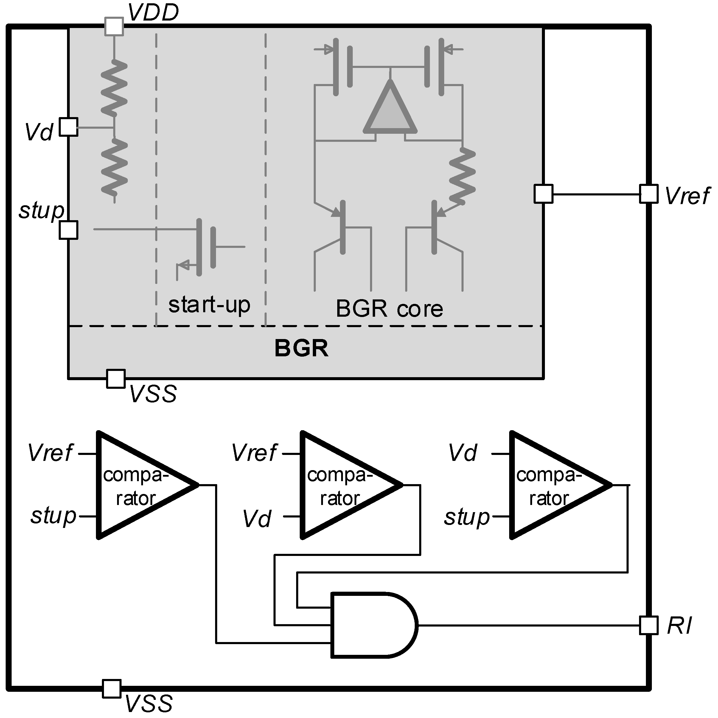
The concept of the required comparisons is depicted in the simplified block diagram of
Figure 2. The internal voltages must be selected carefully, and they must be related to
Vref and
VDD through a known correlation. In
Figure 2,
Vref is the generated reference voltage,
Vd is a proportional voltage to
VDD, and
stup is a voltage generated by the start-up circuit. For most cases, two to three voltage comparisons, between these voltages, are required. The number of comparisons depends on the supply voltage, while the lower voltage headroom makes the procedure harder. It is important that neither voltage nor current can be considered as known or constant during the power-up or power-down procedure, and the comparator’s bias depends on the specific state.
Towards these conditions, the following comparisons must be performed,
- ∘
Comparison between Vref and Vd (proportional to VDD)
- ∘
Comparison between Vref and stup (start-up status)
- ∘
Comparison between stup and Vd (this step is usually needed in low voltage circuits)
However, it must be noted that depending on the particular BGR topology, a similar signal could be utilized instead of one of these described in the steps above. In the following presented topologies, these steps are applied to produce an RI signal.
3. Circuit Design and Simulation Results
The abovementioned observations and obstacles are taken under consideration and applied in three separate topologies, so as the general proposed method to be proved. The first RI circuit has been employed in a BGR topology [
7] shown in
Figure 3. This circuit has been designed and simulated with a 22 nm Fully Depleted Silicon On Insulator (FDSOI) technology node and 1.8 V supply voltage and is presented in
Section 3.1, as BGR#1 (22 nm, 1.8 V). The same topology of [
7] has been also designed and tested in a 65 nm CMOS technology node with 1 V supply voltage and is presented in
Section 3.2, as BGR#1 (65 nm, 1 V). Moreover, other BGR topologies [
3,
8], with different operating conditions have been investigated in order to verify the proposed methodology for the RI. A two operational amplifier based BGR [
8] has been designed in CMOS 65 nm technology node and 1 V supply voltage and is presented in
Section 3.3, as BGR#2 (65 nm, 1 V). Finally, a hybrid PoR-BGR circuit [
3] has been designed in CMOS 65 nm and 0.55 V supply voltage and is presented in
Section 3.4, as BGR#3 (65 nm, 0.55 V).
The proposed BGR circuits have been tested under several power-on and power-off conditions, where the supply voltage VDD is sequentially on and off, through a ramp function with different rise, fall, and settling times at different final voltage levels. The selected temperature ranges, used for the corner simulation results in each design, are extended close to the corners, offered by the corresponding technology for model operation and layout limitations.
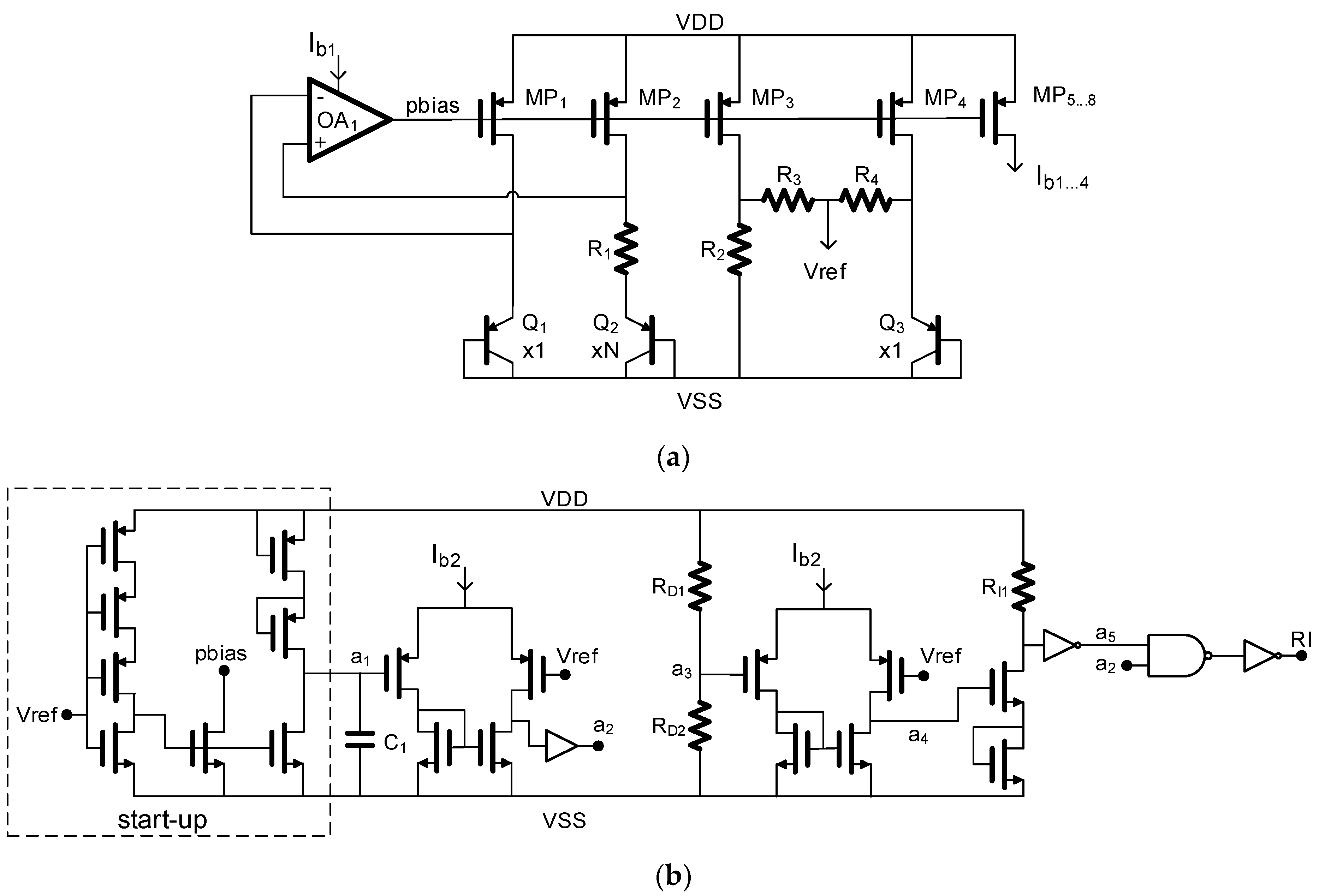
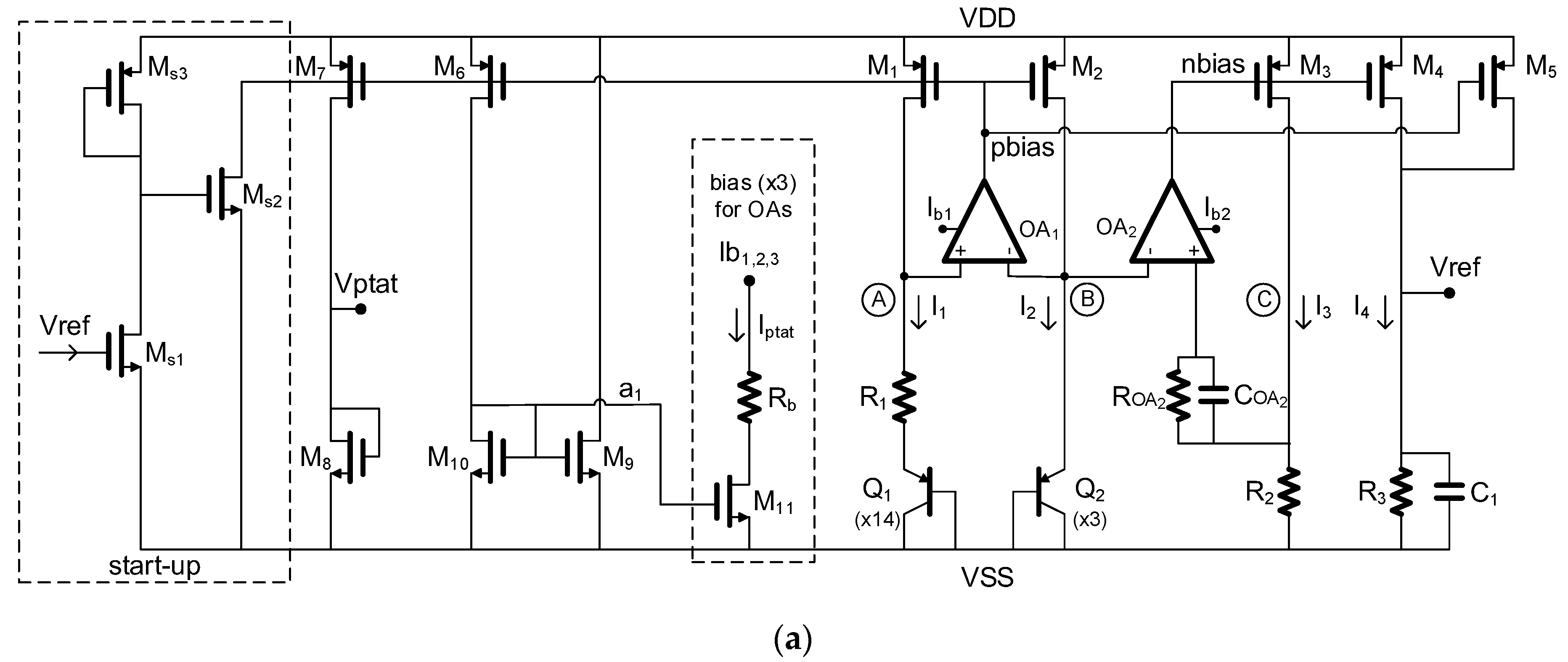
3.1. RI Circuit for BGR#1 in 22 nm, 1.8 V Supply Voltage
For the first BGR [
7] core with the proposed BGR RI circuit, a combination of internal signals is used, being compared with
Vref and resulting in the RI signal, as shown in
Figure 3. The main comparison is realized between
Vref and the
a1 signal generated by the start-up circuit. This comparison ensures that the main bias of the BGR core has already started, and the state of the start-up circuit is off. This comparison, however, is not sufficient because,
Vref could be in a lower level than
a1 but not yet in its nominal value, as the start-up is not in a clear on or off state. A possibly lower than the nominal
VDD could make the BGR start, the start-up circuit be in an off state, but
Vref to be in an unsettled value. Therefore, an additional comparison ensuring that
VDD is within the acceptable range must be performed. The indicative graph of
Figure 1 depicts the unsettled regions where the RI must properly indicate that BGR does not operate in its normal state. A comparison is required between
Vref and
VDD, as well as between
Vref and
a1 generated by the start-up circuit.
The BGR#1 of
Figure 3 has been designed, initially, in a 22 nm FDSOI technology node. Post-layout simulations have been performed to validate the BGR and RI operation. The BGR is tested under several power-up and power-down conditions, where the supply voltage
VDD is sequentially on and off, through a ramp function with different rise and fall times and settling at different final levels. The ramp function has been employed to simulate the way a supply voltage is applied on the circuits in a chip.
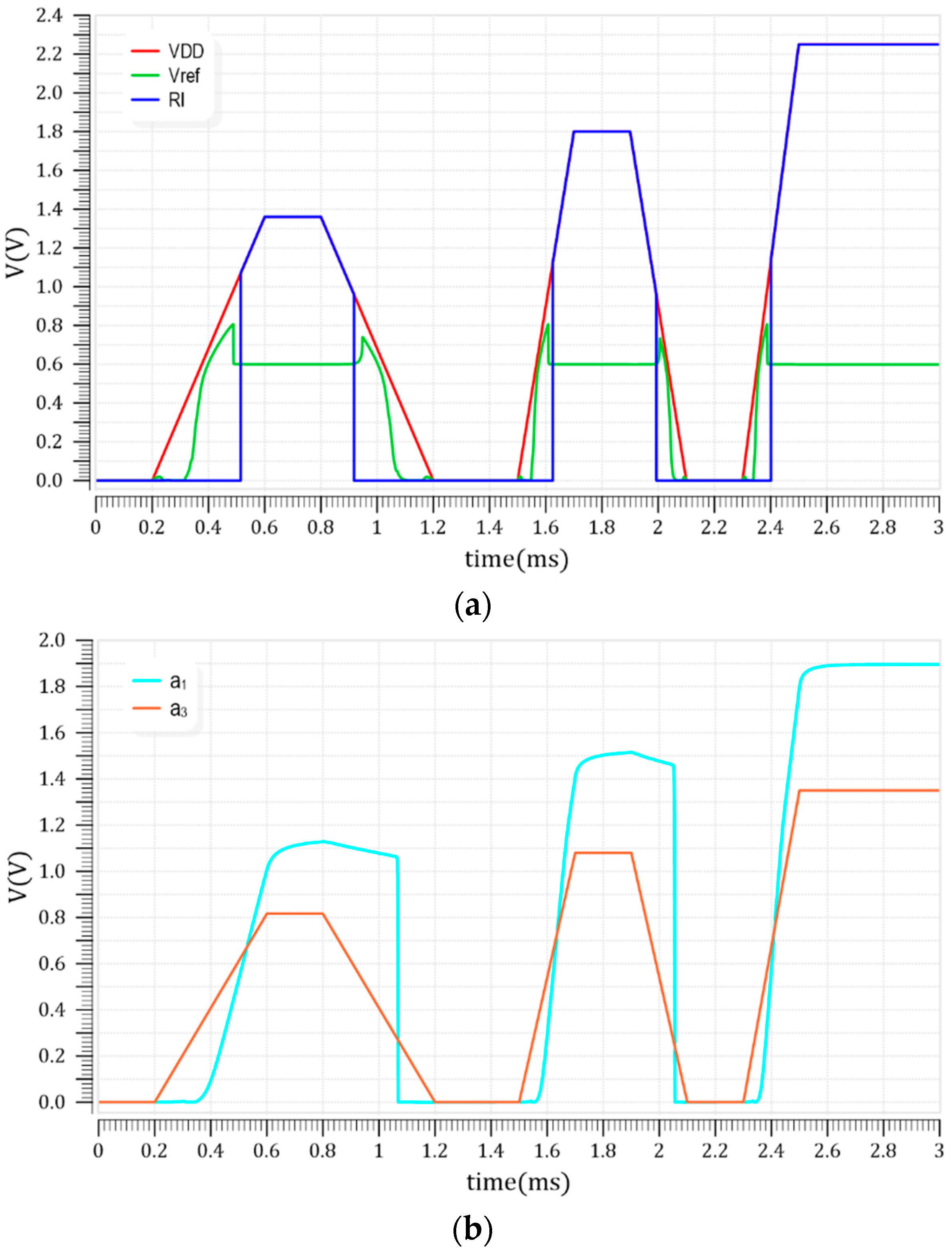
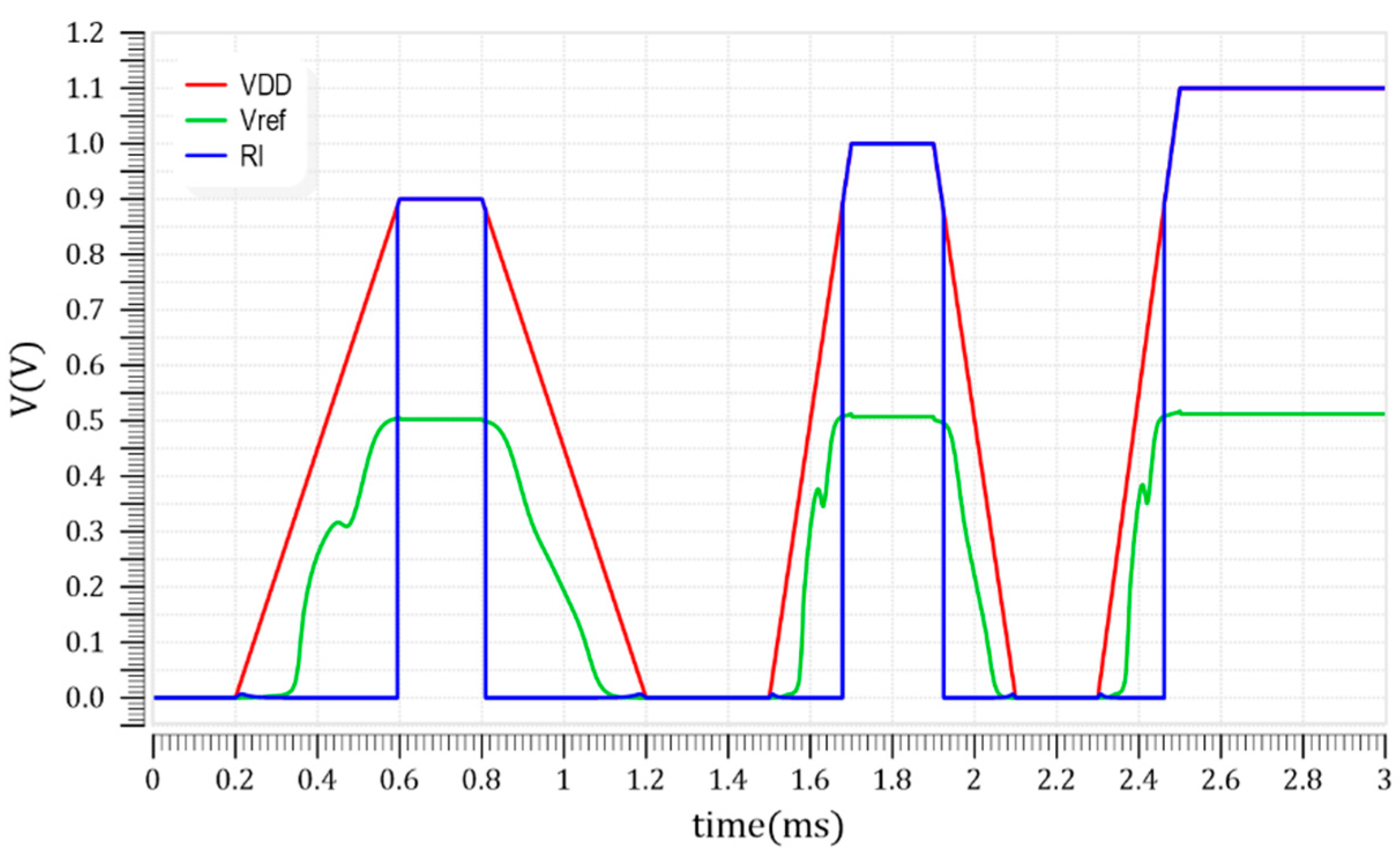
Post-layout simulation results depicted in
Figure 4 show the RI, the internal net voltages required for the comparison,
Vref voltage, and
VDD.
Vref takes unpredictable values before settling at the nominal value, as shown in
Figure 4a. It is also showing that the rising part of the waveform of the internal net
a1 is different than the falling part. The asymmetry is due to the internal capacitances and different internal resistance and switching times during powering up or down. The waveforms could be even more different in PVT corners and the correct detection even harder. Additionally, from corner simulations, it can be shown that the critical voltages not only take different final values but also can be of highly different waveforms with different rise and fall times and different settling times. Therefore, the two comparisons, one of
Vref with
a3, proportional to
VDD and the other of
Vref with
a1, guarantee the correct RI detection. The capacitor at node
a1 prevents the corresponding voltage from glitches and provides the necessary delay, during power-up and power-down. It must be noted that the
Vref also, is simulated with a capacitive load, about 8pF.
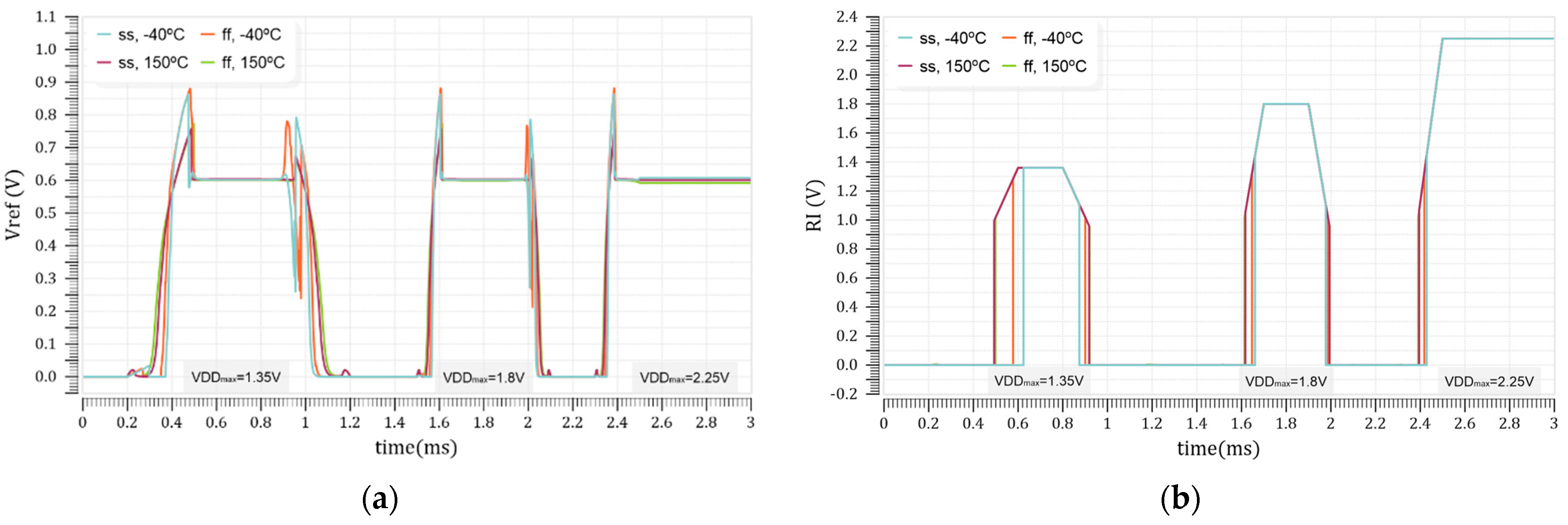
Post-layout corner simulations results are shown in
Figure 5. The RI detects clearly whether
Vref is in the nominal value. In
Figure 5b, the slopes of Ready-indication, close to the edges, are due to the
VDD value. In those cases,
VDD has not reached the final values and so, the Ready-indication has the same values, following
VDD ramp-up or ramp-down.
The corner analysis has been performed for the worst process corners, fast-fast (ff), and slow-slow (ss) and temperatures −40 °C and 150 °C.
3.2. RI Circuit for BGR#1 in 65 nm, 1 V Supply Voltage
The core of BGR presented in this subsection is of the same topology as that presented in
Section 3.1 and
Figure 3a. The difference now is that it has been designed and simulated in a 65 nm CMOS technology, with a 1 V supply voltage. Utilizing a 1 V, instead of 1.8 V supply voltage, results in a more complicated procedure to achieve the correct Ready-Indication, due to the limited voltage headroom in the transistors. Following the implementation proposed in
Section 3.1 with two comparators, the requested accuracy for RI is not achieved. Consequently, to avoid fault indication, one more comparison is required between
a1 and
a3, as shown in
Figure 6. The voltage
a1 is produced by the start-up circuit and
a3 is proportional to
VDD.
Simulation results presented in
Figure 7, show the
Vref voltage, as it is generated by the transitions of
VDD during power-up and power-down in different levels of
VDD. Additionally, the RI signal is depicted in the same figure.
Vref takes unsettled values before and after settling at the nominal value, alike to the results of the previous implementation. Therefore, the appropriate attention has been focused on these parts, considering that RI is detected clearly when
Vref is within the nominal value.
The precise detection of the RI becomes even harder in PVT corners, which constitute the final step of the procedure for the last settings to take place. Corner simulation results are shown in
Figure 8, where corner analysis has been performed for the process corners ss and ff, with
VDD equal to 1 V, supply voltage variation ±5%, and temperatures −40 °C and +120 °C.
3.3. Ready Indicator for BGR#2 in 65 nm, 1 V Supply Voltage
As mentioned above, in an attempt of further investigation of the RI concept, more BGR circuits with various features have been tested. The BGR#2 in this section is a two operational amplifiers topology, presented in [
8] and has been modified as shown in
Figure 9, to generate an RI signal. The BGR has been designed in a CMOS 65 nm, operating with a 1 V supply voltage.
In the present case, the contribution of only two comparators for the RI generation is sufficient. As has been previously reported, the first comparison occurs between
Vref and start-up (signal
a1 in
Figure 9). The second comparison is taken between
Vref and the output
nbias of the second operational amplifier in
Figure 9.
Simulation results that are presented in
Figure 10, show
Vref, as it is generated during the transitions of
VDD (1 V, ±10%), in comparison with the RI signal. PVT corner simulations results are shown in
Figure 11, where corner analysis has been performed for the process corners ss and ff, with
VDD equal to 1 V, supply voltage variation ±5%, and temperature −40 °C and +120 °C.
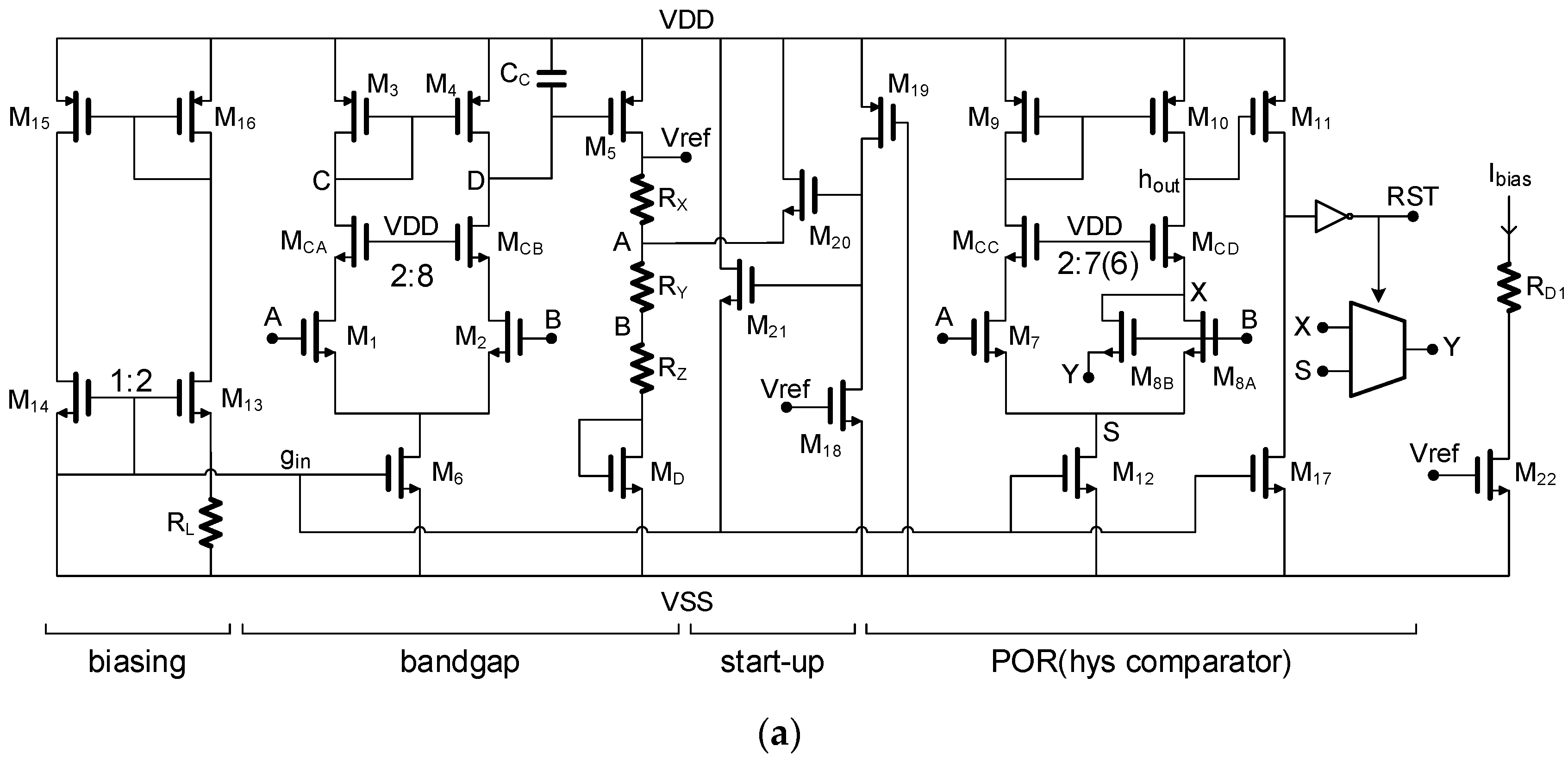
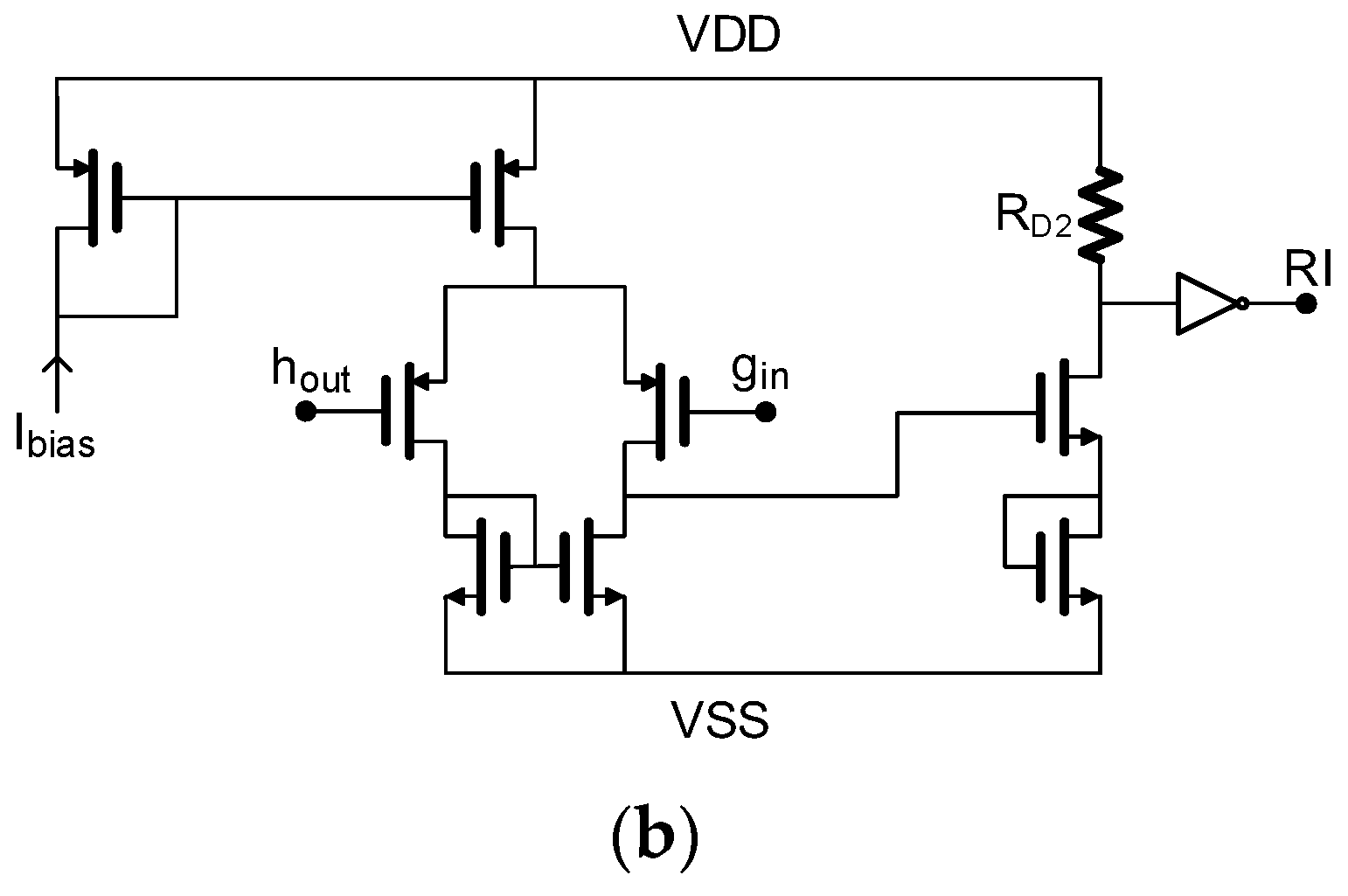
3.4. Ready Indicator for BGR#3 in 65 nm, 0.55 V Supply Voltage
A dedicated circuit for PoR with BGR is presented in [
3]. In this paper, a modified topology for higher accuracy in RI is proposed. The BGR#3 operation is based on MOS transistors only, without the contribution of bipolar transistors. It has been modified, as shown in
Figure 12, and has been designed and simulated in a 65 nm CMOS technology with 550 mV supply voltage. By reducing the value of the supply voltage to 550 mV, similarly to the previous circuits, the circumstances which should be taken under consideration for the achievement of precision become highly demanding. On the other hand, the most significant advantage of this circuit is the low power consumption, while the main disadvantage is the slow power-up and power-down time, which is expected in circuits with low current bias. Concerning the particular circuit, a relevant study for the suggested method has been conducted in [
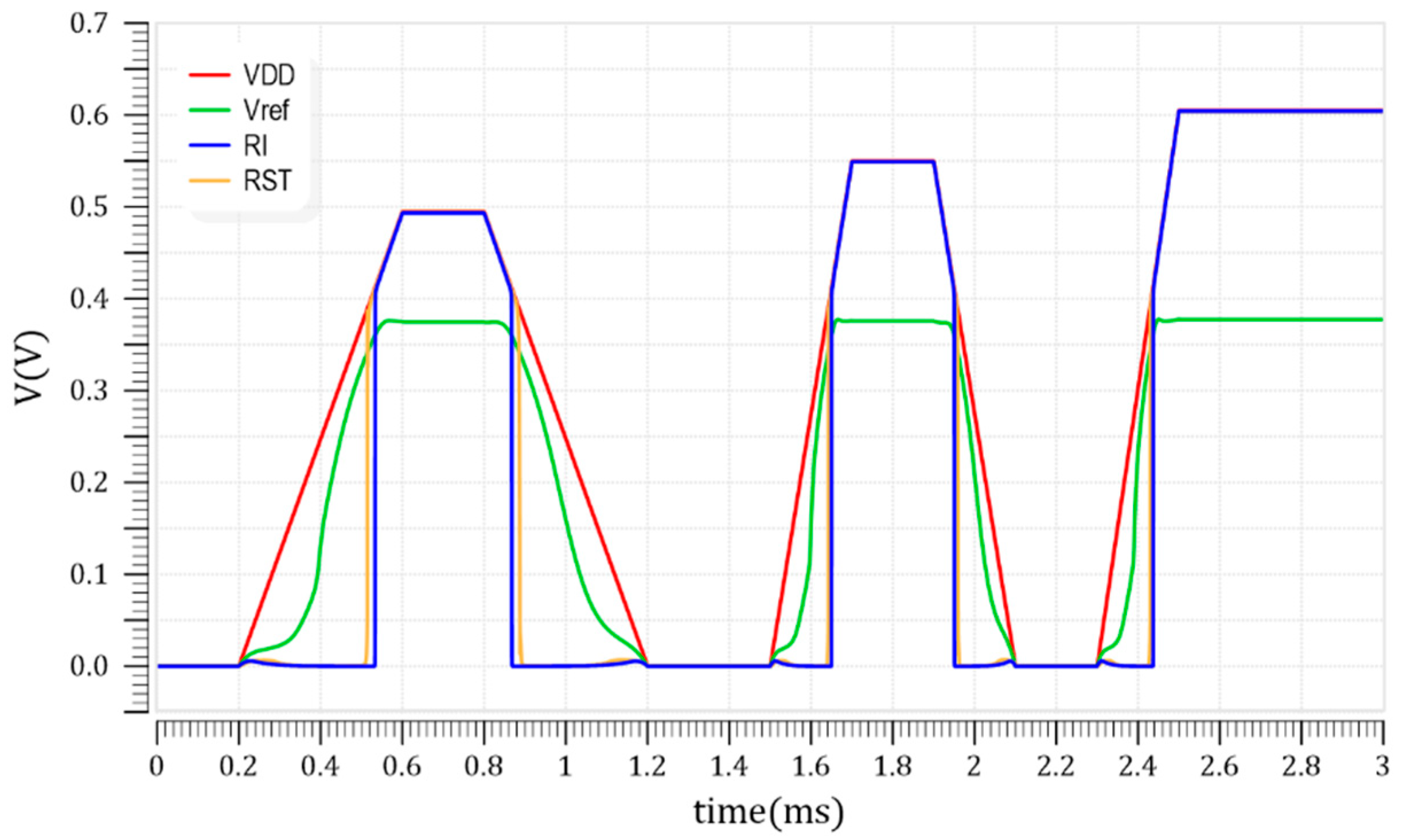
3], to address the issue of RI. The RST signal in that paper represents the expected RI signal. However, simulation results regarding the chosen technology depicted in
Figure 13, show that the RST output works while the
Vref is out of range. For more accurate operation a modified version of this circuit is proposed, by adding a comparison between
hout and
gin signals.
Simulation results of the proposed method on BGR#3, which are presented in
Figure 13, show improvement in RI compering with the already existing RST signal. The RI and
Vref voltages are depicted and generated during the transitions of
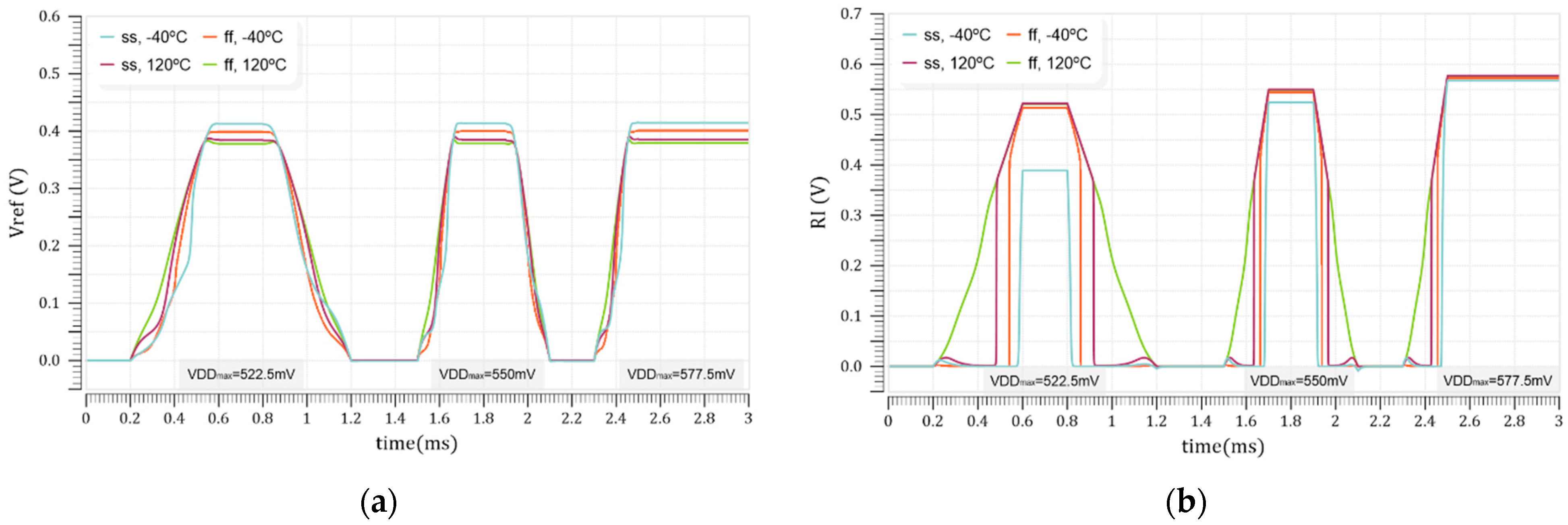
VDD (550 mV, ±10%). This BGR has been tested in corner analysis as well, showing correct operation and improved accuracy. PVT Corner simulations results are shown in
Figure 14, where corner analysis has been performed for the process corners ss and ff, with
VDD equal to 550 mV, supply voltage variation ±5%, and temperature −40 °C and +120 °C. From simulation results, it is shown that
Vref is not constant over variations of process corners. This behavior is reported, also, in the original work in [
3]. However, while
Vref is considered to operate at acceptable levels, RI also gives a correct positive signal.


