
Effect of Dielectric Thickness on Resistive Switching Polarity in TiN/Ti/HfO2/Pt Stacks

 ,
,  , , , , , , , and
Abstract
:1. Introduction
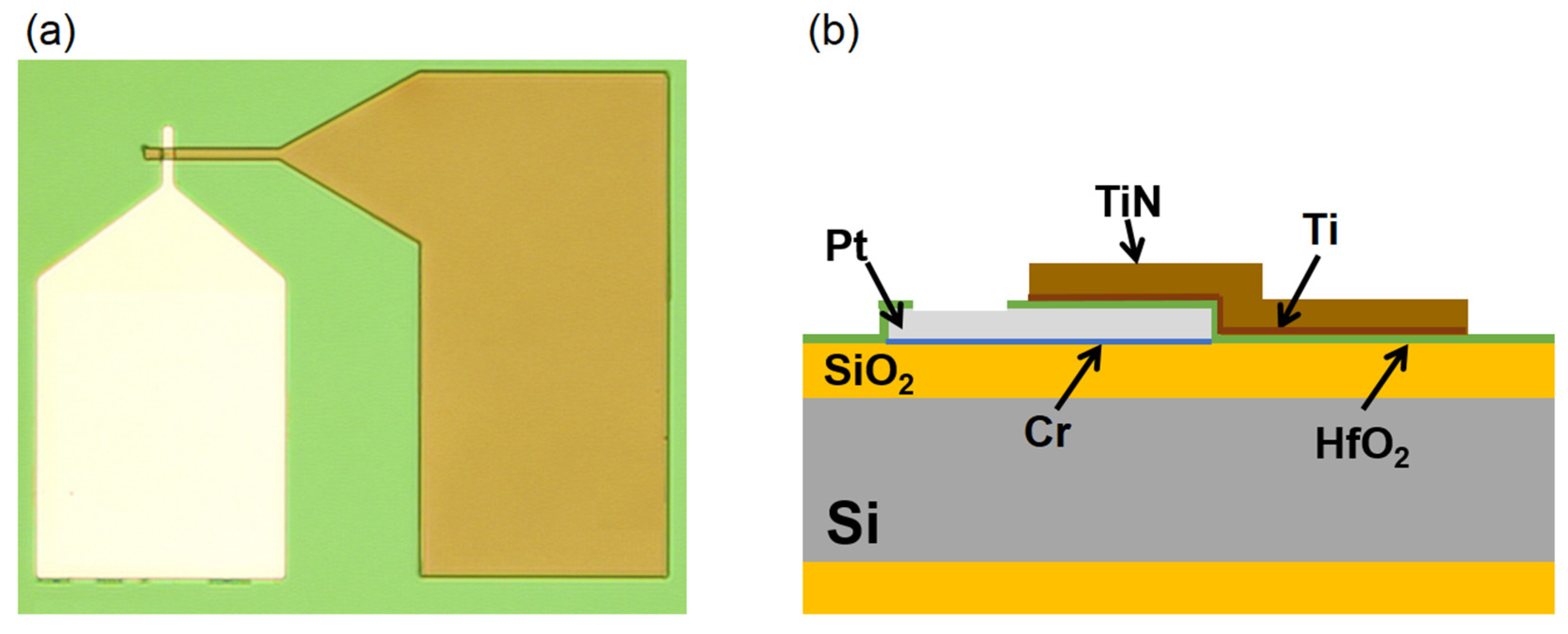
2. Materials and Methods
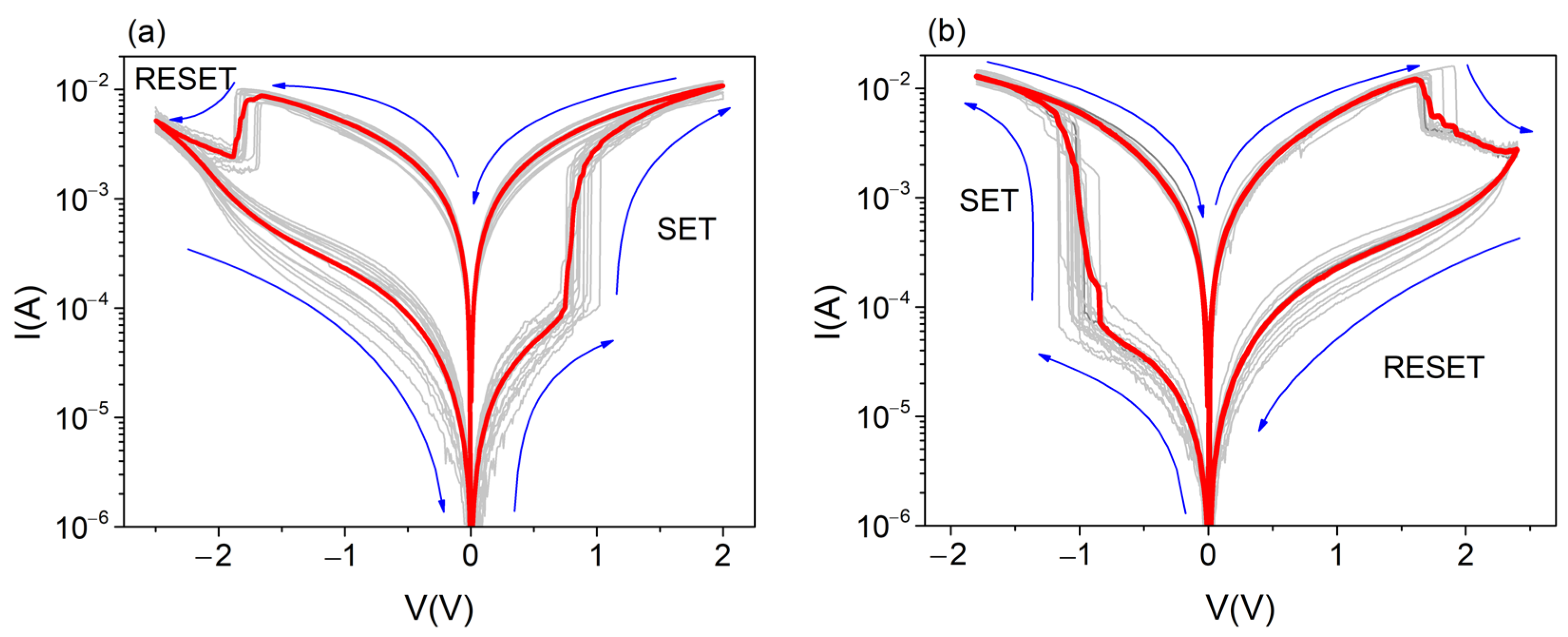
3. Results
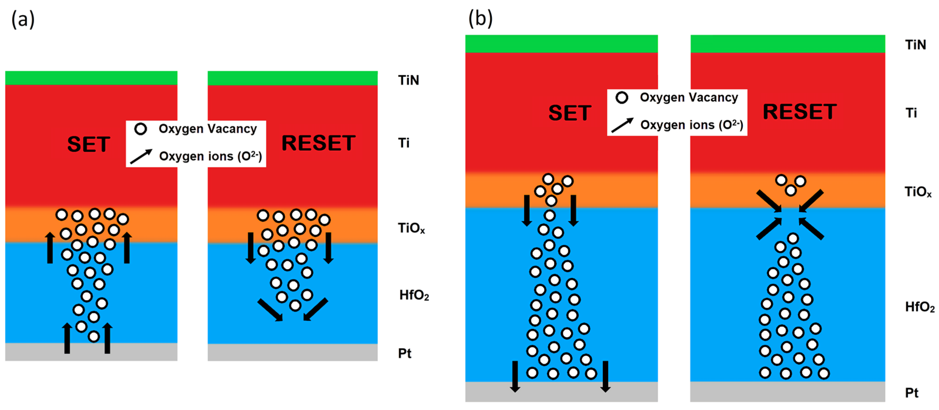
4. Discussion
5. Conclusions
Author Contributions
Funding
Conflicts of Interest
References
- Xu, N.; Gao, B.; Liu, L.; Sun, B.; Liu, X.; Han, R.; Kang, J.; Yu, B. A Unified Physical Model of Switching Behavior in Oxide-Based RRAM. In Proceedings of the 2008 Symposium on VLSI Technology, Honolulu, HI, USA, 17–19 June 2008; pp. 100–101. [Google Scholar]
- Huang, P.; Liu, X.Y.; Li, W.H.; Deng, Y.X.; Chen, B.; Lu, Y.; Gao, B.; Zeng, L.; Wei, K.L.; Du, G.; et al. A Physical Based Analytic Model of RRAM Operation for Circuit Simulation. In Proceedings of the 2012 IEDM, San Francisco, CA, USA, 10–13 December 2012. [Google Scholar]
- Lee, J.S.; Lee, S.; Noh, T.W. Resistive switching phenomena: A review of statistical physics approaches. Appl. Phys. Rev. 2015, 2, 031303. [Google Scholar] [CrossRef] [Green Version]
- Wouters, D.J.; Waser, R.; Wuttig, M. Phase-Change and Redox-Based Resistive Switching Memories. Proc. IEEE 2015, 103, 1274–1288. [Google Scholar] [CrossRef]
- Lanza, M. A Review on Resistive Switching in High-k Dielectrics: A Nanoscale Point of View Using Conductive Atomic Force Microscope. Materials 2014, 7, 2155–2182. [Google Scholar] [CrossRef]
- Ye, C.; Wu, J.; He, G.; Zhang, J.; Deng, T.; He, P.; Wang, H. Physical Mechanism and Performance Factors of Metal Oxide Based Resistive Switching Memory: A Review. J. Mater. Sci. Technol. 2016, 32, 1–11. [Google Scholar] [CrossRef]
- Cavallini, M.; Hemmatian, Z.; Riminucci, A.; Prezioso, M.; Morandi, V.; Murgia, M. Regenerable Resistive Switching in Silicon Oxide Based Nanojunctions. Adv. Mater. 2012, 24, 1197–1201. [Google Scholar] [CrossRef] [PubMed]
- Chen, W.; Lu, W.; Long, B.; Li, Y.; Gilmer, D.; Bersuker, G.; Bhunia, S.; Jha, R. Switching characteristics of W/Zr/HfO2/TiN ReRAM devices for multi-level cell non-volatile memory applications. Semicond. Sci. Technol. 2015, 30, 075002. [Google Scholar] [CrossRef]
- Dueñas, S.; Castán, H.; García, H.; Miranda, E.; Gonzalez, M.; Campabadal, F. Study of the admittance hysteresis cycles in TiN/Ti/HfO2/W-based RRAM devices. Microelectron. Eng. 2017, 178, 30–33. [Google Scholar] [CrossRef]
- Rodriguez-Fernandez, A.; Cagli, C.; Perniola, L.; Miranda, E.; Suñé, J. Characterization of HfO2-based devices with indication of second order memristor effects. Microelectron. Eng. 2018, 195, 101–106. [Google Scholar] [CrossRef] [Green Version]
- Niinistö, J.; Kukli, K.; Heikkilä, M.; Ritala, M.; Leskelä, M. Atomic Layer Deposition of High-kOxides of the Group 4 Metals for Memory Applications. Adv. Eng. Mater. 2009, 11, 223–234. [Google Scholar] [CrossRef]
- Ossorio, O.G.; Poblador, S.; Vinuesa, G.; Duenas, S.; Castan, H.; Maestro-Izquierdo, M.; Bargallo, M.G.; Campabadal, F. Single and Complex Devices on Three Topological Configurations of HfO2 Based RRAM. In Proceedings of the 2020 IEEE LAEDC, San José, Costa Rica, 25–28 February 2020; pp. 1–4. [Google Scholar]
- Makarov, A.; Sverdlov, V.; Selberherr, S. Stochastic model of the resistive switching mechanism in bipolar resistive random-access memory: Monte Carlo simulations. J. Vac. Sci. Technol. B Nanotechnol. Microelectron. Mater. Process. Meas. Phenom. 2011, 29, 01AD03. [Google Scholar] [CrossRef]
- Feng, W.; Shima, H.; Ohmori, K.; Akinaga, H. Investigation of switching mechanism in HfOx-ReRAM under low power and conventional operation modes. Sci. Rep. 2016, 6, 39510. [Google Scholar] [CrossRef] [Green Version]
- Kwak, J.S.; Do, Y.H.; Bae, Y.C.; Im, H.S.; Yoo, J.H.; Sung, M.G.; Hwang, Y.T.; Hong, J.P. Roles of interfacial TiOxN1−x layer and TiN electrode on bipolar resistive switching in TiN/TiO2/TiN frameworks. Appl. Phys. Lett. 2010, 96, 223502. [Google Scholar] [CrossRef]
- Do, Y.H.; Kwak, J.S.; Bae, Y.C.; Lee, J.H.; Kim, Y.; Im, H.; Hong, J.P. TiN electrode-induced bipolar resistive switching of TiO2 thin films. Curr. Appl. Phys. 2010, 10, e71–e74. [Google Scholar] [CrossRef]
- Kim, K.M.; Kim, G.H.; Song, S.J.; Seok, J.Y.; Lee, M.H.; Yoon, J.H.; Hwang, C.S. Electrically configurable electroforming and bipolar resistive switching in Pt/TiO2/Pt structures. Nanotechnology 2010, 21, 305203. [Google Scholar] [CrossRef] [PubMed]
- Bae, Y.C.; Lee, A.R.; Bin Lee, J.; Koo, J.H.; Kwon, K.C.; Park, J.G.; Im, H.S.; Hong, J.P. Oxygen Ion Drift-Induced Complementary Resistive Switching in Homo TiOx/TiOy/TiOxand Hetero TiOx/TiON/TiOxTriple Multilayer Frameworks. Adv. Funct. Mater. 2011, 22, 709–716. [Google Scholar] [CrossRef]
- Biju, K.P. Resistive switching characteristics of thermally oxidized TiN thin films. AIP Conf. Proc. 2018, 1942, 060023. [Google Scholar] [CrossRef]
- Yan, X.B.; Xia, Y.D.; Xu, H.N.; Gao, X.; Li, H.T.; Li, R.; Yin, J.; Liu, Z.G. Effects of the electroforming polarity on bipolar resistive switching characteristics of SrTiO3−δ films. Appl. Phys. Lett. 2010, 97, 112101. [Google Scholar] [CrossRef]
- Shibuya, K.; Dittmann, R.; Mi, S.; Waser, R. Impact of Defect Distribution on Resistive Switching Characteristics of Sr2TiO4Thin Films. Adv. Mater. 2010, 22, 411–414. [Google Scholar] [CrossRef]
- Zhu, H.X.; Huo, J.Q.; Qiu, X.Y.; Zhang, Y.Y.; Wang, R.X.; Chen, Y.; Wong, C.M.; Yau, H.M.; Dai, J.Y. Thickness-Dependent Bipolar Resistive Switching Behaviors of NiOx Films. Mater. Sci. Forum 2016, 847, 131–136. [Google Scholar] [CrossRef]
- Biju, K.P.; Liu, X.; Siddik, M.; Kim, S.; Shin, J.; Kim, I.; Ignatiev, A.; Hwang, H. Resistive switching characteristics and mechanism of thermally grown WOx thin films. J. Appl. Phys. 2011, 110, 64505. [Google Scholar] [CrossRef]
- Biju, K.P.; Liu, X.; Kim, S.; Jung, S.; Park, J.; Hwang, H. Coexistence of filamentary and homogeneous resistive switching in graded WO x thin films. Phys. Status Solidi Rapid Res. Lett. 2011, 5, 89–91. [Google Scholar] [CrossRef]
- Zhang, H.Z.; Ang, D.S.; Gu, C.J.; Yew, K.S.; Wang, X.P.; Lo, G.Q. Role of interfacial layer on complementary resistive switching in the TiN/HfOx/TiN resistive memory device. Appl. Phys. Lett. 2014, 105, 222106. [Google Scholar] [CrossRef]
- Brivio, S.; Frascaroli, J.; Spiga, S. Role of metal-oxide interfaces in the multiple resistance switching regimes of Pt/HfO2/TiN devices. Appl. Phys. Lett. 2015, 107, 023504. [Google Scholar] [CrossRef]
- Petzold, S.; Miranda, E.; Sharath, S.U.; Muñoz-Gorriz, J.; Vogel, T.; Piros, E.; Kaiser, N.; Eilhardt, R.; Zintler, A.; Molina-Luna, L.; et al. Analysis and simulation of the multiple resistive switching modes occurring in HfOx-based resistive random-access memories using memdiodes. J. Appl. Phys. 2019, 125, 234503. [Google Scholar] [CrossRef] [Green Version]
- Goux, L.; Chen, Y.-Y.; Pantisano, L.; Wang, X.-P.; Groeseneken, G.; Jurczak, M.; Wouters, D.J. On the Gradual Unipolar and Bipolar Resistive Switching of TiN\HfO2\Pt Memory Systems. Electrochem. Solid State Lett. 2010, 13, G54–G56. [Google Scholar] [CrossRef]
- Goux, L.; Wang, X.P.; Chen, Y.Y.; Pantisano, L.; Jossart, N.; Govoreanu, B.; Kittl, J.A.; Jurczak, M.; Altimime, L.; Wouters, D.J. Roles and Effects of TiN and Pt Electrodes in Resistive-Switching HfO2 Systems. Electrochem. Solid State Lett. 2011, 14, H244–H246. [Google Scholar] [CrossRef]
- Goux, L.; Czarnecki, P.; Chen, Y.Y.; Pantisano, L.; Wang, X.P.; Degraeve, R.; Govoreanu, B.; Jurczak, M.; Wouters, D.J.; Altimime, L. Evidence of oxygen-mediated resistive-switching mechanism in TiN\HfO2\Pt cells. Appl. Phys. Lett. 2010, 97, 243509. [Google Scholar] [CrossRef]
- Giovinazzo, C.; Sandrini, J.; Shahrabi, E.; Celik, O.T.; Leblebici, Y.; Ricciardi, C. Analog Control of Retainable Resistance Multistates in HfO2 Resistive-Switching Random Access Memories (ReRAMs). ACS Appl. Electron. Mater. 2019, 1, 900–909. [Google Scholar] [CrossRef]
- Wang, Z.; Jiang, H.; Jang, M.H.; Lin, P.; Ribbe, A.; Xia, Q.; Yang, J.J. Electrochemical metallization switching with a platinum group metal in different oxides. Nanoscale 2016, 8, 14023–14030. [Google Scholar] [CrossRef]
- Raffone, F.; Cicero, G. Does platinum play a role in the resistance switching of ZnO nanowire-based devices? Solid State Ion. 2017, 299, 93–95. [Google Scholar] [CrossRef]
- Lee, H.Y.; Chen, Y.S.; Wu, T.Y.; Chen, F.; Wang, C.C.; Tzeng, P.J.; Tsai, M.-J.; Lien, C.-H. Low-Power and Nanosecond Switching in Robust Hafnium Oxide Resistive Memory with a Thin Ti Cap. IEEE Electron Device Lett. 2009, 31, 44–46. [Google Scholar] [CrossRef]
- Fang, Z.; Wang, X.P.; Sohn, J.; Bin Weng, B.; Zhang, Z.P.; Chen, Z.X.; Tang, Y.Z.; Lo, G.-Q.; Provine, J.; Wong, S.S.; et al. The Role of Ti Capping Layer in HfOx-Based RRAM Devices. IEEE Electron Device Lett. 2014, 35, 912–914. [Google Scholar] [CrossRef]
- Gao, B.; Yu, S.; Xu, N.; Liu, L.; Sun, B.; Liu, X.; Han, R.; Kang, J.; Yu, B.; Wang, Y. Oxide-Based RRAM Switching Mechanism: A New Ion-Transport-Recombination Model. In Proceedings of the IEDM, San Francisco, CA, USA, 15–17 December 2008; pp. 1–4. [Google Scholar]
- Dirkmann, S.; Kaiser, J.; Wenger, C.; Mussenbrock, T. Filament Growth and Resistive Switching in Hafnium Oxide Memristive Devices. ACS Appl. Mater. Interfaces 2018, 10, 14857–14868. [Google Scholar] [CrossRef] [PubMed]
- Kinoshita, K.; Tsunoda, K.; Sato, Y.; Noshiro, H.; Yagaki, S.; Aoki, M.; Sugiyama, Y. Reduction in the reset current in a resistive random-access memory consisting of NiOx brought about by reducing a parasitic capacitance. Appl. Phys. Lett. 2008, 93, 033506. [Google Scholar] [CrossRef]
- Gilmer, D.C.; Bersuker, G.; Park, H.-Y.; Park, C.; Butcher, B.; Wang, W.; Kirsch, P.D.; Jammy, R. Effects of RRAM Stack Configuration on Forming Voltage and Current Overshoot. In Proceedings of the 3rd IEEE IMW, Monterey, CA, USA, 22–25 May 2011. [Google Scholar]
- Bersuker, G.; Gilmer, D.C.; Veksler, D.; Kirsch, P.; Vandelli, L.; Padovani, A.; Larcher, L.; McKenna, K.; Shluger, A.; Iglesias, V.; et al. Metal oxide resistive memory switching mechanism based on conductive filament properties. J. Appl. Phys. 2011, 110, 124518. [Google Scholar] [CrossRef]
- Wan, H.J.; Zhou, P.; Ye, L.; Lin, Y.Y.; Tang, T.A.; Wu, H.M.; Chi, M.H. In Situ Observation of Compliance-Current Overshoot and Its Effect on Resistive Switching. IEEE Electron. Device Lett. 2010, 31, 246–248. [Google Scholar] [CrossRef]
- Hardtdegen, A.; Zhang, H.; Hoffmann-Eifert, S. Tuning the Performance of Pt/HfO2/Ti/Pt ReRAM Devices Obtained from Plasma-Enhanced Atomic Layer Deposition for HfO2 Thin Films. ECS Trans. 2016, 75, 177–184. [Google Scholar] [CrossRef]
- Cao, K.; van Lent, R.; Kleyn, A.W.; Kurahashi, M.; Juurlink, L.B.F. Steps on Pt stereodynamically filter sticking of O2. Proc. Natl. Acad. Sci. USA 2019, 116, 13862–13866. [Google Scholar] [CrossRef] [Green Version]
- Gutiérrez-González, A.; Beck, R.D. Unraveling the complexity of oxygen reactions on Pt surfaces. Proc. Natl. Acad. Sci. USA 2019, 116, 13727–13728. [Google Scholar] [CrossRef] [Green Version]
- Nakajima, R.; Azuma, A.; Yoshida, H.; Shimizu, T.; Ito, T.; Shingubara, S. Hf layer thickness dependence of resistive switching characteristics of Ti/Hf/HfO2/Au resistive random access memory device. Jpn. J. Appl. Phys. 2018, 57, 06HD06. [Google Scholar] [CrossRef] [Green Version]
- Hsieh, C.-C.; Roy, A.; Rai, A.; Chang, Y.-F.; Banerjee, S.K. Characteristics and mechanism study of cerium oxide based random access memories. Appl. Phys. Lett. 2015, 106, 173108. [Google Scholar] [CrossRef]
- Hong, S.K.; Kim, J.E.; Kim, S.O.; Choi, S.-Y.; Cho, B.J. Flexible Resistive Switching Memory Device Based on Graphene Oxide. IEEE Electron. Device Lett. 2010, 31, 1005–1007. [Google Scholar] [CrossRef]
- Govoreanu, B.; Kar, G.; Chen, Y.-Y.; Paraschiv, V.; Kubicek, S.; Fantini, A.; Radu, I.; Goux, L.; Clima, S.; Degraeve, R.; et al. 1010 nm2 Hf/HfOx Crossbar Resistive RAM with Excellent Performance, Reliability and Low-Energy Operation. In Proceedings of the International Electron Devices Meeting, Washington, DC, USA, 5–7 December 2011. [Google Scholar]
- Lee, H.Y.; Chen, P.S.; Wu, T.Y.; Chen, Y.S.; Wang, C.C.; Tzeng, P.J.; Lin, C.H.; Chen, F.; Lien, C.H.; Tasi, M.J. Low Power and High-Speed Bipolar Switching with a Thin Reactive Ti Buffer Layer in Robust HfO2 Based RRAM. In Proceedings of the 2008 IEEE International Electron Devices Meeting, San Francisco, CA, USA, 14–17 December 2008. [Google Scholar]
- Bruchhaus, R.; Hermes, C.; Waser, R. Memristive Switches with Two Switching Polarities in a Forming Free Device Structure. MRS Proc. 2011, 1337, 803. [Google Scholar] [CrossRef]
- Jeong, D.S.; Choi, B.J.; Hwang, C.S. Electroforming Processes in Metal Oxide Resistive-Switching Cells. In Resistive Switching; Ielmini, D., Waser, R., Eds.; John Wiley & Sons, Ltd.: Hoboken, NJ, USA, 2016; pp. 289–316. [Google Scholar]
- McKenna, K.P. Optimal stoichiometry for nucleation and growth of conductive filaments in HfOx. Model. Simul. Mater. Sci. Eng. 2014, 22, 025001. [Google Scholar] [CrossRef] [Green Version]
- He, S.; Hao, A.; Qin, N.; Bao, D. Unipolar resistive switching properties of Pr-doped ZnO thin films. Ceram. Int. 2017, 43, S474–S480. [Google Scholar] [CrossRef]


Publisher’s Note: MDPI stays neutral with regard to jurisdictional claims in published maps and institutional affiliations. |
© 2022 by the authors. Licensee MDPI, Basel, Switzerland. This article is an open access article distributed under the terms and conditions of the Creative Commons Attribution (CC BY) license (https://creativecommons.org/licenses/by/4.0/).
Share and Cite
Vinuesa, G.; García, H.; González, M.B.; Kalam, K.; Zabala, M.; Tarre, A.; Kukli, K.; Tamm, A.; Campabadal, F.; Jiménez, J.; et al. Effect of Dielectric Thickness on Resistive Switching Polarity in TiN/Ti/HfO2/Pt Stacks. Electronics 2022, 11, 479. https://doi.org/10.3390/electronics11030479
Vinuesa G, García H, González MB, Kalam K, Zabala M, Tarre A, Kukli K, Tamm A, Campabadal F, Jiménez J, et al. Effect of Dielectric Thickness on Resistive Switching Polarity in TiN/Ti/HfO2/Pt Stacks. Electronics. 2022; 11(3):479. https://doi.org/10.3390/electronics11030479
Chicago/Turabian StyleVinuesa, Guillermo, Héctor García, Mireia B. González, Kristjan Kalam, Miguel Zabala, Aivar Tarre, Kaupo Kukli, Aile Tamm, Francesca Campabadal, Juan Jiménez, and et al. 2022. "Effect of Dielectric Thickness on Resistive Switching Polarity in TiN/Ti/HfO2/Pt Stacks" Electronics 11, no. 3: 479. https://doi.org/10.3390/electronics11030479
APA StyleVinuesa, G., García, H., González, M. B., Kalam, K., Zabala, M., Tarre, A., Kukli, K., Tamm, A., Campabadal, F., Jiménez, J., Castán, H., & Dueñas, S. (2022). Effect of Dielectric Thickness on Resistive Switching Polarity in TiN/Ti/HfO2/Pt Stacks. Electronics, 11(3), 479. https://doi.org/10.3390/electronics11030479