Article

A Vacuum Transistor Based on Field-Assisted Thermionic Emission from a Multiwalled Carbon Nanotube

Key Laboratory for the Physics and Chemistry of Nanodevices, School of Electronics, Peking University, Beijing 100871, China
*
Author to whom correspondence should be addressed.
These authors contributed equally to this work.
Electronics 2022, 11(3), 399; https://doi.org/10.3390/electronics11030399
Submission received: 28 December 2021 / Revised: 23 January 2022 / Accepted: 25 January 2022 / Published: 28 January 2022
(This article belongs to the Special Issue High-Frequency Vacuum Electron Devices)

Abstract

:
Vacuum triodes have been scaled down to the microscale on a chip by microfabrication technologies to be vacuum transistors. Most of the reported devices are based on field electron emission, which suffer from the problems of unstable electron emission, poor uniformity, and high requirement for operating vacuum. Here, to overcome these problems, a vacuum transistor based on Field-Assisted thermionic emission from individual carbon nanotubes is proposed and fabricated using microfabrication technologies. The carbon nanotube vacuum transistor exhibits an ON/OFF current ratio as high as 104 and a subthreshold slope of ~4 V·dec−1. The gate controllability is found to be strongly dependent on the distance between the collector electrodes and electron emitter, and a device with the distance of 1.5 μm shows a better gate controllability than that with the distance of 0.5 μm. Benefiting from Field-Assisted thermionic emission mechanism, electric field required in our devices is about one order of magnitude smaller than that in the devices based on field electron emission, and the surface of the emitters shows much less gas molecule absorption than cold field emitters. These are expected to be helpful for improving the stability and uniformity of the devices.

1. Introduction

Vacuum tubes emerged in the early 20th century and were the central of the original electronic devices [1]. However, solid-state devices took over their roles in most areas in the past 60 years because of the advantages of integrability, miniaturization, lower power consumption, reduced costs, etc. Recently, vacuum transistors, miniature vacuum triodes fabricated on a chip by microfabrication technologies, have rekindled many researchers’ interest because of the advantages associated with vacuum devices. Vacuum as a medium for electron transport is more immune to radiation damage than conventional semiconductors. Thus, vacuum devices are stable under harsh environment [2]. Furthermore, the velocity of electrons transporting in a vacuum is higher than that in semiconductors, because electrons in a vacuum are free of scattering with a theoretical velocity approaching 3 × 10⁸ m·s−1. Meanwhile, vacuum devices are more reliable and efficient than solid-state devices for high-power and high-frequency devices [3]. Up to now, the functionality of vacuum devices has been demonstrated in a wide range of applications, such as deep space communications [2], premier sound system [4], high-frequency and high-power devices [5], terahertz laser [6] and military defense. Combining vacuum triodes and microfabrication technologies leads to the creation of a new area called “vacuum transistors”, which is expected to possess the advantages of both conventional vacuum devices and solid-state devices, such as high carrier velocity, reliable performances in high temperature and extreme environment, miniaturization and easy integration [7].
In recent years, as many researchers have put their efforts into this field, various vacuum transistors fabricated by microfabrication technologies have been reported [7,8,9,10,11,12,13,14,15,16,17]. Miniaturization of vacuum triodes can lead to higher integration, lower working voltages and lower power consumption. For instance, Shruti Nirantar et al. proposed a semiconductor−free field emission nanoscale channel transistor, where the gap between field emission electrodes is about 35 nm [8]. As the gap is less than the mean free path of electrons in the air pressure (~60 nm), electrons encounter fewer collisions with air molecules even in air pressure [9]. Jin-Woo Han et al. fabricated a surround gate nanoscale vacuum channel transistor by using ion implantation and ion etching, achieving a low operating voltage (<5 V) and good immunity to various types of radiation [10]. In addition, Jin-Woo Han et al. reported vertical surround-gate nanoscale vacuum transistors that can be fabricated on silicon carbide wafers with stable electron emission and long-term stability of emitters [7]. The extended gate structure enhances the gate-to-emitter controllability and reduces the leakage current. A fully integrated, on-chip vacuum transistor based on field emission from carbon nanotubes via silicon micromachining processes was proposed by C. Bower et al. [11], achieving high frequency (10 GHz) and low control voltage (50–100 V) operation but still suffering from complex fabrication processes and inadequate emission stability and reliability of the carbon nanotubes emitters.
Intense research over the past decades has mainly focused on field emission vacuum transistors. Nevertheless, an intense local electric field with a typical magnitude of several volts per nanometer is required to induce field emission, which makes sharp tips preferred for field emitters with a large field enhancement factor and field emission quite sensitive to the microstructures of emitters. In addition, the electrons can ionize ambient gases such as oxygen and nitrogen with an enough high kinetic energy. Being accelerated along the electric field due to the cathode voltage, the positive ions will collide with the emitters and cause mechanical degradation of emitters leading to an unstable electron emission [8]. Moreover, field emission is quite sensitive to the absorption of ambient molecules onto emitters, which can change the work function of the emitters [18]. Therefore, an ultrahigh vacuum is required for stable field emission. As a result, field emission vacuum transistors still encounter the problems of unstable electron emission, poor uniformity and repeatability, and complex processing. Compared to field emission, thermionic electron emission is much less sensitive to the microstructures of the emitter and molecule absorption, indicating much more controllable and stable electron emission. A few years ago, a graphene−based vacuum transistor (GVT) was demonstrated by employing an electrically biased graphene as the thermionic electron emitter [19]. The GVT exhibits promising performances in several aspects, such as high ON/OFF ratio, small subthreshold slope, and low operating voltages. Importantly, this device provides a feasible way to achieving vacuum channel transistors based on thermionic electron emission. However, the GVT shows disadvantages of large leakage current and a high-power consumption.
In this paper, we report the scaling down of vacuum triodes to the microscale on a chip by employing a single Joule−heated multiwalled carbon nanotube (CNT) as the filament for thermionic electron emission. The CNT-based vacuum transistor (CVT) can be switched by tuning the bias voltage applied to the heavily doped silicon substrate (bottom gate) with an ON/OFF current ratio up to 104, and a subthreshold slope of ~4 V·dec−1. We also study the dependence of gate controllability on the distance between collector electrodes and emitter. The simulation of the electric field at the surface of CNTs indicates that the electric field in our devices is about one order of magnitude smaller than that in the devices based on field electron emission.

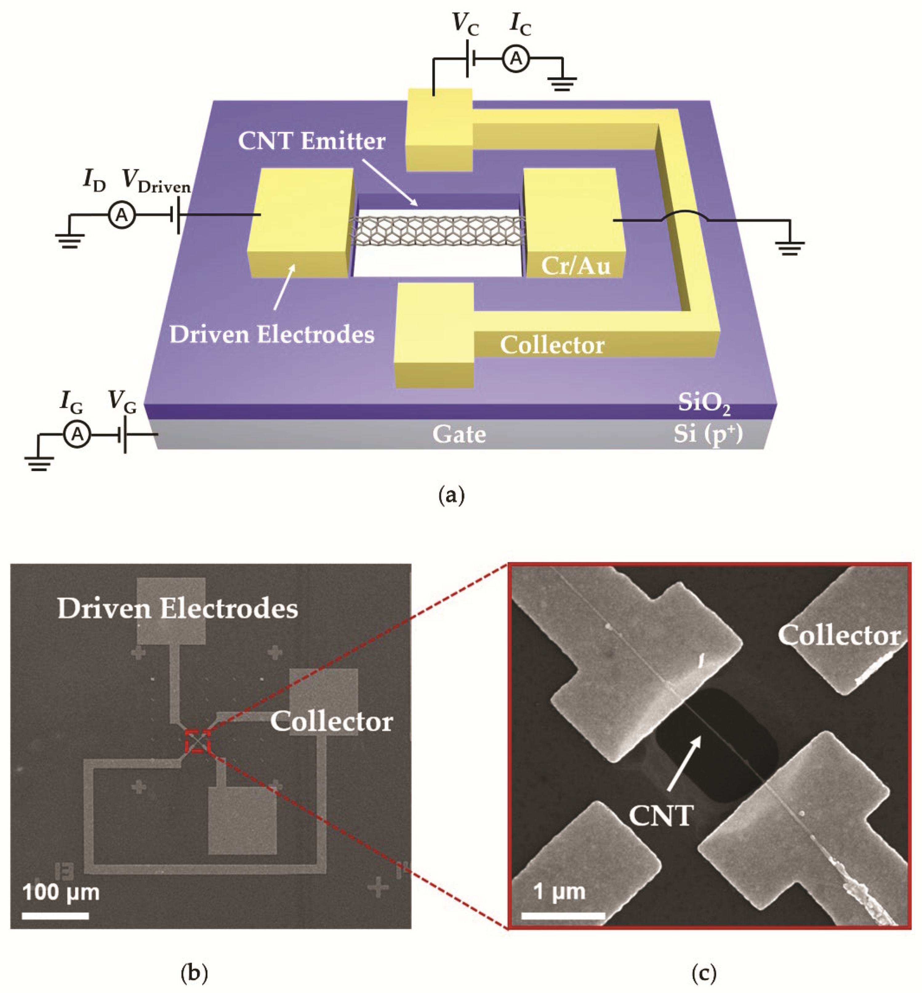
2. Materials and Methods

The schematic structure of a CVT is shown in Figure 1a, where a multiwalled CNT, acting as a filament, is freely suspended above a heavily doped Si substrate and pressed between Au/Cr electrodes. To excite thermionic electron emission from the CNT, a bias voltage (VDriven) is applied to the suspended CNT, thus an electrical current (ID) will pass through and heat it by self−Joule heating. A pair of Au/Cr electrodes with a collecting voltage (VC) of 50 V are beside the CNT acting as the collector electrodes. As demonstrated in pervious works, thermionic electrons emit from a Joule−heated carbon nanotube while a bias voltage applied to it is larger than a threshold value, and the emission current increases exponentially with the bias voltage [20,21,22]. To switch emission current collected by the collector electrodes (IC), the heavily doped Si substrate underneath the suspended CNT works as the gate electrode with a bias voltage (VG) of −10–40 V. Figure 1b shows a scanning electron microscope (SEM) image of a CVT, and the magnified SEM image of the center area of the CVT is shown in Figure 1c, in which the distance between collector electrodes and electron emitter is approximately 1.5 μm.
CNT-based vacuum transistors are fabricated on SiO2/Si wafer substrates by microfabrication technologies, where the SiO2 layer thickness is 300 nm. The metallic multiwalled carbon nanotubes fabricated by arc discharge with a smooth surface and a perfect structure are dispersed on the substrate in alcohol solution. A proper carbon nanotube is selected first for device fabrication via SEM observation. The average diameter of selected carbon nanotubes is about 10 nm. Next, a pair of Au/Cr (80 nm/10 nm) driven electrodes and collector electrodes are fabricated by electron-beam lithography (EBL), electron-beam evaporator deposition, and a standard lift-off process, successively. To enhance the electron emission from a Joule−heated CNT [23,24], the SiO2 layer underneath CNT must be removed by chemical etching to make the multiwalled CNT suspended over the Si substrate. A layer of polymethyl methacrylate (PMMA) is first used as a mask and the area for etching is defined by EBL. Second, the sample is plunged into buffered hydrofluoric acid for 330 s to remove the SiO2 layer. After washing off the PMMA mask in acetone and drying the sample in hot isopropanol, a CNT-based vacuum transistor as shown in Figure 1 is finally obtained.

3. Results and Discussion

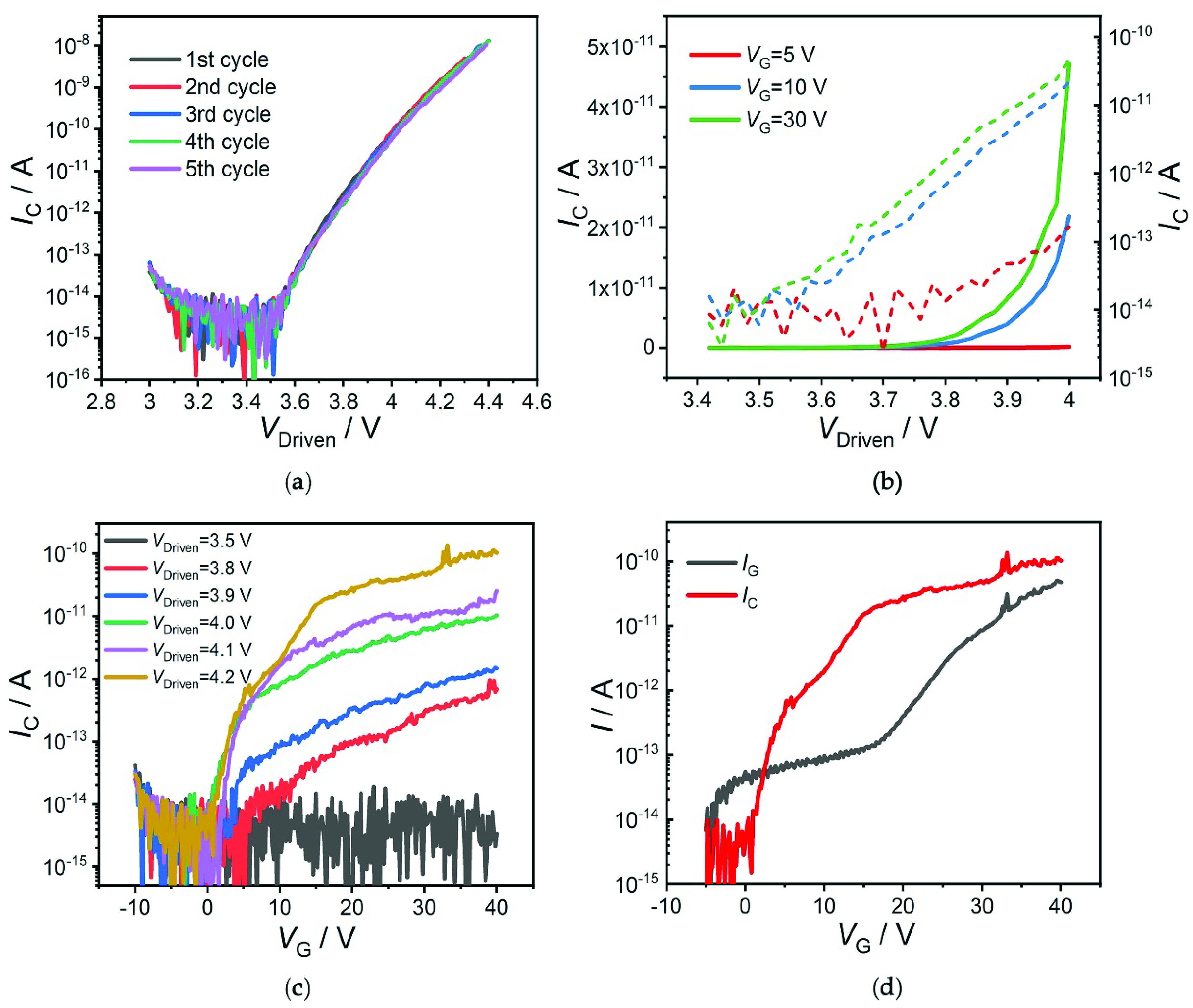
3.1. Thermionic Emission from a Multiwalled Carbon Nanotube

The performances of CVTs are measured on a probe station at room temperature with the vacuum level of about 1 × 10⁻² Pa utilizing a Keithley 4200 semiconductor characterization system. The emission current of a multiwalled CNT electron emitter is measured repeatedly with collector electrodes applied with 50 V and gate electrode vacant. The device exhibits repeatable electron emission for five different measurements, as shown in Figure 2a. There is no emission current collected by collector electrode until VDriven is larger than ~3.6 V, and the maximum emission current can reach up to 10 nA when VDriven is ~4.4 V. It can be seen from Figure 2a that IC increases exponentially with VDriven, in good agreement with previous observation of thermionic emission from a suspended CNT [20,21,22]. As the collecting voltage is fixed at 50 V and thus electric field at the surface of the CNT is almost unchanged during the measurements, electron emission is not governed by electric field. The electron emission from a Joule−heated CNT is attributed to thermionic emission mechanism with non−thermal equilibrium electron distribution [20,21].

3.2. Output Characteristic and Transfer Characteristic of a CNT-based Vacuum Transistor

Figure 2b shows the output characteristic (ICVDriven curves) of a CVT at different gate voltages of 5 V, 10 V, 30 V, respectively. It can be seen from the curves plotted in exponential scale that the emission current increases exponentially with VDriven and gate voltage also has a significant influence on emission current, implying a gate controllability. The transfer characteristic (ICVG curves) of a CVT with distance between collector electrode and emitter (D) of 1.5 μm under different driven voltages (VDriven) applied to the multiwalled CNT is shown in Figure 2c when the collecting voltage is fixed at 50 V. It can be seen from the group curves that, when the gate voltage (VG) is lower than a threshold voltage of ~0 V, the emission current is at a noise level and the CVT is in the OFF state. When VG is larger than the threshold value, there is an obvious electron emission from the CNT emitter, indicating the CVT is switched to the ON state. The ICVG curves plotted in exponential scale demonstrate that the IC increases exponentially with VG above the threshold voltage. As is shown in the transfer characteristic curves, the threshold voltage decreases to a slight extent with the increase of VDriven.
The bottom gate about 300 nm underneath the suspended CNT with a bias voltage enhances the strength of electric field around the CNT, thus lowering the surface barrier of the CNT, which enhances thermionic electron emission from the CNT. Comparing to pure thermionic emission, Field-Assisted thermionic emission can be well controlled by tuning electric field [25]. Therefore, we can control the states of a CVT through tuning the gate voltage. It can be seen obviously from Figure 2d that, the emission current increases fast with gate voltage at the low voltage regime (space charge regime), and then increases slowly with the gate voltage at high voltage regime (accelerating field regime). The gate controllability of CVTs is therefore attributed to the space charge effect and Schottky effect.
A single transfer characteristic curve together with a simultaneously measured gate current versus gate voltage curve is shown in Figure 2d. An ON/OFF current ratio as high as 104 and a subthreshold slope of ~4 V·dec−1 are observed. The subthreshold slope of the carbon nanotube vacuum transistors is not very satisfactory at present. The distance between the CNT emitter and gate electrode is ~300 nm. To maintain the same level of electric field, the shorter the distance, the lower the voltage required. In addition, the nanoscale curvature radius of CNTs surface induces a substantially larger local field enhancement. The field enhancement factor of a CNT will increase inversely with average diameter, and the field enhancement factor of a single-walled carbon nanotube can reach up to ~1404 [26]. On the other hand, the larger the coverage area of gate electrode to electron emitter, the stronger the gate controllability. The subthreshold slope of CVTs is not very satisfactory at present. In the future, limiting the distance between the electron emitter and gate electrode, using surround gate structure and decreasing the diameter of individual carbon nanotubes will be tried to improve the performance of the devices. It can be seen that the maximum leakage current collected by bottom gate is ~40 pA. This is approximately seven orders of magnitude smaller than that (~0.7 mA) of graphene−based vacuum transistor [16]. Importantly, the gate leakage current is much smaller than the collector current, which is important for a vacuum transistor.

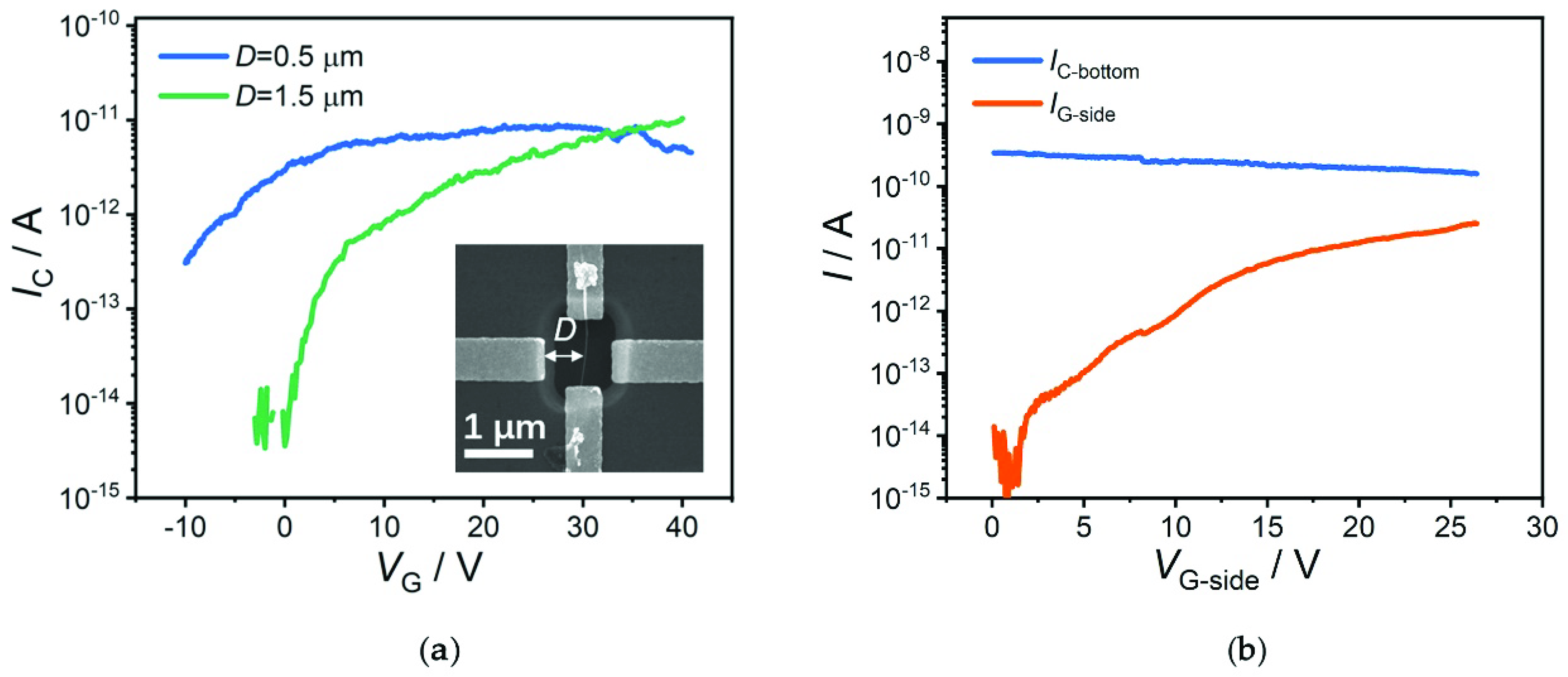
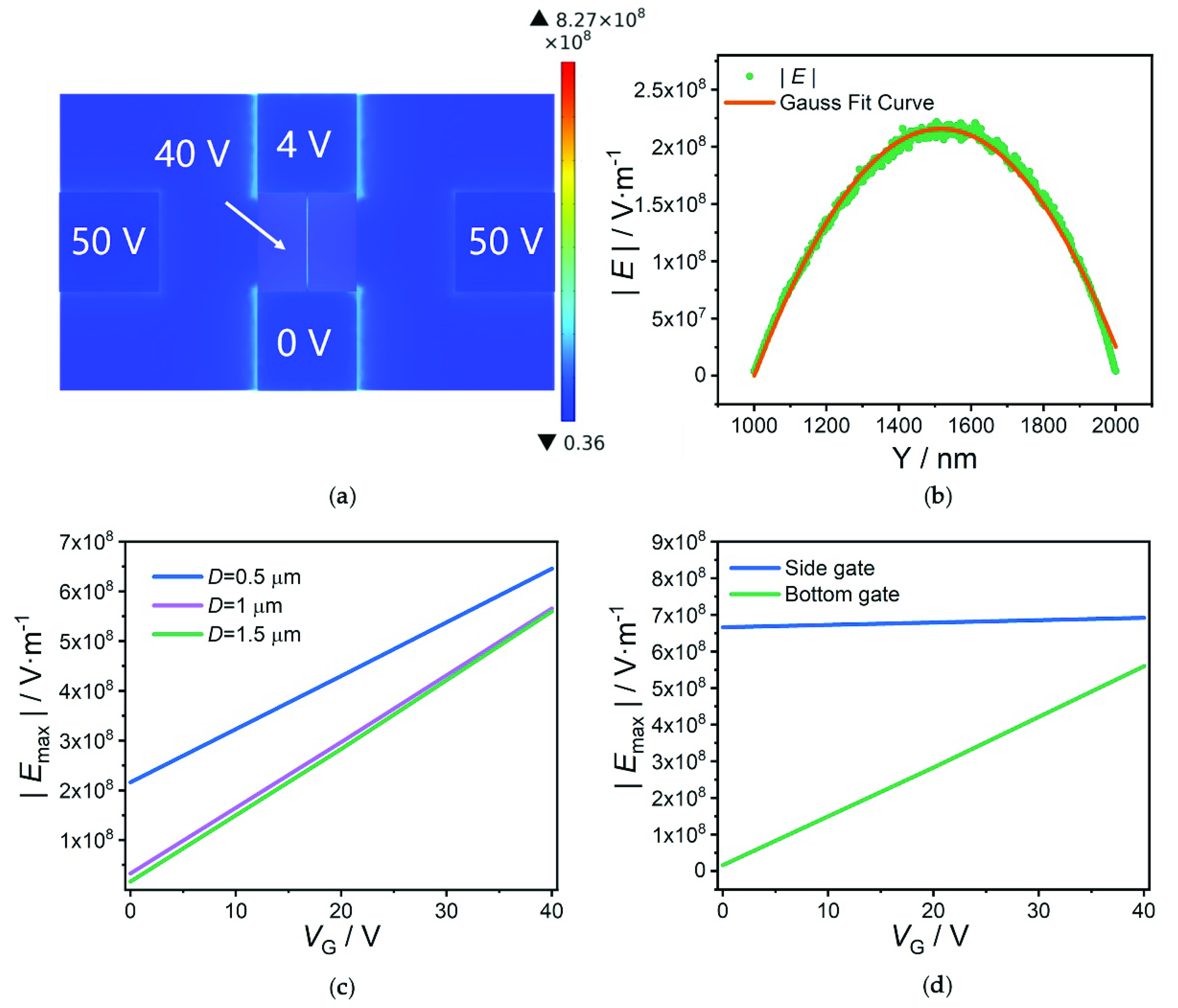
3.3. Gate Controllability and Electric Field Strength Distribution

In order to optimize gate controllability, the dependence of gate controllability on the distance between collector electrodes and electron emitter is explored. Experimental data reveal that the distance (D) has an important influence on the bottom gate controllability. Figure 3a shows the transfer characteristic curves of CVTs with different distances of D = 0.5 μm and D = 1.5 μm, respectively, at VC = 50 V and VDriven = 4.0 V. When the distance is 1.5 μm, the emission current of the CVT increases rapidly with VC in ON state and the ON/OFF current ratio is ~103. When the distance is 0.5 μm, however, the OFF current is so large that the slope of the ICVG curve is smaller than that of the former with a ON/OFF current ratio of ~10. Namely, the device with D of 0.5 μm is hard to be switched OFF. In addition, the emission current decreases slightly with the increase of VG larger than 30 V, which is attributed to gate electrode−capturing electrons. Consequently, the longer the distance of collectors is, the higher performance in bottom gate controllability.
The transfer characteristic is also measured when the bottom Si substrate is set as the collector electrode (designated as bottom collector) and the side electrodes are set as the gate electrode (designated as side gate). Figure 3b shows the curve of bottom−collector current (IC-bottom) versus side-gate voltage (VG-side) curve and that of side-gate current (IG-side) versus side-gate voltage (VG-side) of a CVT. It can be clearly seen that the leakage current collected by side gate (IG-side) increases rapidly with the side-gate voltage. However, the emission current collected by the bottom collector (IC-bottom) maintains stable roughly with the side-gate voltage, indicating a weak gate controllability. The device configuration with the side electrodes as the collector and the bottom electrode as the gate therefore show much better gate controllability than the device configuration with the side electrodes as the gate and the bottom electrode as the collector.
To get further insights into the gate controllability of the devices, electric field in a CVT is calculated by COMSOL. The simulated CVT uses the same parameters as those of the CVT in experiments, including the thickness (90 nm) of metal electrodes, the thickness (300 nm) of SiO2 layer, and the diameter (10 nm) and length (1 μm) of a CNT. To simulate the devices with different distance between the collector electrodes and CNT emitter, we calculated the electric field in the devices with D = 0.5 μm, 1 μm, and 1.5 μm, respectively. Figure 4a shows the distribution of electric field strength of a simulated device with D = 1.5 μm when VG is fixed at 40 V. The distribution of electric field strength along the axis of a CNT emitter is shown in Figure 4b, where the strength of electric field at each axial position is obtained by averaging electric field strength along the circumference of the CNT. The distribution of electric field strength along the CNT axis can be well fitted by a curve of Gauss function. The maximum value of the fitting curve is regarded as the maximum electric field strength (| E m a x |) in the CNT surface.
Figure 4c shows the dependence of | E m a x | on VG for the devices with different D. It can be seen that | E m a x | increases from 1.63 × 10⁷ V·m−1 to 5.60 × 10⁸ V·m−1 by more than 30 times with the increase of VG from 0 V to 40 V when D is 1.5 μm. In contrast, | E m a x | only increases by 2.99 and 17.26 times with the same increase of VG from 0 V to 40 V corresponding to a D of 0.5 μm and 1.0 μm. The CVT with D of 1.5 μm therefore has a stronger gate controllability of | E m a x | by VG than that of other CVTs with shorter D, which is in good agreement with the experimental results in Figure 3a. The poorer gate-to-emitter controllability for shorter collector-to-emitter distance can well be understood, by considering the fact that the electric field at the surface of CNT emitter is mainly governed by the collector but not the gate in the case of short collector-to-emitter distance.
We also calculate | E m a x |−VG curves for different device configurations (the device with the side gate and bottom collector, and the device with the bottom gate and side collector). It can be seen from Figure 4d that, when the distance between CNT and side electrode is 1.5 μm and the distance between CNT and bottom electrode is 300 nm, the device with the side gate and bottom collector shows much less controllability of | E m a x | by VG than the device with the bottom gate and side collector, in agreement with the experimental results in Figure 3b. The stronger gate controllability for device with the bottom gate is attributed to the dominance of electric field at CNT surface by the bottom electrode that is closer to the CNT emitter than the side electrodes.
Considering a gate voltage of 10 V for switching on a CVT, as shown in Figure 2c, an electric field with the maximum magnitude of as small as ~1 × 10⁸ V·m−1 is needed to switch on a CVT according to Figure 4c. This is about one order of magnitude smaller than that needed for the vacuum transistors based on field emission, which requires a typical local threshold electric field of more than 1 × 10⁹ V·m−1. Compared with field emission that is quite sensitive to the microstructures of the emitter, Field-Assisted thermionic emission shows much less sensitivity to the microstructures of the emitter due to the much smaller threshold electric field [18]. Moreover, according to our previous works, the temperature of CNT emitter in a CVT can reach up to more than 2000 K [22]. The absorption of ambient molecules, which is thought to be the main reason for the instability of field emission, can be effectively prevented in such a hot electron emitter. The higher the temperature, the shorter the desorption time of the residual gas molecules. Our CVTs based on Field-Assisted thermionic emission are therefore expected to show better stability and uniformity than the vacuum transistors based on field emission.

4. Conclusions

In conclusion, we report a new structure of vacuum transistor based on Field-Assisted thermionic emission with individual CNTs as the filaments, fabricated by microfabrication technologies. The emission current can be controlled by tuning the bias voltage applied to the heavily doped Si substrate with an ON/OFF current ratio up to 104 and a subthreshold slope of ~4 V·dec−1. Furthermore, we explore the influence of distance between collector electrodes and electron emitter on gate controllability and find that the longer the distance is, the stronger the gate controllability to electron emission is. Benefiting from Field-Assisted thermionic emission, the emission current of CVTs is much less sensitive to the microstructures of emitter and absorption of ambient molecules. The CVTs are therefore expected to show better stability and uniformity than the vacuum transistors based on field emission.

Author Contributions

Conceptualization, X.W. and Y.H.; methodology, Y.H. and Z.L.; software, Y.H. and S.M.; validation, Y.H.; formal analysis, Y.H., Z.L. and F.Z.; investigation, X.W. and Y.H.; resources, X.W.; data curation, Y.H.; writing—original draft preparation, Y.H.; writing—review and editing, X.W., Z.L. and Y.H.; funding acquisition, X.W. All authors have read and agreed to the published version of the manuscript.

Funding

This work was funded by the National Key Research and Development Program of China (Grant No. 2017YFA0205003, 2019YFA0210201) and the National Natural Science Foundation of China (Grant No. 62022007, 11874068, 11890671).

Data Availability Statement

The data presented in this study are available on request from the corresponding author. The data are not publicly available due to privacy.

Conflicts of Interest

The authors declare no conflict of interest.

References

  1. Koomey, J.; Berard, S.; Sanchez, M.; Wong, H. Implications of Historical Trends in the Electrical Efficiency of Computing. IEEE Ann. Hist. Comput. 2011, 33, 46–54. [Google Scholar] [CrossRef]
  2. Kim, H.K. Vacuum transistors for space travel. Nat. Electron. 2019, 2, 374–375. [Google Scholar] [CrossRef]
  3. Brinkman, W.F.; Haggan, D.E.; Troutman, W.W. A history of the invention of the transistor and where it will lead us. IEEE J. Solid-State Circuits 1997, 32, 1858–1865. [Google Scholar] [CrossRef] [Green Version]
  4. Barbour, E. The cool sound of tubes [vacuum tube musical applications]. IEEE Spectr. 1998, 35, 24–35. [Google Scholar] [CrossRef]
  5. Stoner, B.R.; Glass, J.T. Nothing is like a vacuum. Nat. Nanotechnol. 2012, 7, 485–487. [Google Scholar] [CrossRef]
  6. Liu, W.; Liu, Y.; Jia, Q.; Sun, B.; Chen, J. Terahertz laser diode using field emitter arrays. Phys. Rev. B 2021, 103, 035109. [Google Scholar] [CrossRef]
  7. Han, J.-W.; Seol, M.-L.; Moon, D.-I.; Hunter, G.; Meyyappan, M. Nanoscale vacuum channel transistors fabricated on silicon carbide wafers. Nat. Electron. 2019, 2, 405–411. [Google Scholar] [CrossRef]
  8. Nirantar, S.; Ahmed, T.; Ren, G.; Gutruf, P.; Xu, C.; Bhaskaran, M.; Walia, S.; Sriram, S. Metal–Air Transistors: Semiconductor-Free Field-Emission Air-Channel Nanoelectronics. Nano Lett. 2018, 18, 7478–7484. [Google Scholar] [CrossRef]
  9. Jennings, S.G. The mean free path in air. J. Aerosol Sci. 1988, 19, 159–166. [Google Scholar] [CrossRef]
  10. Han, J.-W.; Moon, D.-I.; Meyyappan, M. Nanoscale Vacuum Channel Transistor. Nano Lett. 2017, 17, 2146–2151. [Google Scholar] [CrossRef]
  11. Bower, C.; Zhu, W.; Shalom, D.; Lopez, D.; Chen, L.H.; Gammel, P.L.; Jin, S. On-chip vacuum microtriode using carbon nanotube field emitters. Appl. Phys. Lett. 2002, 80, 3820–3822. [Google Scholar] [CrossRef]
  12. Bhattacharya, R.; Han, J.W.; Browning, J.; Meyyappan, M. Complementary Vacuum Field Emission Transistor. IEEE Trans. Electron Devices 2021, 68, 5244–5249. [Google Scholar] [CrossRef]
  13. Han, J.-W.; Seol, M.-L.; Kim, J.; Meyyappan, M. Nanoscale Complementary Vacuum Field Emission Transistor. ACS Appl. Nano Mater. 2020, 3, 11481–11488. [Google Scholar] [CrossRef]
  14. Wang, X.; Xue, T.; Shen, Z.; Long, M.; Wu, S. Analysis of the electron emission characteristics and working mechanism of a planar bottom gate vacuum field emission triode with a nanoscale channel. Nanoscale 2021, 13, 14363–14370. [Google Scholar] [CrossRef]
  15. Chang, W.T.; Pao, P.H. Field Electrons Intercepted by Coplanar Gates in Nanoscale Air Channel. IEEE Trans. Electron Devices 2019, 66, 3961–3966. [Google Scholar] [CrossRef]
  16. Khoshkbijari, F.K.; Sharifi, M.J. Finger Gate Vacuum Channel Field Emission Transistors: Performance and Sensitivity Analysis. IEEE Trans. Electron Devices 2021, 68, 5250–5256. [Google Scholar] [CrossRef]
  17. Fan, L.; Bi, J.; Xi, K.; Zhao, B.; Yang, X.; Xu, Y. Sub-10-nm Air Channel Field Emission Device with Ultra-Low Operating Voltage. IEEE Electron Device Lett. 2021, 42, 1390–1393. [Google Scholar] [CrossRef]
  18. Terrones, M.; Terrones, H.; de Jonge, N.; Bonard, J.M. Carbon nanotube electron sources and applications. Philos. Trans. R. Soc. Lond. Ser. A Math. Phys. Eng. Sci. 2004, 362, 2239–2266. [Google Scholar]
  19. Wu, G.; Wei, X.; Zhang, Z.; Chen, Q.; Peng, L. A Graphene-Based Vacuum Transistor with a High ON/OFF Current Ratio. Adv. Funct. Mater. 2015, 25, 5972–5978. [Google Scholar] [CrossRef]
  20. Wei, X.; Golberg, D.; Chen, Q.; Bando, Y.; Peng, L. Phonon-Assisted Electron Emission from Individual Carbon Nanotubes. Nano Lett. 2011, 11, 734–739. [Google Scholar] [CrossRef]
  21. Wei, X.; Wang, S.; Chen, Q.; Peng, L. Breakdown of Richardson’s Law in Electron Emission from Individual Self-Joule-Heated Carbon Nanotubes. Sci. Rep. 2014, 4, 5102. [Google Scholar] [CrossRef] [PubMed] [Green Version]
  22. Wang, Y.; Wu, G.; Xiang, L.; Xiao, M.; Li, Z.; Gao, S.; Chen, Q.; Wei, X. Single-walled carbon nanotube thermionic electron emitters with dense, efficient and reproducible electron emission. Nanoscale 2017, 9, 17814–17820. [Google Scholar] [CrossRef] [PubMed]
  23. Lazzeri, M.; Piscanec, S.; Mauri, F.; Ferrari, A.C.; Robertson, J. Electron Transport and Hot Phonons in Carbon Nanotubes. Phys. Rev. Lett. 2005, 95, 236802. [Google Scholar] [CrossRef] [PubMed]
  24. Pop, E.; Mann, D.; Cao, J.; Wang, Q.; Goodson, K.; Dai, H. Negative Differential Conductance and Hot Phonons in Suspended Nanotube Molecular Wires. Phys. Rev. Lett. 2005, 95, 155505. [Google Scholar] [CrossRef] [Green Version]
  25. Herring, C.; Nichols, M.H. Thermionic Emission. Rev. Mod. Phys. 1949, 21, 185–270. [Google Scholar] [CrossRef]
  26. Jin, F.; Liu, Y.; Day, C.M.; Little, S.A. Enhanced electron emission from functionalized carbon nanotubes with a barium strontium oxide coating produced by magnetron sputtering. Carbon 2007, 45, 587–593. [Google Scholar] [CrossRef]
Figure 1. (a) A schematic illustration and working principles of a CNT-based vacuum transistor; (b) an SEM image of a global CVT; (c) an SEM image of the framed area in image (b).
Electronics 11 00399 g001
Figure 2. The performances of CVTs with distance between collector electrode and CNT emitter of 1.5 μm measured at room temperature and ~1 × 10⁻² Pa. (a) The emission performance of a CNT emitter is measured repeatedly for five times when VC is fixed at 50 V; (b) output characteristic (ICVDriven curves) and (c) transfer characteristic (ICVG curves) of a CVT at various gate voltages and driven voltages. The dashed lines and solid lines in (b) are in exponential and linear scale, respectively; (d) transfer characteristic of the same device in (c) when VC is 50 V and VDriven is 4.2 V, which indicates an ON/OFF current ratio up to 104. The black line shows the relationship between IG and VG.
Electronics 11 00399 g002
Figure 3. (a) Transfer characteristic of two CVTs with different distances between collector electrodes and CNT emitter: 0.5 μm and 1.5 μm. Inset: a scanning electron microscope image of a CVT with D = 0.5 μm; (b) simultaneously measured ICVG curve and IGVG curve of a CVT with the heavily doped Si substrate as the collector and side electrodes as the side-gate.
Electronics 11 00399 g003
Figure 4. Electric field distribution simulations of a CNT-based vacuum transistor. (a) Electric field strength distribution in a simulation model with VDriven = 4.0 V, VC = 50 V, VG = 40 V; (b) the distribution of electric field strength around the CNT surface along the axis of the carbon nanotube when D is 0.5 μm, VDriven = 4.0 V, VC = 50 V, VG = 0 V; (c) | E m a x |−VG curves for the devices with the side electrodes as the collector and D of 0.5 μm, 1 μm, 1.5 μm; (d) | E m a x |−VG curves for the devices (D = 1.5 μm) with the bottom gate and side gate, respectively.
Electronics 11 00399 g004
Publisher’s Note: MDPI stays neutral with regard to jurisdictional claims in published maps and institutional affiliations.

