
Effects of Random Switching Schemes on the EMI Levels of Conventional and Interleaved Buck Converters for Mobile Devices

 ,
, 
 ,
,
Abstract
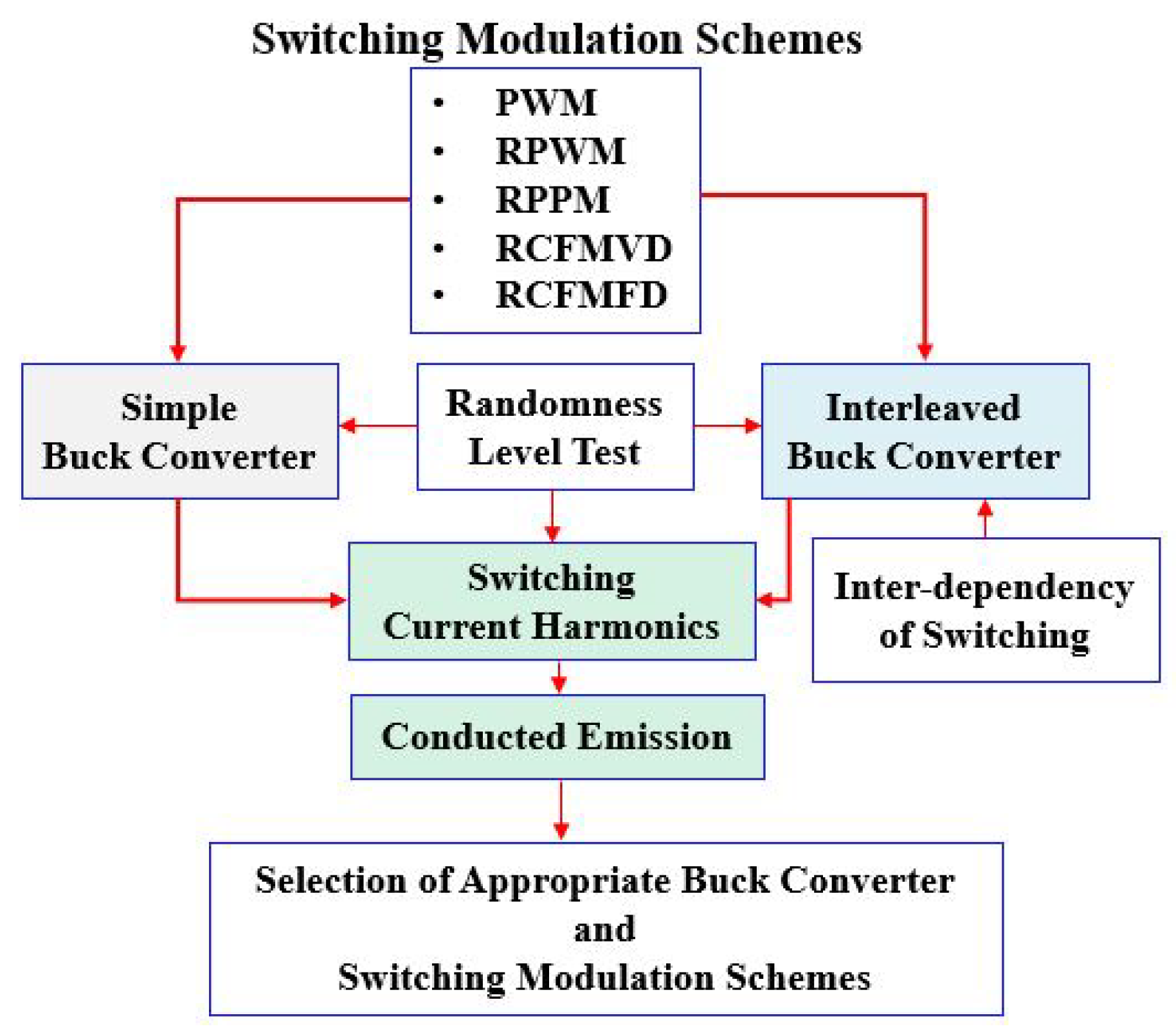
:1. Introduction
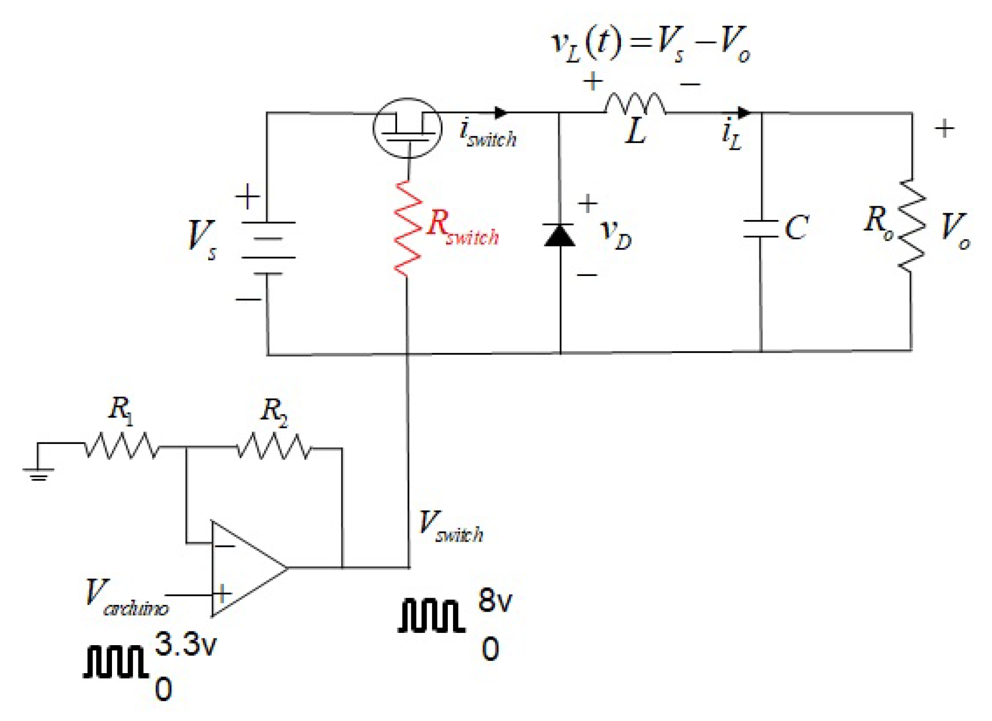
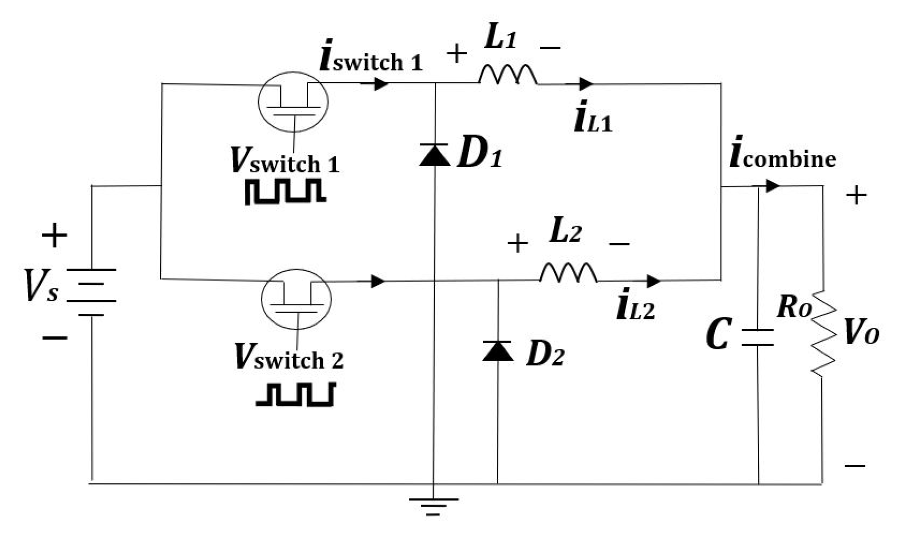
2. Buck Converter Circuits
2.1. Simple Buck Converter
2.2. Interleaved Buck Converter
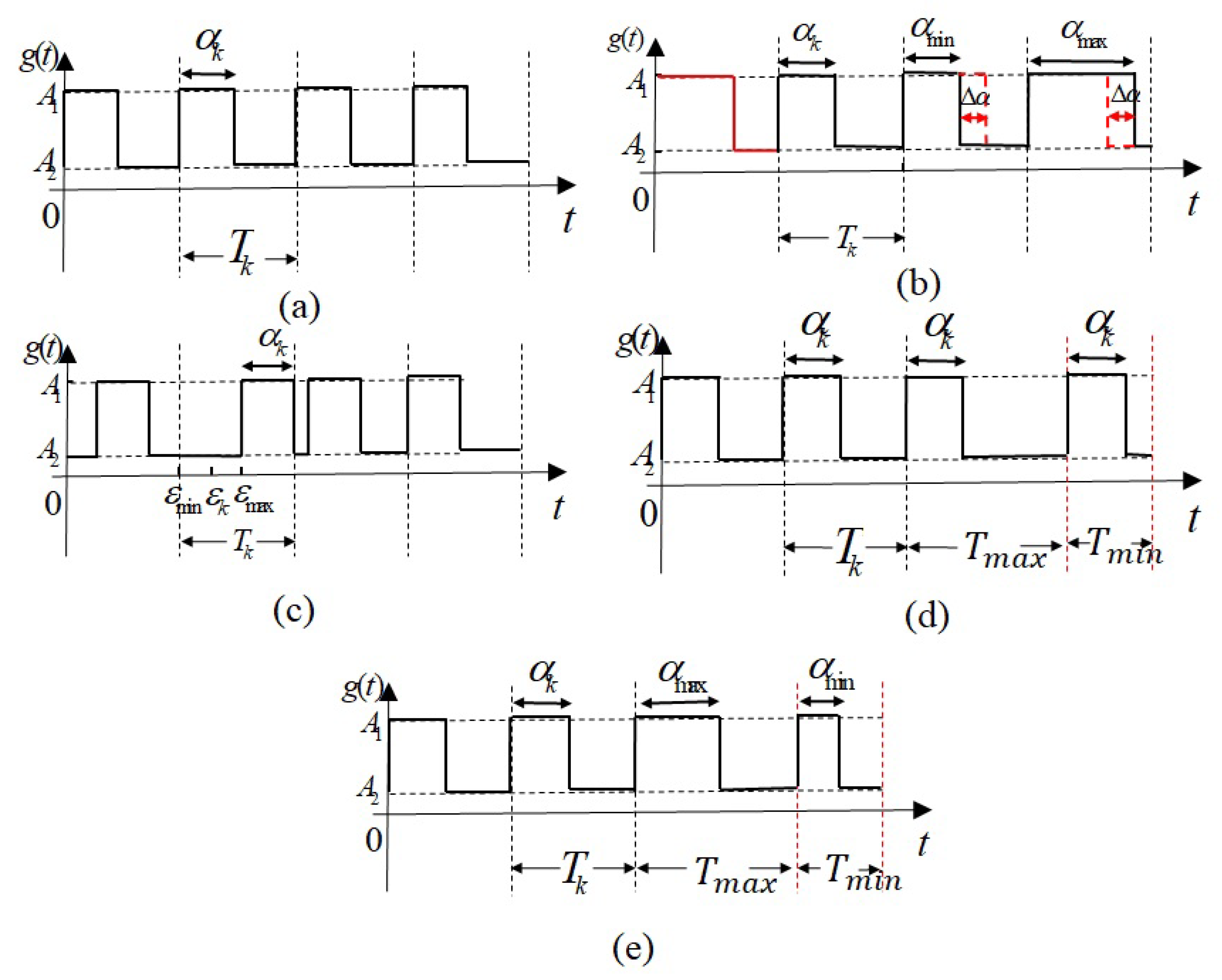
3. Random Modulation Switching Schemes
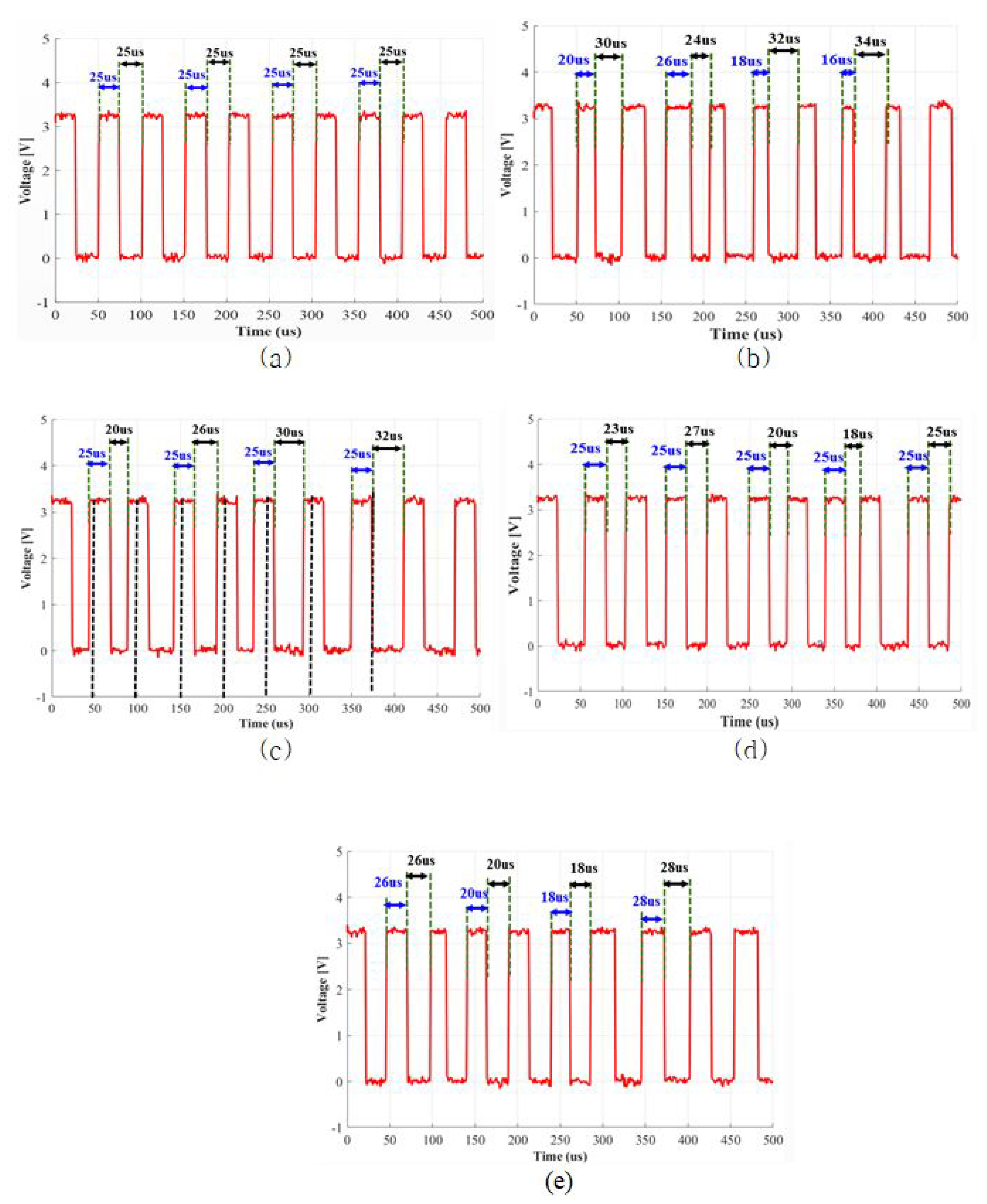
3.1. Switching Modulation Schemes for Simple Buck Converter
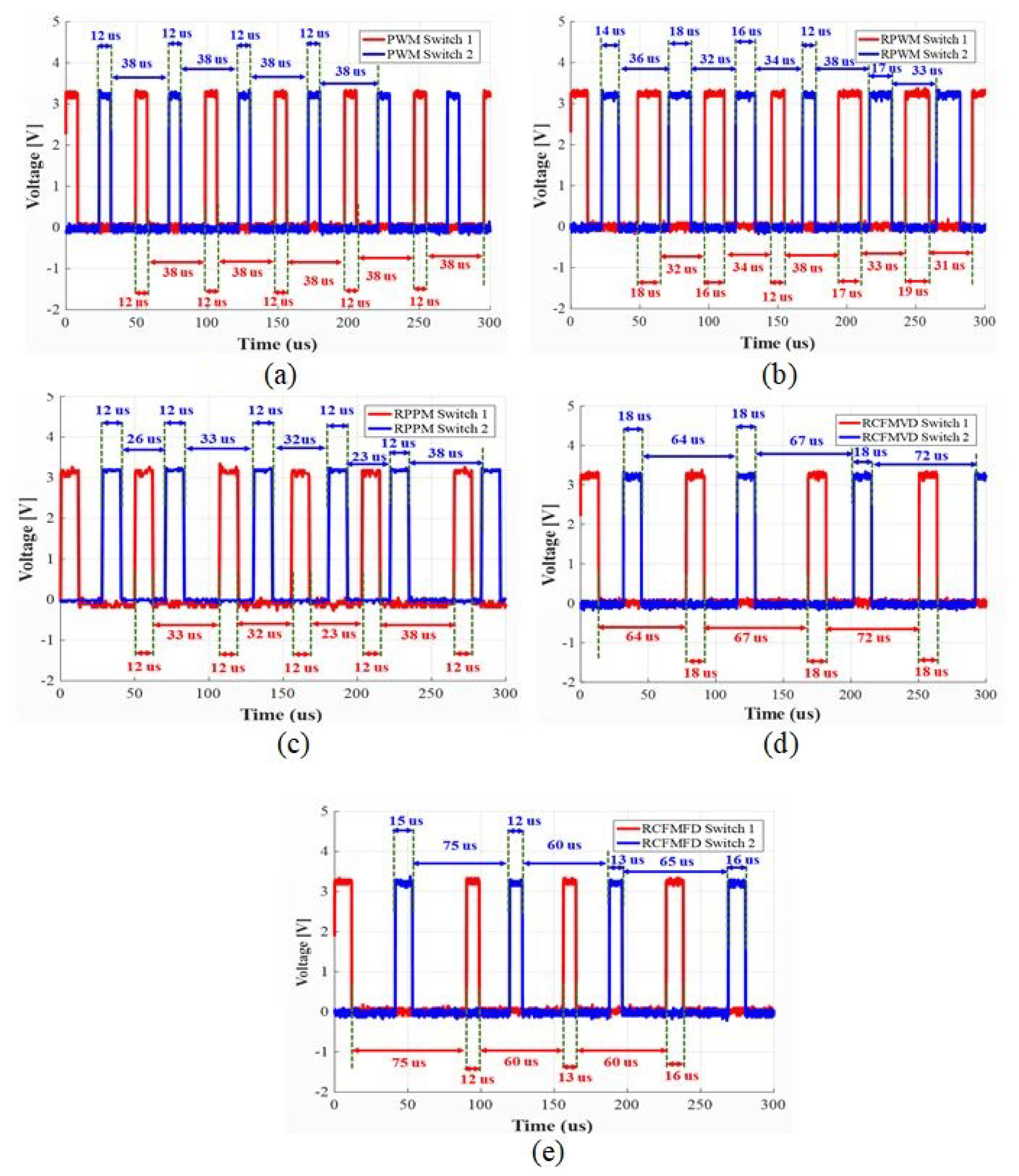
3.2. Switching Modulation Schemes for an Interleaved Buck Converter
4. Switching Current Harmonics Analysis
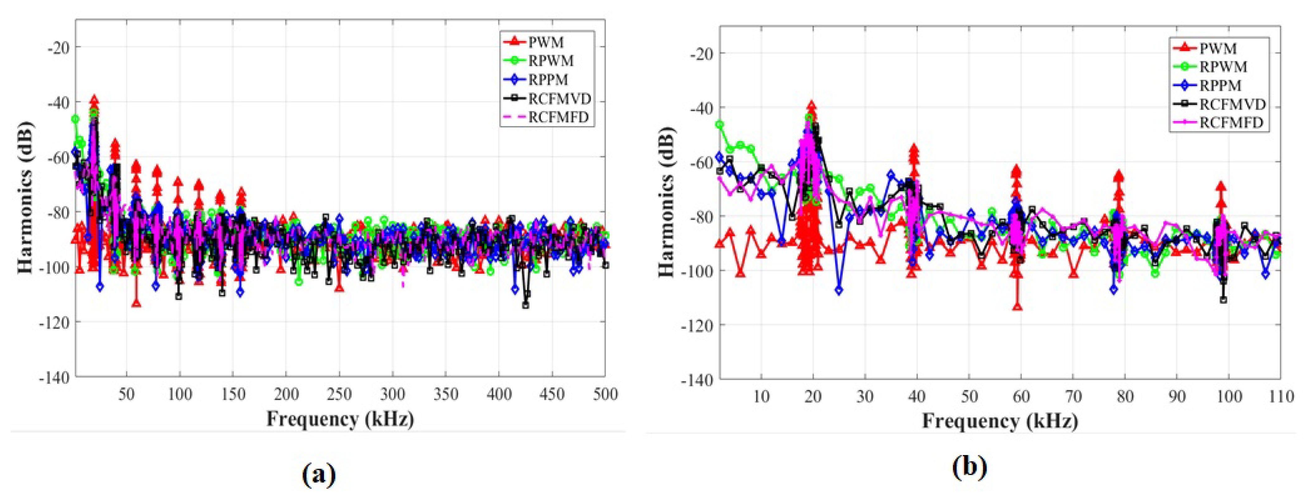
4.1. Switching Current Harmonic Results for Simple Buck Converter
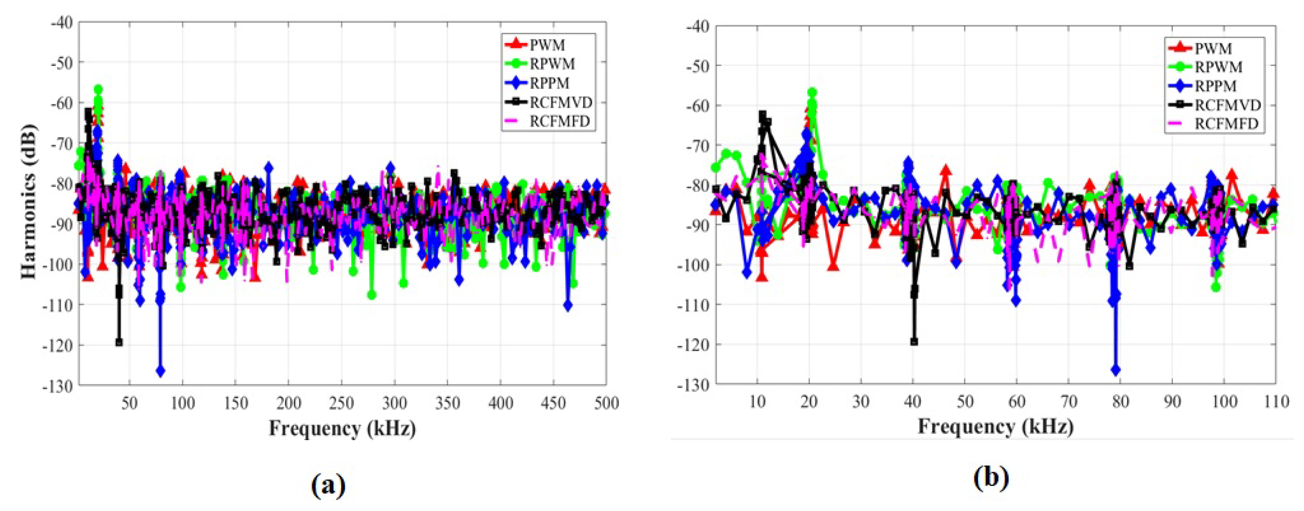
4.2. Switching Current Harmonic Results for an Interleaved Buck Converter
5. Conducted Emission (CE) Analysis
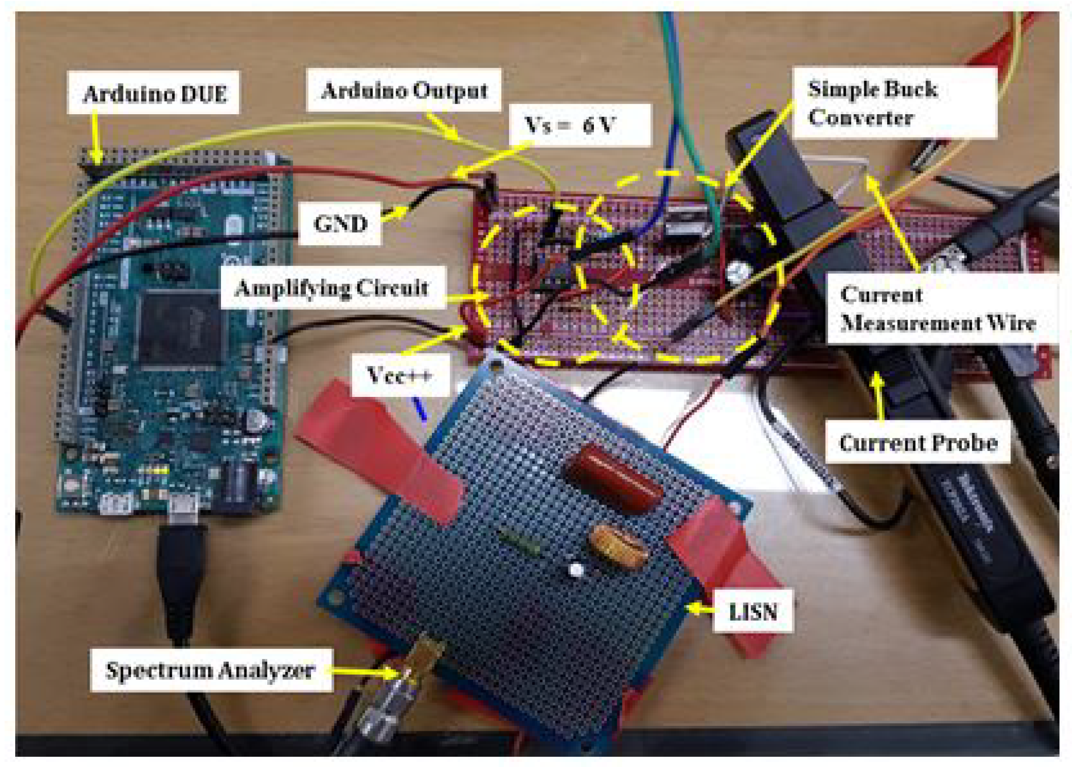
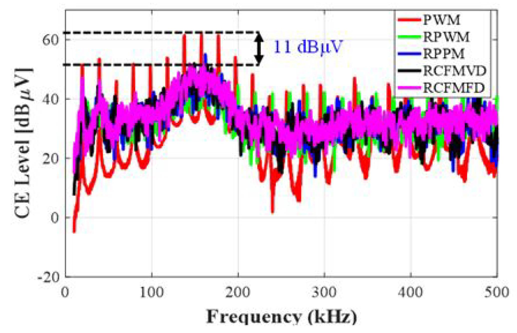
5.1. Conducted Emission Analysis for Simple Buck Converter
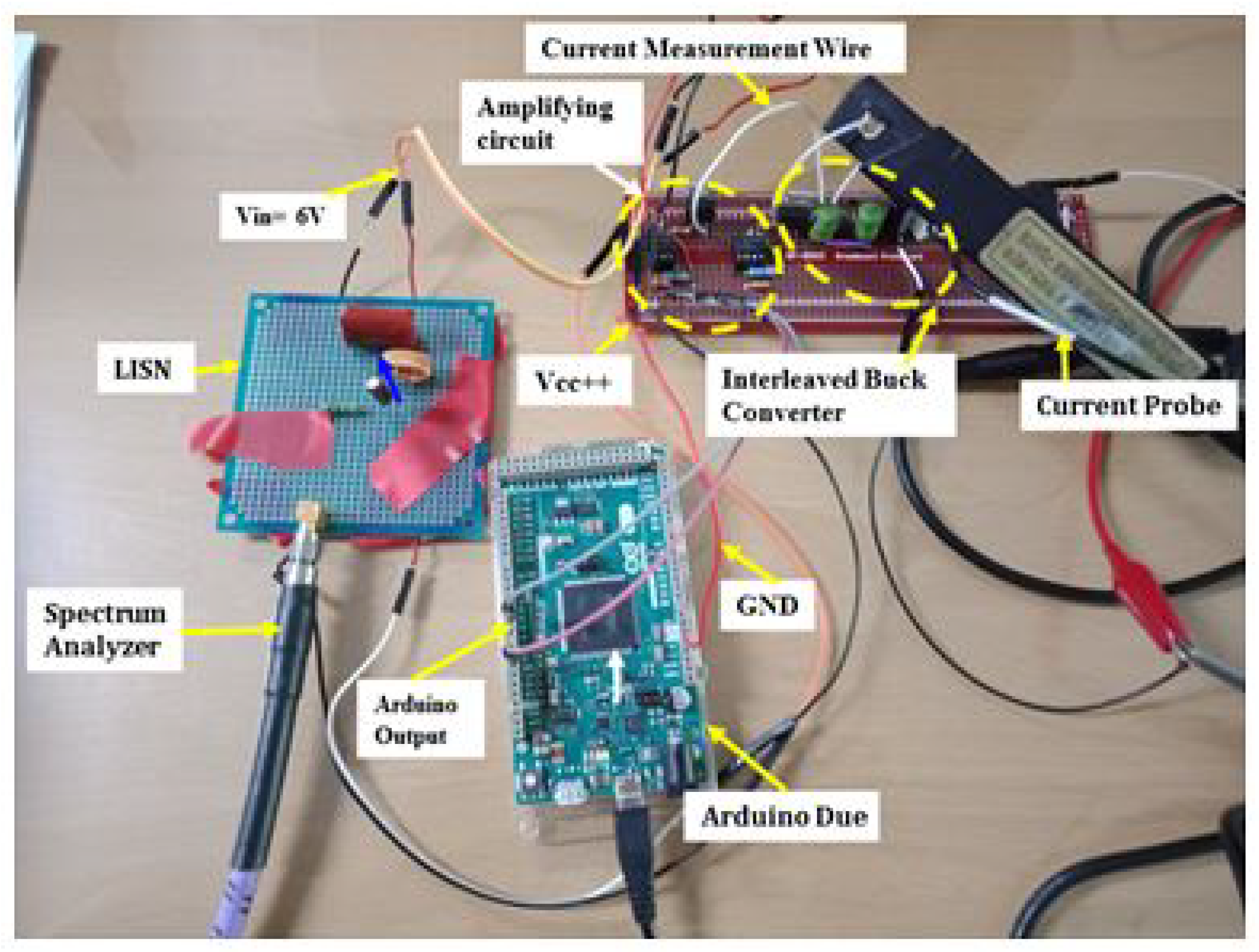
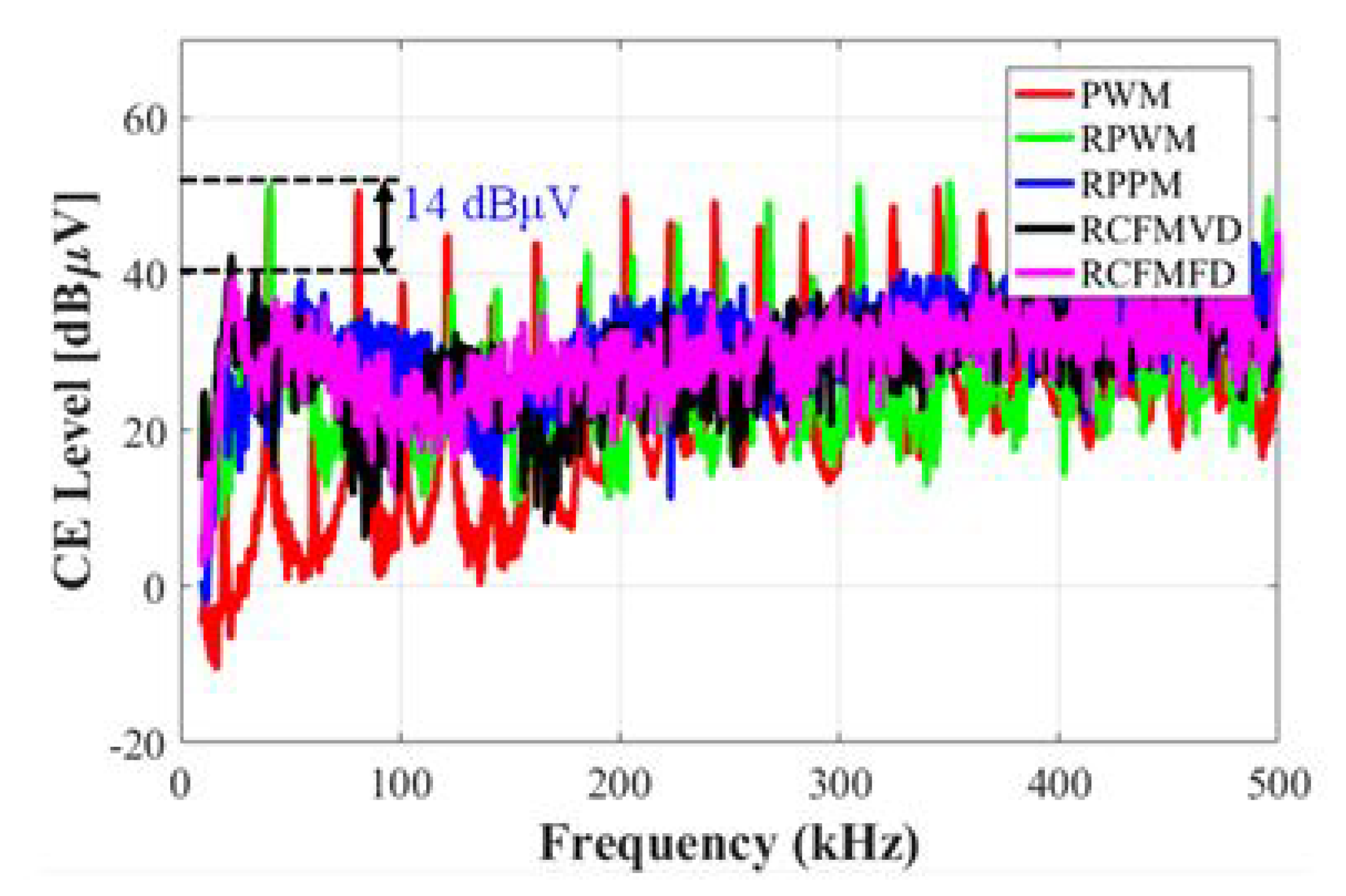
5.2. Conducted Emission Analysis for an Interleaved Buck Converter
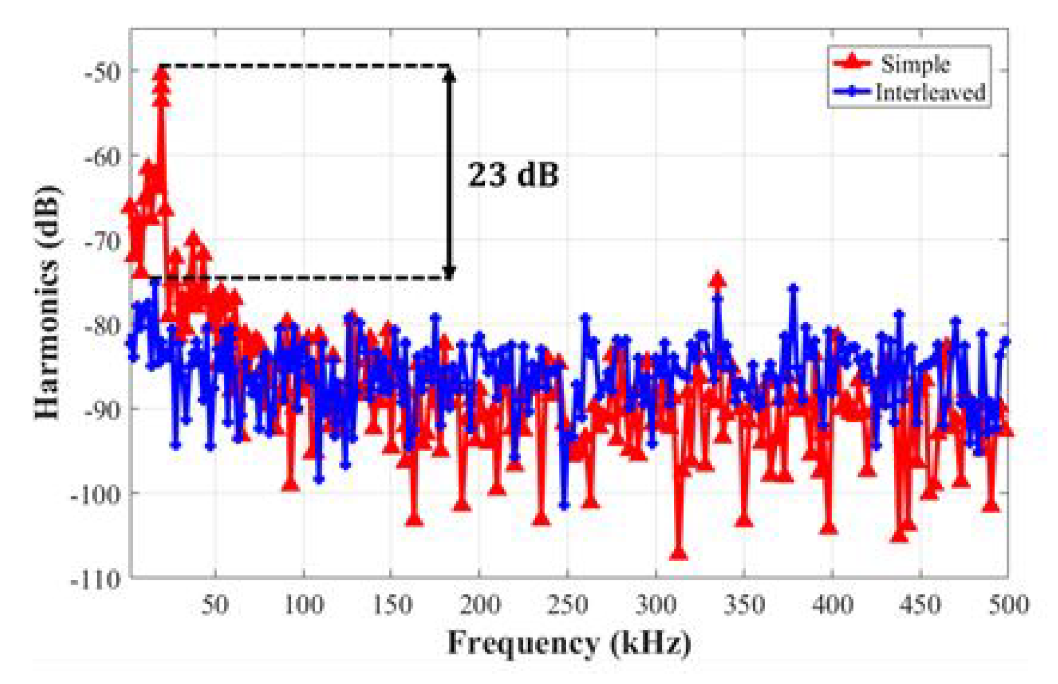
6. Comparison
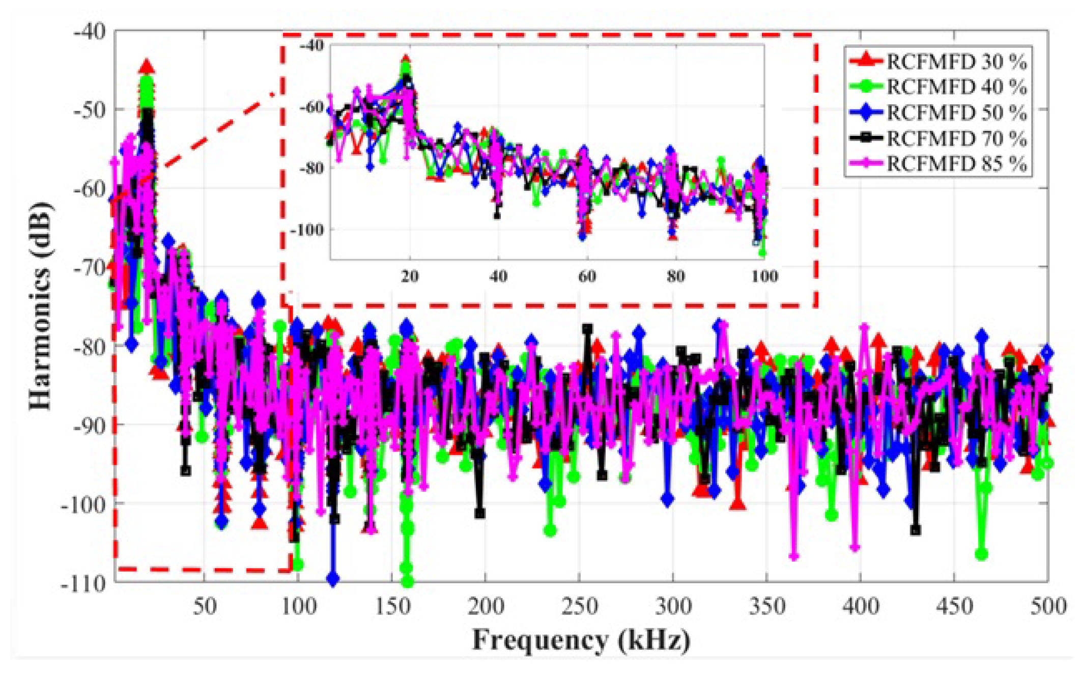
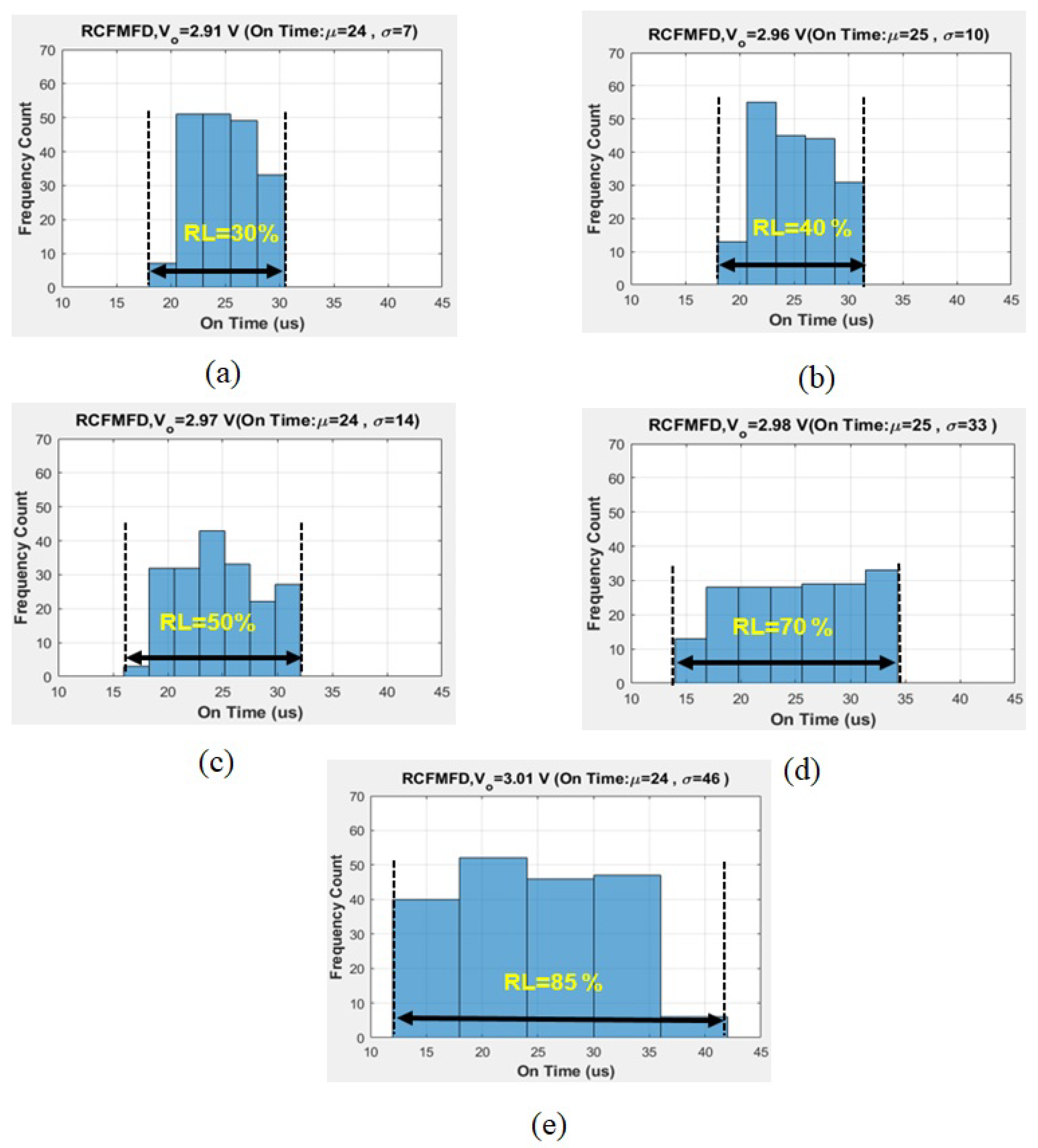
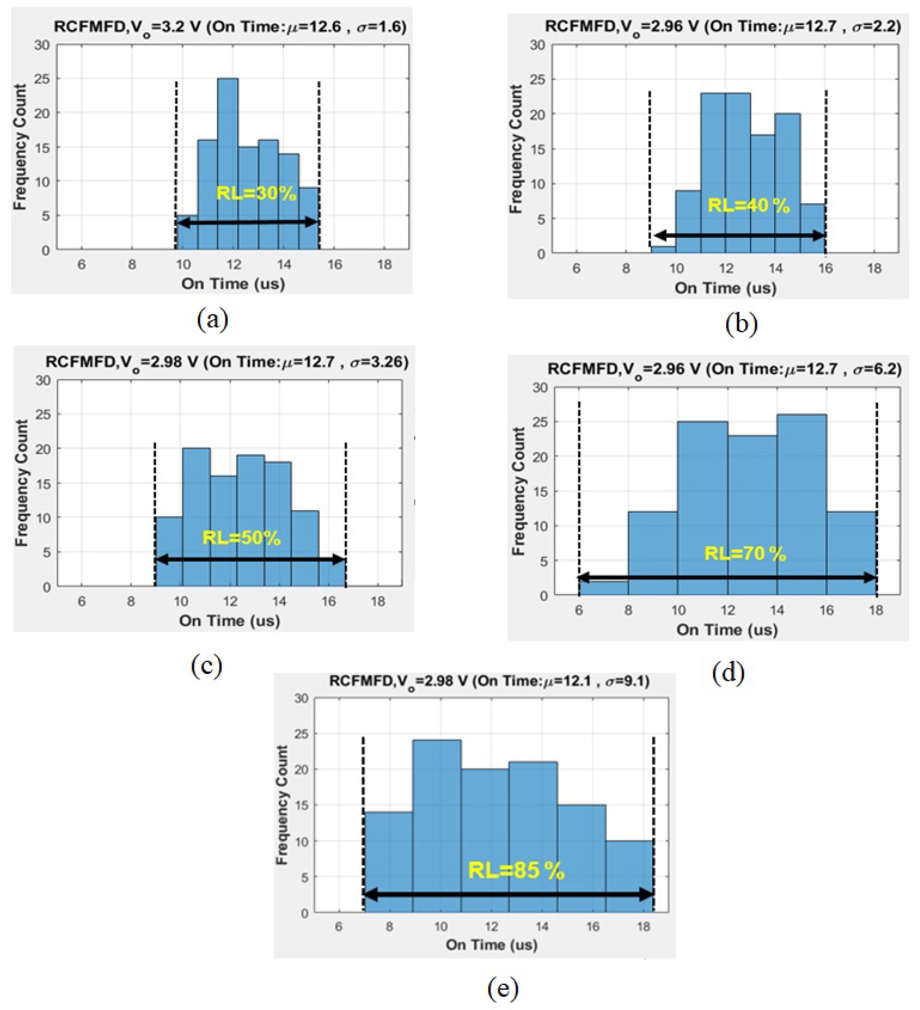
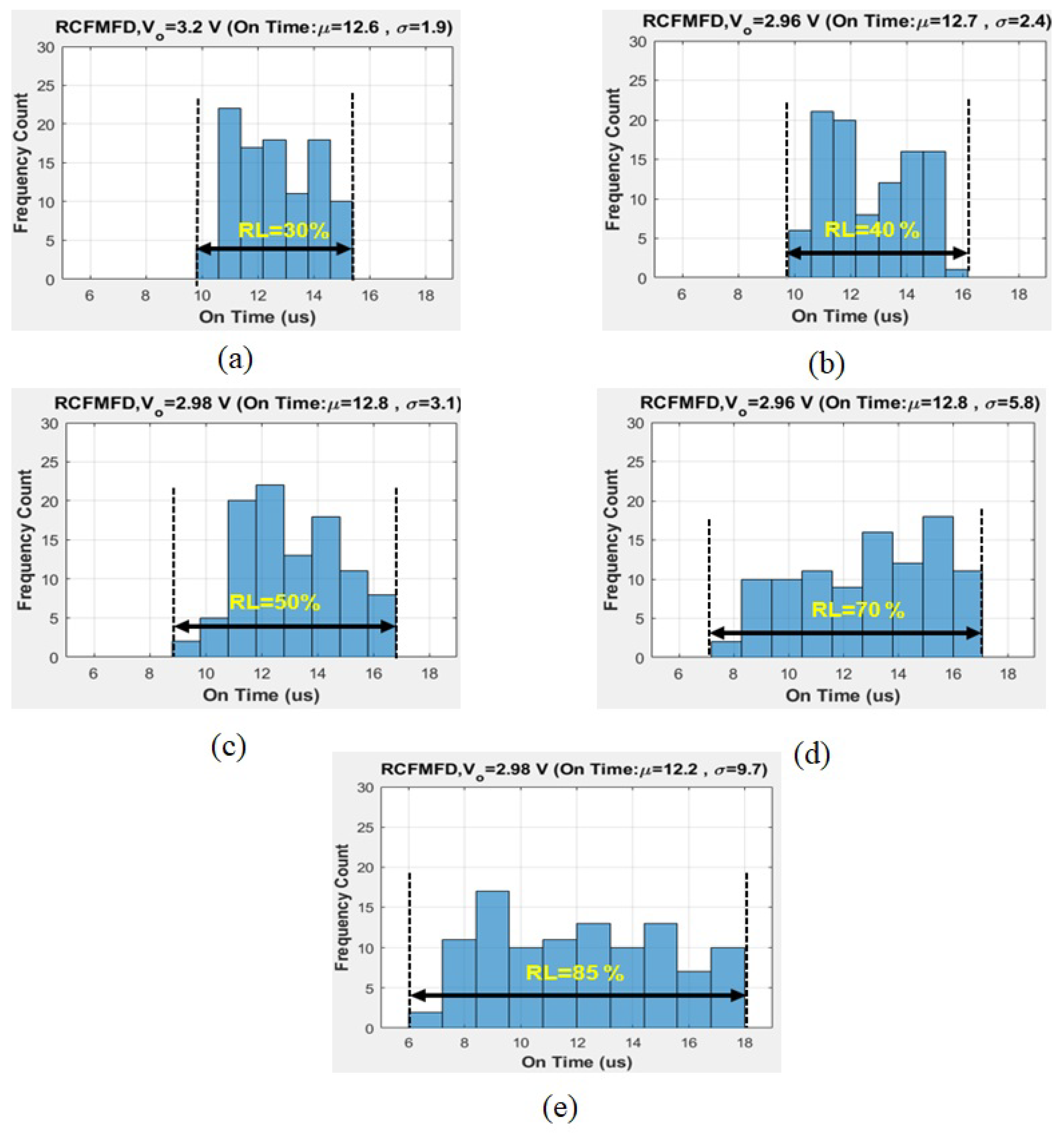
7. Impact of Randomness Level (RL)
7.1. Randomness Level Analysis for Simple Buck Converter
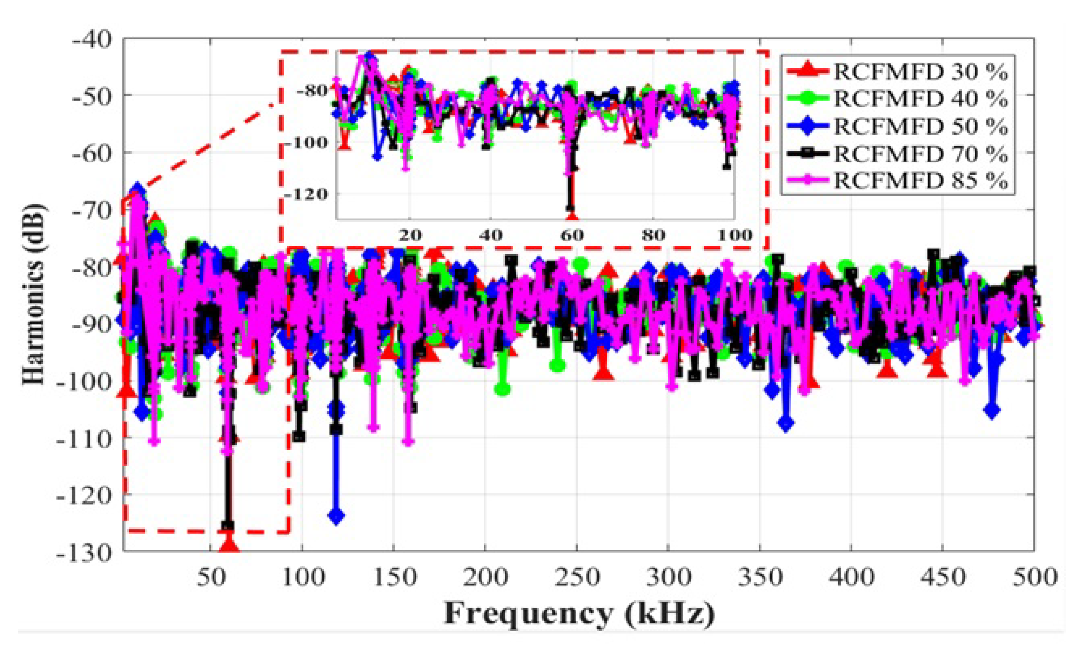
7.2. Randomness Level Analysis for an Interleaved Buck Converter
8. Interleaved Switching Dependency
9. Conclusions
Author Contributions
Funding
Conflicts of Interest
References
- Tse, K.; Chung, H.H.; Hui, S.; So, H. A comparative investigation on the use of random modulation schemes for DC/DC converters. IEEE Trans. Ind. Electron. 2000, 47, 253–263. [Google Scholar] [CrossRef] [Green Version]
- Yang, Y.; Li, D.; Wang, D. Dynamic Analysis of the Switched-Inductor Buck-Boost Converter Based on the Memristor. Electronics 2021, 10, 452. [Google Scholar] [CrossRef]
- Surya, S.; Srinivasan, M.K.; Williamson, S. Modeling of Average Current in Non-Ideal Buck and Synchronous Buck Converters for Low Power Application. Electronics 2021, 10, 2672. [Google Scholar] [CrossRef]
- Laour, M.; Tahmi, R.; Vollaire, C. Modeling and Analysis of Conducted and Radiated Emissions Due to Common Mode Current of a Buck Converter. IEEE Trans. Electromagn. Compat. 2017, 59, 1260–1267. [Google Scholar] [CrossRef]
- Guilbert, D.; Sorbera, D.; Vitale, G. A stacked interleaved DC-DC buck converter for proton exchange membrane electrolyzer applications: Design and experimental validation. Int. J. Hydrogen Energy 2020, 45, 64–79. [Google Scholar] [CrossRef]
- Sayed, W.E.; Lezynski, P.; Smolenski, R.; Moonen, N.; Crovetti, P.; Thomas, D.W.P. The Effect of EMI Generated from Spread-Spectrum-Modulated SiC-Based Buck Converter on the G3-PLC Channel. Electronics 2021, 10, 1416. [Google Scholar] [CrossRef]
- Stone, D.; Chambers, B. The Effect of Carrier Frequency Modulation of PWM Waveforms on Conducted EMC Problems in Switched Mode Power Supplies. EPE J. 1996, 5, 32–37. [Google Scholar] [CrossRef]
- Lin, F.; Chen, D. Reduction of power supply EMI emission by switching frequency modulation. IEEE Trans. Power Electron. 1994, 9, 132–137. [Google Scholar] [CrossRef]
- Lee, I.O.; Cho, S.Y.; Moon, G.W. Interleaved Buck Converter Having Low Switching Losses and Improved Step-Down Conversion Ratio. IEEE Trans. Power Electron. 2012, 27, 3664–3675. [Google Scholar] [CrossRef]
- Aulagnier, G.; Abouda, K.; Rolland, E.; Cousineau, M.; Meynard, T. Benefits of multiphase Buck converters in reducing EME (Electromagnetic Emissions) Analysis and application to on-chip converters for automotive applications. In Proceedings of the 2015 IEEE International Symposium on Electromagnetic Compatibility (EMC), Dresden, Germany, 16–22 August 2015; pp. 102–107. [Google Scholar] [CrossRef]
- Mon, J.; Gago, J.; Díez, D.; Balcells, J.; Fernandez-Garcia, R.; Gil, I.; Bogónez-Franco, P. EMI reduction by means of switching frequency modulation with variable delay in power supplies. Int. J. Electron. 2012, 99, 103–112. [Google Scholar] [CrossRef]
- Ferrazza, F.; Cacciotto, F.; de Simone, S.; Rapisarda, S.; Adragna, C. Implementation of artificial frequency modulation in boundary mode power converters for EMI reduction. In Proceedings of the 2020 AEIT International Annual Conference (AEIT), Catania, Italy, 23–25 September 2020; pp. 1–6. [Google Scholar] [CrossRef]
- Mukherjee, R.; Patra, A.; Banerjee, S. Impact of a Frequency Modulated Pulsewidth Modulation (PWM) Switching Converter on the Input Power System Quality. IEEE Trans. Power Electron. 2010, 25, 1450–1459. [Google Scholar] [CrossRef]
- Ballo, A.; Grasso, A.D.; Palumbo, G. A simple and effective design strategy to increase power conversion efficiency of linear charge pumps. Int. J. Circuit Theory Appl. 2020, 48, 157–161. [Google Scholar] [CrossRef]
- Ballo, A.; Grasso, A.D.; Palumbo, G.; Tanzawa, T. Charge Pumps for Ultra-Low-Power Applications: Analysis, Design, and New Solutions. IEEE Trans. Circuits Syst. II Express Briefs 2021, 68, 2895–2901. [Google Scholar] [CrossRef]
- Mohammed, S.A.; Dogan, H.; Ozgun, M.T. An 85%-efficiency reconfigurable multiphase switched capacitor DC-DC converter utilizing frequency, switch size, and interleaving scaling techniques. Microelectron. J. 2017, 67, 155–161. [Google Scholar] [CrossRef]
- Carbajal-Retana, M.; Hernandez-Gonzalez, L.; Ramirez-Hernandez, J.; Avalos-Ochoa, J.G.; Guevara-Lopez, P.; Loboda, I.; Sotres-Jara, L.A. Interleaved Buck Converter for Inductive Wireless Power Transfer in DC–DC Converters. Electronics 2020, 9, 949. [Google Scholar] [CrossRef]
- Joseph, A.; Francis, J. Design and simulation of two phase interleaved buck converter. Int. J. Adv. Res. Electr. Electron. Instrum. Eng. 2015, 4, 8–15. [Google Scholar]
- Tahavorgar, A.; Quaicoe, J.E. Modeling and prediction of conducted EMI noise in a 2-stage interleaved boost DC/DC converter. In Proceedings of the 2014 16th International Conference on Harmonics and Quality of Power (ICHQP), Bucharest, Romania, 25–28 May 2014; pp. 117–121. [Google Scholar] [CrossRef]
- Lu, W.; Jing, F.; Zhou, L.; Iu, H.H.C.; Fernando, T. Control of sub-harmonic oscillation in peak current mode buck converter with dynamic resonant perturbation. Int. J. Circuit Theory Appl. 2015, 43, 1399–1411. [Google Scholar] [CrossRef]
- Nguyen, V.H.; Huynh, H.A.; Kim, S.; Song, H. Active EMI Reduction Using Chaotic Modulation in a Buck Converter with Relaxed Output LC Filter. Electronics 2018, 7, 254. [Google Scholar] [CrossRef] [Green Version]
- Lin, J.Y.; Hsu, Y.C.; Lin, Y.D. A Low EMI DC-DC Buck Converter with a Triangular Spread-Spectrum Mechanism. Energies 2020, 13, 856. [Google Scholar] [CrossRef] [Green Version]
- Rashid, M.H. Power Electronics: Circuits, Devices, and Applications; Pearson Education: London, UK, 2009. [Google Scholar]
- Yousaf, J.; Amin, M.; Iqbal, S.; Durrani, H. Analysis of Conducted Emission Measurements of DC-DC Converter with Load for Proper Filter Design. Int. J. Microw. Opt. Technol. 2015, 10, 464–470. [Google Scholar]


| Modulatiton | Tk | dk = /Tk | ||
|---|---|---|---|---|
| PWM | constant | constant | zero | constant |
| RPWM | constant | random | zero | random |
| RPPM | constant | constant | random | constant |
| RCFMVD | random | constant | zero | random |
| RCFMFD | random | random | zero | constant |
| Frequency (kHz) | 20 | 40 | 60 | 80 | 100 | |
|---|---|---|---|---|---|---|
| Harmonics | First | Second | Third | Fourth | Fifth | |
| Switching Schemes | PWM | −39 | −55 | −63 | −65 | −69 |
| RPWM | −44 | −69 | −78 | −80 | −81 | |
| RPPM | −49 | −64 | −75 | −79 | −80 | |
| RCFMVD | −47 | −67 | −77 | −78 | −82 | |
| RCFMFD | −46 | −67 | −75 | −80 | −80 | |
| Frequency (kHz) | 20 | 40 | 60 | 80 | 100 | |
|---|---|---|---|---|---|---|
| Harmonics (dB) | First | Second | Third | Fourth | Fifth | |
| Switching Schemes | PWM | −61 | −70 | −74 | −79 | −79 |
| RPWM | −56 | −69 | −78 | −79 | −81 | |
| RPPM | −67 | −74 | −79 | −80 | −80 | |
| RCFMVD | −75 | −76 | −78 | −79 | −81 | |
| RCFMFD | −78 | −79 | −80 | −81 | −80 | |
| Schemes | Interleaved V0 (V) | Simple V0 (V) |
|---|---|---|
| PWM | 3.01 | 2.91 |
| RPWM | 3.23 | 3.14 |
| RPPM | 3.03 | 2.90 |
| RCFMVD | 3.21 | 3.10 |
| RCFMFD | 2.97 | 2.96 |
| RL (%) | (V) | ||
|---|---|---|---|
| 30 | 2.91 | 24 | 7 |
| 40 | 2.96 | 25 | 10 |
| 50 | 2.97 | 24 | 14 |
| 70 | 2.98 | 25 | 33 |
| 85 | 3.01 | 24 | 46 |
| RL (%) | (V) | ||
|---|---|---|---|
| 30 | 3.21 | 12.6 | 1.6 |
| 40 | 2.96 | 12.7 | 2.2 |
| 50 | 2.97 | 12.7 | 3.3 |
| 70 | 2.97 | 12.7 | 6.2 |
| 85 | 2.98 | 12.1 | 9.1 |
| RL (%) | (V) | ||
|---|---|---|---|
| 30 | 3.21 | 12.6 | 1.6 |
| 40 | 2.96 | 12.7 | 2.2 |
| 50 | 2.97 | 12.7 | 3.3 |
| 70 | 2.97 | 12.7 | 6.2 |
| 85 | 2.98 | 12.1 | 9.1 |
| Correlation Coefficient () | |||||
|---|---|---|---|---|---|
| RL (%) | 30 | 40 | 50 | 70 | 85 |
| RPWM | −0.32 | −0.33 | −0.32 | −0.32 | −0.34 |
| RPPM | −0.15 | −0.15 | −0.15 | −0.15 | −0.16 |
| RCFMVD | −0.18 | −0.18 | −0.18 | −0.18 | −0.18 |
| RCFMFD | −0.15 | −0.15 | −0.15 | −0.15 | −0.15 |
Publisher’s Note: MDPI stays neutral with regard to jurisdictional claims in published maps and institutional affiliations. |
© 2022 by the authors. Licensee MDPI, Basel, Switzerland. This article is an open access article distributed under the terms and conditions of the Creative Commons Attribution (CC BY) license (https://creativecommons.org/licenses/by/4.0/).
Share and Cite
Yousaf, J.; Faisal, M.; Nah, W.; Ghazal, M.; Sarmad Mahmmod, R.; Rmili, H. Effects of Random Switching Schemes on the EMI Levels of Conventional and Interleaved Buck Converters for Mobile Devices. Electronics 2022, 11, 306. https://doi.org/10.3390/electronics11030306
Yousaf J, Faisal M, Nah W, Ghazal M, Sarmad Mahmmod R, Rmili H. Effects of Random Switching Schemes on the EMI Levels of Conventional and Interleaved Buck Converters for Mobile Devices. Electronics. 2022; 11(3):306. https://doi.org/10.3390/electronics11030306
Chicago/Turabian StyleYousaf, Jawad, Muhammad Faisal, Wansoo Nah, Mohammed Ghazal, Rana Sarmad Mahmmod, and Hatem Rmili. 2022. "Effects of Random Switching Schemes on the EMI Levels of Conventional and Interleaved Buck Converters for Mobile Devices" Electronics 11, no. 3: 306. https://doi.org/10.3390/electronics11030306
APA StyleYousaf, J., Faisal, M., Nah, W., Ghazal, M., Sarmad Mahmmod, R., & Rmili, H. (2022). Effects of Random Switching Schemes on the EMI Levels of Conventional and Interleaved Buck Converters for Mobile Devices. Electronics, 11(3), 306. https://doi.org/10.3390/electronics11030306