Article

Use of Thermochromic Properties of VO2 for Reconfigurable Frequency Selection

1
Institute of Signals, Sensors and Systems, Heriot-Watt University, Edinburgh EH14 4AS, UK
2
Institute of Photonics and Quantum Sciences, Heriot-Watt University, Edinburgh EH14 4AS, UK
3
Department of Electrical and Computer Engineering, Michigan State University, East Lansing, MI 48824, USA
4
School of Chemical and Process Engineering, University of Leeds, Leeds LS2 9JT, UK
5
Electrical and Computer Engineering, King Abdullah University of Science and Technology, Thuwal 23955, Saudi Arabia
*
Author to whom correspondence should be addressed.
Electronics 2022, 11(24), 4099; https://doi.org/10.3390/electronics11244099
Submission received: 7 November 2022 / Revised: 29 November 2022 / Accepted: 5 December 2022 / Published: 9 December 2022

Abstract

:
The thermochromic nature of vanadium dioxide (VO2) has facilitated many promising applications for reconfigurable frequency selectivity. The phase-changing property of VO2 was used to realise a reconfigurable frequency-selective surface (FSS) capable of manipulating electromagnetic waves for different functionalities. Diffractive optical elements (DOE) are used for diffracting laser beams to form conductive FSS images on the VO2 wafer for frequency selectivity. The dipoles on the VO2 wafer generate a stop band response of 12 dB and 10 dB for unit cells of the single dipole and double dipole at 3.5 GHz, respectively. A 10 GHz FSS array is projected by DOE on the 2-inch VO2 wafer with a filtering effect of 13 dB at 9.5–10.5 GHz. This solution is used to design a radar cross-section (RCS) modification FSS with reflected waves of about 20 dB higher reflectivity in the backscattering direction than in the specular direction.

1. Introduction

Vanadium dioxide (VO2) exhibits thermochromic properties during the transition as its optical, electrical, and thermal conductivity properties change. This colour change is due to a change in its crystalline phase and structure from a monoclinic to rutile crystal, along with the change in electrical properties such as resistivity during the insulator-to-metal transition (IMT) [1,2]. Thermochromic materials such as oxides of transition metal elements used in buildings are known for being good solar radiation reflectors [3]. Thermochromic materials are also suitable retroreflective materials as they can reflect incoming radiation waves toward the initial incident direction [3]. The need for manipulation of electromagnetic (EM) waves has paved the way for the development and use of metasurfaces and frequency selective surfaces (FSS) to fulfil ground-breaking leads in applications such as RCS reduction [4], cloaking [5], optical illusion [6], and negative refraction [7,8]. Work on VO2-based reconfigurable antenna and microwave devices has also been interesting [9,10,11,12,13]. Using IMT, the switching mechanism can tune the operating frequency, configure the structural patterns, and manipulate the electric size of the devices by changing the phase [14,15,16].
A new area of interest has recently arisen that aims to digitise metasurfaces and FSS applications. These new concepts propose systems that combine the physical metamaterial structures to a digital world of Information Technology by using control sequences to manipulate EM waves through metasurfaces and FSS of different functionalities. Pursuing such systems has led to the development of low-weight metasurfaces and FSS, which have become easier to design and fabricate than their traditional counterparts [17]. These planar structures, accompanied by their information-feeding network, have led to innovative devices that expertly manipulate EM waves [18,19,20]; however, these designs, limited by their fabrication, operate within specific tuneable functionalities, which, according to [21], hinders practical applications.
Recently, developments in tuneable metasurfaces and FSS based on phase change materials such as chalcogenide glasses (GST) [22], liquid crystals [23], and graphene [23,24,25,26] have been researched; however, some of the limitations to these phase change materials (PCM) include volume expansion, surface oxidation, slow actuation, and high laser pulse that exceed the laser damage threshold of the surrounding materials [27].
The use of VO2 mitigates such limitations, making it an attractive phase change material. Its transition can be triggered thermally at about 68 °C, which makes it versatile and easy to control [28]. Additionally, the transition temperature in VO2 is lower than that of other PCMs and has more switch cycle stability [29,30,31]. This transition temperature depends on the dopants present during a deposition and the type of deposition technique used [32]. VO2 also undergoes a natural reverse transition to its initial state without excitation [9]; therefore, it can be easily integrated with materials of low-temperature thresholds, such as capacitors and sensing resistors in VO2 switching application circuitry. The low transition temperature makes it very attractive for FSS and reconfigurable microwave devices, which require adaptable frequency bands, and variable radiation polarisation and patterns [33].
Metasurfaces and FSS that use VO2 as a phase-changing material have been reported in several works [33,34,35,36,37,38,39,40,41,42,43,44,45]. Among them are thin film metasurfaces that utilise VO2 phase transition through optical switching at nanoscales to produce adjustable permittivity to achieve functionalities such as perfect absorption [38], minimising reflection [39], and optical diodes [17]. In these designs, metallic-based metasurfaces suffer lower efficiencies because of absorption losses and weaker magnetic resonances than VO2-dielectric metasurfaces [27].
Electrically triggered VO2-based metasurfaces have been explored for their useful concept in real-world applications. One relevant work is [41], which first reported using a planar electrode array on split-ring resonators to tune resonance. In [42], a VO2 thin film was sandwiched between metal antennas and a dielectric substrate. The top layer consisted of an antenna array with unit cells connected, enabling electrical current to flow through the structure to trigger the IMT of VO2 for optical reflectance modulation electrically. In [43], nano-sized VO2 elements were introduced at the feed gap of a bowtie antenna, while [44] used joule heating on a reflect array architecture with a VO2 layer for spectral tuning and intensity modulation; however, electric control of the IMT in VO2 is a complex and expensive process due to the integration of electrodes with VO2 during the etching process that uses highly reactive wet-etchant chemicals such as HNO3 [37,42,43,45]. Moreover, in optical switching applications, the presence of such electrodes will introduce distortions in the optical properties [37]. Using external means of switching, such as holographic storage or lasers for optically imprinting reconfigurable patterns, takes advantage of the reversible transition of VO2 thin films, which do not have the same limitations and constraints as previously presented [45,46].
Several studies have employed VO2 thin film for FSS and spatial filter applications in the THz region [47,48,49,50,51] and RF region [52,53,54]; however, these designs consist of metallic resonators and slots with switchable VO2 layers limited to dual states. In this work, we present a dynamically reconfigurable FSS and spatial filter capable of operating at a wide range of frequencies and states, limited only to the number of unit cells that can fit onto the film surface. We use DOE to form conductive patterns on a purely formed VO2 thin film and measure the transmission characteristics. This concept does not require complex etching techniques to amalgamate metallic layers with the VO2. The work investigates the transition behaviour of VO2 to demonstrate optically actuated unit cells in the 2.5–5 GHz bands and FSS array at 10 GHz.

2. Materials and Methods

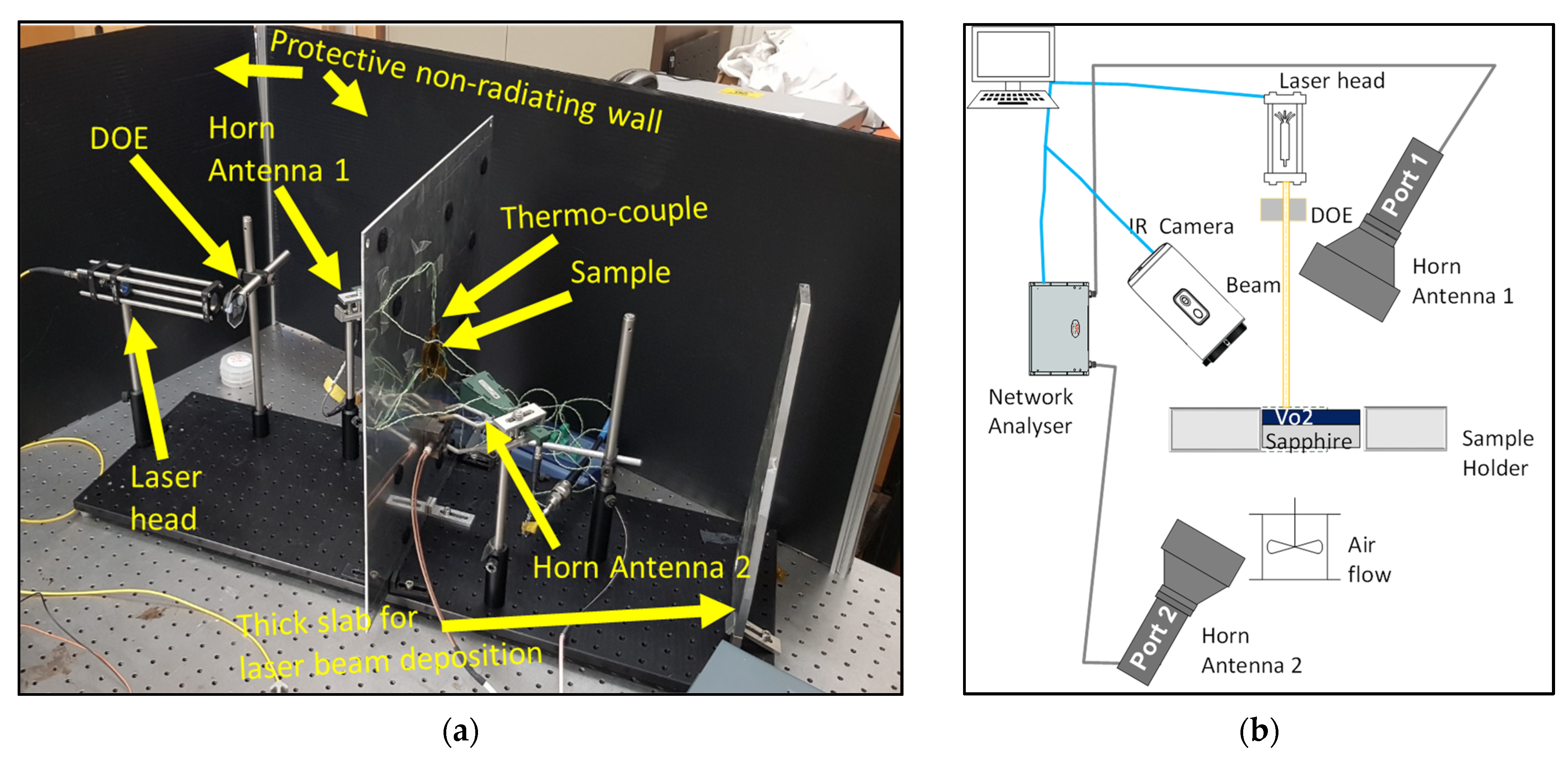
2.1. Measurement Setup

The measurement setup to form conductive patterns on the VO2 wafer and measure its transmission characteristics consisted of a free space arrangement with two broadband horn antennas over the frequency ranges of 2.5–5 GHz and 8–10 GHz and a metallic wall with a circular aperture of 5.08 cm diameter that acted as the sample holder. The setup dimensions are defined in [55] based on a half-power beamwidth to ensure the EM waves pass through the aperture. The distance between the antenna and sample, r, was more significant than the wavelength, λ = 0.14 m at 2 GHz, and the aperture.
A gated reflection load (G.R.L.) calibration was used with a metal plate containing an aperture to confine the resolution to the sample; two primary calibration standards are considered here. They include VNA calibration and free space calibration [56].
The network analyser calibration involved using short, open, load, and through (SOLT) standards that removed unwanted effects of cables and adaptors by shifting the plane of reference to the antennas. The calibration was performed at room temperature by using the Keysight 85052D calibration kit due to its broadband nature. Initially, this calibration kit works with coaxial setups; however, short, open, and load standards were inserted into the antenna connectors, which were connected for the through standard. The path losses were thus considered in the calibration. The remaining reflections, in the antennas and on the metal plate globally, were handled through post-process time-gating. The gate was defined by comparing the time domain responses of the empty fixture with the metal in the fixture: the only difference between them was due to the sample difference (Cu vs. air). All the other areas were filled by unwanted reflections that were thus suppressed. N5225A PNA from Agilent was used for all measurements, connected to two horn antennas through 3.5 mm connectors, as shown in Figure 1a,b.

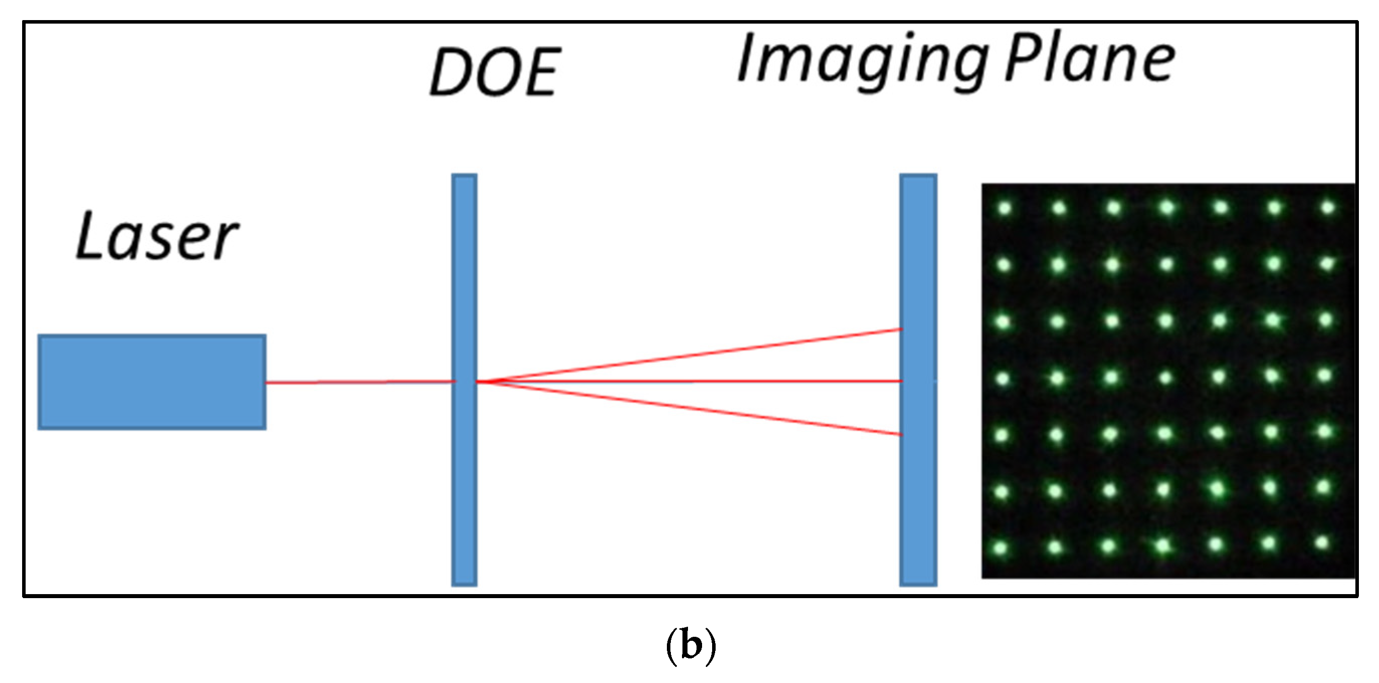
2.2. Phase Pattern Formation

The DOE is designed to operate in the Fresnel regime [57] using an iterative Fourier transform algorithm (IFTA) to generate the phase profiles. The algorithm shown in Figure 2a finds the phase of a propagating optical field between two parallel planes with known amplitudes of the fields [58]. The derived phase is then used to calculate the modulation function of the phase to produce a known far-field distribution from the illuminating beam. IFTA takes the amplitude of the image and the Fourier transform of the image (amplitude of the diffraction plane) as its inputs. The process recovers phase information of the Fourier transform and reconstructs the signal. At each iteration, the process alternates between the frequency and time domains using the input amplitudes to improve phase estimation [59,60].
The DOE was fabricated at the class-1000 cleanroom nanofabrication centre of the Heriot-Watt University through photolithography on a substrate of 1 mm thickness through reactive ion etching (RIE).
The 100 W EPS-Z SPI laser system used a maximum pulse energy of 0.7 mJ, a duration of 490 ns, and a repletion rate of 28 kHz for etching. The etch depth was optimised for 1064 nm with a minimum feature size of 5 µm and aperture of 1 mm for an optical output of a 1 × 32 array. The projected dipole size was augmented by changing the propagation distance between the DOE and imaging plane, as described in Figure 2b.
Figure 3a–c show the optical diffraction pattern of dipoles on the VO2 film at specified propagation distances, while Figure 3d–f show the thermal actuating laser beam diffraction pattern of the dipoles. The dipole designs consisted of unit cells at 3, 3.3, and 4 GHz projected on the VO2 film circular surface of 50.8 mm diameter. The unit cell designs were selected at lower frequencies to obtain larger dipoles due to undesirable signal rejections caused by the heat spread on the VO2 wafer because of the changing thermal conductivity. The propagation distances used were 57.5 cm for 39 mm by 2.9 mm at 3 GHz, 42.5 cm for 30 mm by 2.9 mm at 3.3 GHz, and 32.5 cm for 23 mm by 2.9 mm at 4 GHz.

3. Results

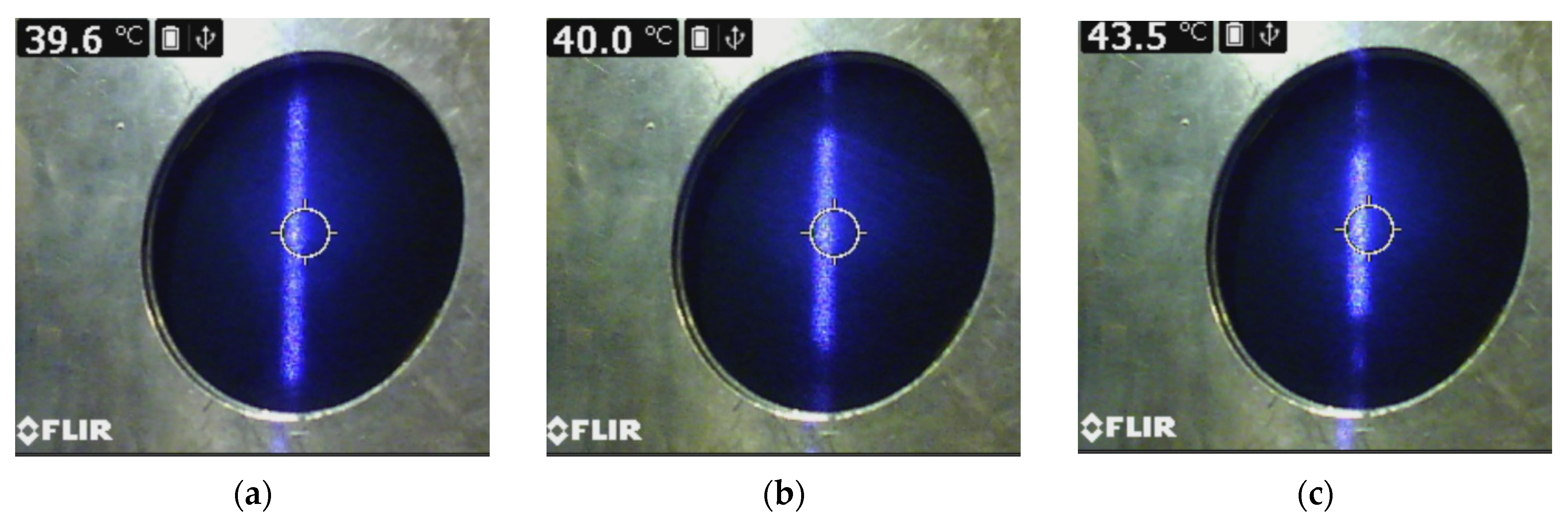
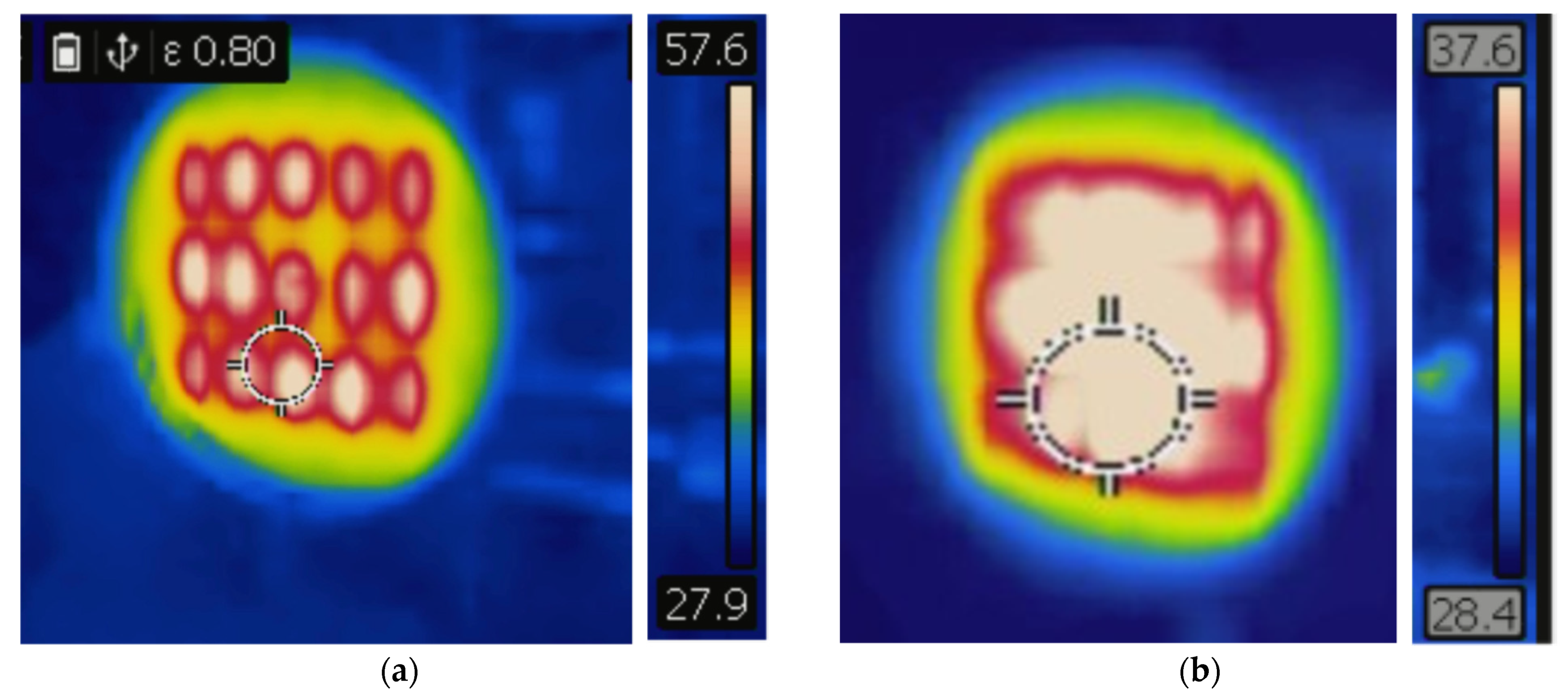
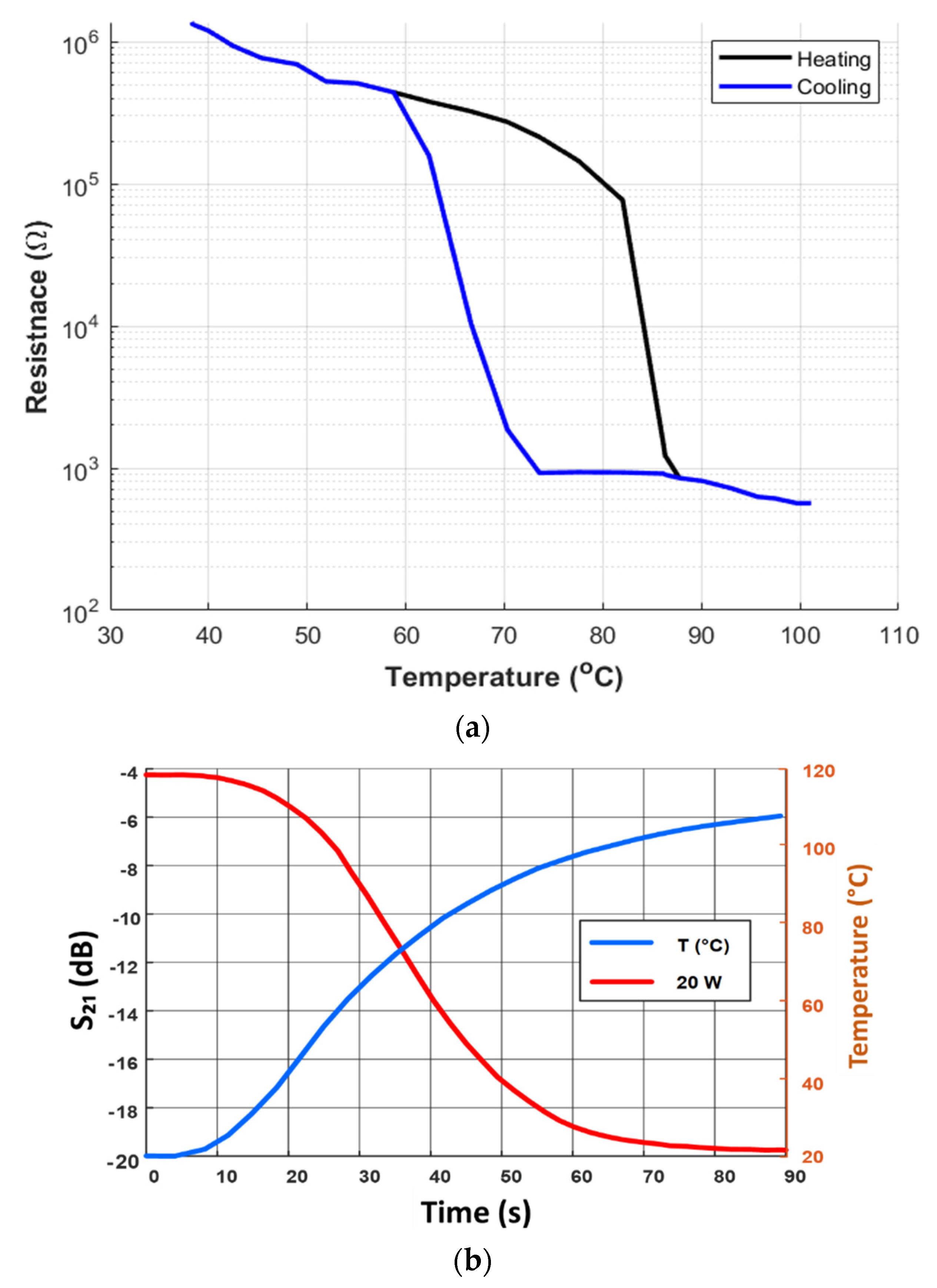
3.1. Material Thermal Property

In FSS applications, the individual elements are of the order of the operating wavelength λ/2, which resonates at the design frequency [61]. FSSs have periodicity equal to half the resonant frequency wavelength [62]. Any change in element dimensions will significantly affect the desired frequency response. The thermal conductivity of the VO2 wafer changes alongside the electrical conductivity during the transition, becoming more conductive, resulting in accumulated thermal profile changes [63,64,65]; therefore, it is essential to achieve good heat confinement to maintain the pattern of the projected DOE image on the wafer.
The film in Figure 4a–c consists of a 400 nm VO2 layer deposited on a 2-inch circular substrate of sapphire 275 µm thick. The wafer contains VO2 thin layer on a sapphire substrate. The VO2 layer has a thermal conductivity (K) of 0.9 W/mK at room temperature that increased to 2.5 W/mK after transition, specific heat capacity (c) of 656.31 J/KgK, and a density (ρ) of 4.58 g/cm3. The sapphire layer has a thermal conductivity of 23.1 W/mK, a specific heat capacity (c) of 761 J/KgK, and a density (ρ) of 3.98 g/cm3 as seen in Figure 4a.
The heat confinement of the dipole patterns is difficult to maintain at higher frequencies with smaller interelement spacing between unit cells due to the thermal conductivity associated with the phase transition. The confinement should have enough temperature difference between the dipoles of the FSS pattern and the interelement space between them such that only the dipole pattern attains the transition temperature. The heat confinement is improved by designing the unit cell with larger interelement spacing between the dipole elements and fewer elements.
The wafer is cooled from the back to improve the thermal confinement of the diffracted image, as shown in Figure 5. The cooling process transfers the heat transfer coefficient of the sample to the air surrounding it, thereby reducing the temperature in the sample. The airflow required to dissipate the heat is approximated when the density of the air is known [66]. The wafer temperature is monitored from the front with the FLIR E5-XT thermal imaging camera alongside K-type thermocouples at the back. The temperature distribution on the wafer profile is obtained from the thermal mapping of the camera, as shown in Figure 3 and Figure 6.
A pulsed wave (P.W.) laser scheme is used to heat the sample to the transition temperature. Before transition, the heat profile associated with the laser heating at transition temperature is less than 8 mm. On approaching the transition temperature, the heating profile expands to 8 mm. These changes are due to the increase in thermal conductivity during the IMT transition. The DOE image pattern in Figure 5 is unit cells modelled after FSS dipole surface patterns at 10 GHz. The proposed design is expected to give a passband response at the specific design frequencies.
Without cooling, undesirable signal rejections are obtained due to the heat spread on the VO2 wafer from the changing thermal conductivity, as shown in Figure 6. Figure 6 shows that heat expansion will not significantly alter the shape of the dipole at 110 °C. The heat expansion is attributed to the thermal conductivity of the base wafer on which the thin film is deposited. A base wafer with a lower thermal conductivity will be better suited for this application.

3.2. Microwave Properties

Dipole FSS arrays consist of unit cells periodically distributed on a substrate or a metallic sheet. These unit cells function as a radiation filter to manipulate waves [62].
VO2 thin film has demonstrated thermochromic properties as it undergoes IMT during the temperature rise. As the temperature increases, the transmission coefficient decreases while its reflective properties rise, as shown in Figure 7. This decrease is due to the rise in electrical conductivity. The results in Figure 7 show the entire film being heated from 20 °C to 110 °C, and a 16 dB change in transmission coefficient is observed. This property makes for an attractive reconfigurable FSS that is achieved by defocusing the beam to obtain various dipole patterns and using a diffuser to ensure uniform illumination.

3.2.1. Single Dipole Unit Cell

A single unit cell dipole is illuminated on the VO2 wafer matching a Cu unit cell of similar dimension. The length of the dipoles varies, as shown in Figure 8a,b. In Figure 9, the transmission frequency response of the VO2 wafer for dipoles of dimensions 30 mm × 2.9 mm at 3.3 GHz and 39 mm × 2.9 mm at 3 GHz are compared with Cu material of the exact dimensions on the same substrate.
In Figure 9, the 30 mm by 3 mm pattern heated to 110 °C generates a filtering frequency response with resonance slightly shifted to 3.4 GHz at 12 dB compared to the Cu dipole with a resonance at 3.6 GHz at 37 dB. The 39 mm by 3 mm pattern generates a filtering response of 7 dB at 3.1 GHz, while its Cu counterpart has a 21 dB response at 3.3 GHz. In both comparisons, the magnitude of the VO2 dipoles is three times less than the Cu dipoles, primarily due to the electrical conductivity of Cu. It washes away the diffracted pattern, which affects the transmission frequency response obtained due to the rise in thermal conductivity of the VO2 layer on going through IMT, although, by removing cooling, higher temperatures can be achieved.

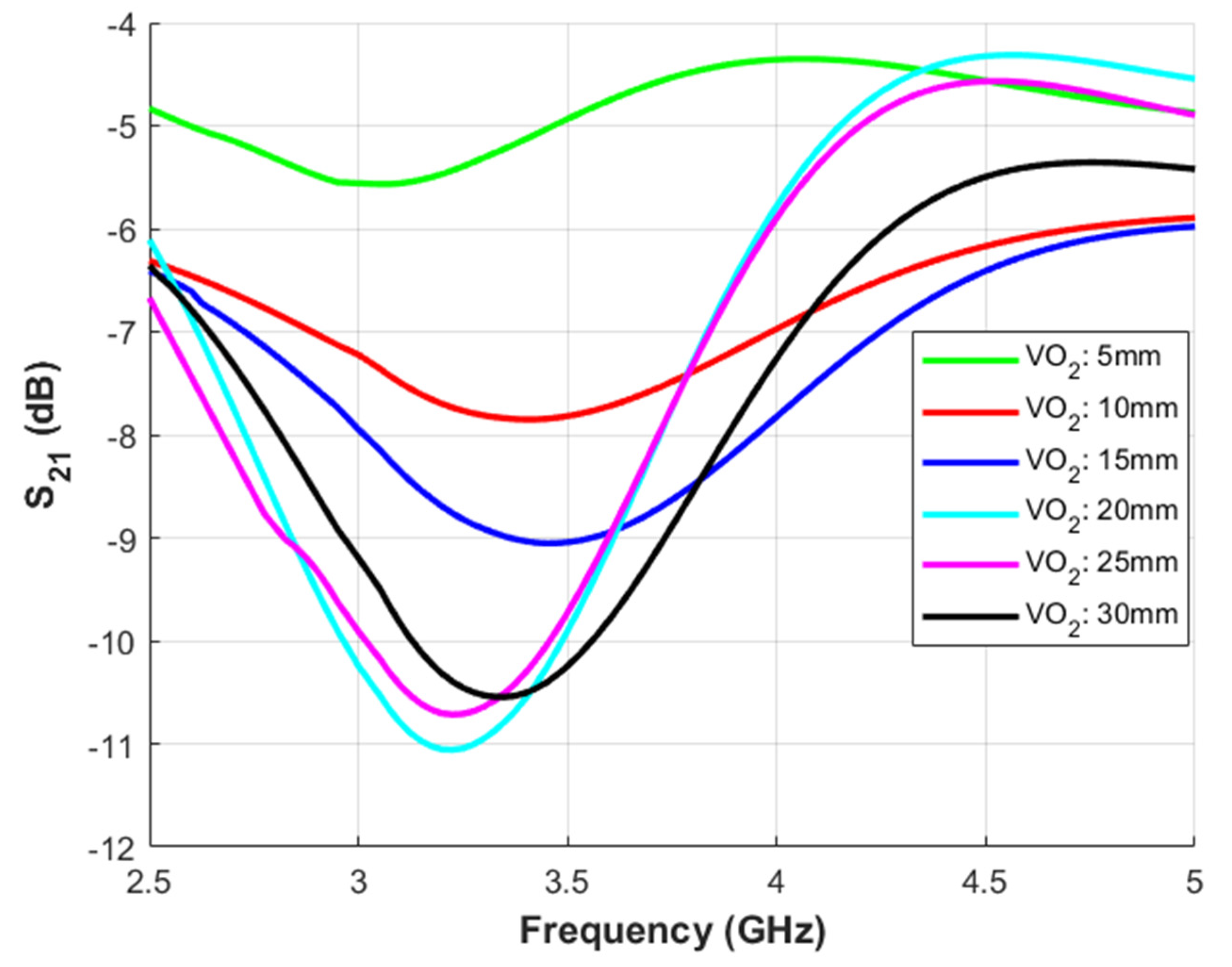
3.2.2. Two (Double) Dipole Unit Cell

Double dipole patterns were imprinted on the film, as shown in Figure 10. The dipoles are equal in length, L, and width, W, with a spacing, D, as shown in Figure 10 (inset). D varies from 5 mm to 30 mm compared to its Cu counterpart.
The magnitude of the transmission coefficient (S21) for VO2 double dipoles at different spacing, D, is shown in Figure 11. The frequency response of the dipoles stabilises by varying D with a fixed L and W of 39 mm and 3 mm, respectively. The resonance varied slightly from 3.2 to 3.4 GHz and became more defined with an increasing magnitude as the separation distance increased. This variance is due to the diffracted pattern moving closer to the designed dimensions and heat expansion caused by the changing thermal conductivity.
The magnitude of the transmission coefficient (S21) for VO2 double dipoles of spacings 25 and 30 mm compared to Cu is shown in Figure 12. The FSS response offers stable and identical transmission responses for both materials. From Figure 12, the VO2 dipoles with 25 mm spacing at −10 dB provides 1 GHz bandwidth of stopband. This response makes it attractive as a filter in communication. The rejection bandwidth increases as the spacing is varied.

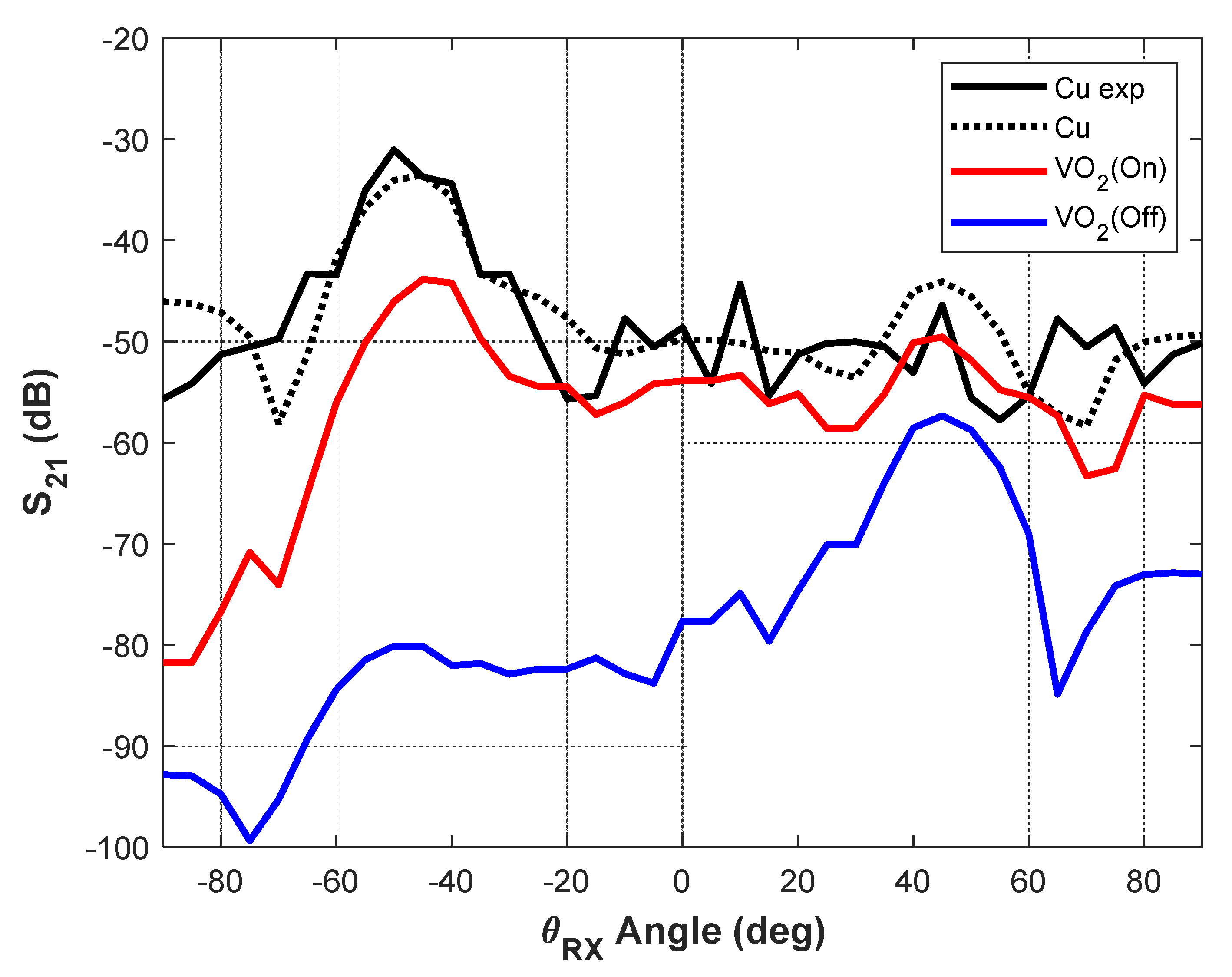
3.2.3. Full Dipole Array

The FSS shown in Figure 5a consists of a 3 × 5-unit cell arrangement at 10 GHz projected on the VO2 film circular surface of 50.8 mm diameter. The unit cell is made of dipoles of length, l(y) = 8.3 mm, width, w(x) = 3 mm, with the interelement spacings of dx(x) and dy(y) as 7.5 and 12 mm, respectively. This design is selected to fit an array on the VO2 surface. The dipole is used to demonstrate the proposed design of the FSS element in Figure 13. The proposed design employs variable state VO2 and is supported by a sapphire substrate with a thickness, h, of 420 µm and a dielectric constant, ε r , of 11. CST Microwave Studio software simulates the proposed FSS’s unit cell. The off-state (below transition temperature) of VO2 is modelled as “normal material” with a dielectric constant, ε r , of 34 and an electrical conductivity of 1.2 S/m. On the other hand, the on-state (above transition temperature) of VO2 is modelled as a lossy metal with an electrical conductivity of 1.2 × 10³ S/m.
The frequency domain solver was used for the simulation because it is appropriate for the simulation of a highly resonant structure, as well as acknowledging the examination of the FSS performance with variations in incident angle and polarisation. For the port assignment, the periodic boundary condition is set in horizontal and vertical directions, and the z-direction is set to open boundary conditions. The CST full Floquet port is used to simulate the presented FSS as an infinite array in the CST. This setting also helps to reduce the simulation load. Figure 14 depicts the proposed FSS’s simulated transmission response at the normal incident for both TE and TM polarisation.
The thermal nature of the VO2 layer is considered in the simulation model by varying the electrical conductivity across the unit cell structure in CST software. Figure 13 shows the simulation model and fabricated Cu FSS structure of the 10 GHz image projected in Figure 5a. The transmission coefficient for the dipole FSS array is represented in Figure 14. In this graph, the measured and simulated VO2 array responses are nearly the same as each other, with some slight variations. The resonant frequency for both the simulated and measured VO2 array is 10.5 GHz, with the simulated response having a sharper transmission coefficient of 16 dB, while the measured response has a broader result of 13 dB across 9.5–10.5 GHz. On the other hand, the response of Cu FSS shows the transmission coefficients of −24 dB and −22 dB at 9.6 and 9.9 GHz of resonant frequency, respectively.
The discrepancy between Cu and VO2, apart from the former’s higher conductivity value, is due to heat expansion. The heat expansion is maintained enough to form dipoles on the VO2 film, resulting in a filtering effect at 9.5–10.5 GHz; however, the heating still raises the global sample temperature even at the interelement spaces surrounding the dipole elements, which leads to a broader transmission curve and lowers the overall response. This temperature change is evident in the value between the lowest and highest S21 values of VO2 and Cu.
Figure 14 proves that VO2 has the potential to be used in reconfigurable devices. By moving to lower frequencies, the unit cell’s size increases, making it easier to contain the heat expansion. The cost and technology restrictions on the deposition of VO2 thin film make producing larger FSS array designs more challenging.
Radar cross-section (RCS) measurements were carried out on a fabricated FSS Cu array reflector at 14 GHz. The unit cell properties are used as a reference to analyse and estimate VO2 array response [4], as shown in Figure 15. The Cu simulation is matched to measurement results and compared to the VO2 array response in CST studio.
The bistatic RCS for TE polarised waves at an incidence angle of 45° is obtained using a finite array with 10 × 28-unit cells with size of 18 × 44 cm2, as illustrated in Figure 16. The RCS for Cu array reflects the incident signal to the impinging direction at −31 dB, while the VO2 array in the on-state reflects at −45 dB. The discrepancy of the magnitude of reflection can be attributed partly to the conductor and dielectric losses exhibited by the array (the heated VO2 is not a perfect electric conductor) and partly to design imperfections. It is highlighted that the angle of reflection remains unchanged.

4. Conclusions

A reconfigurable selective surface using the thermochromic property of VO2 material for electromagnetic wave manipulation was proposed. The use of VO2 film as an FSS array for reconfigurable spatial filtering is demonstrated. Using laser heating and a DOE lens, we have demonstrated that it can project FSS dipoles onto the VO2 surface to produce frequency-selective surfaces via adequate heat management. The proposed technique will offer a solution for reconfigurable metamaterial applications.
Moreover, it has been shown that the transmission response of the VO2 FSS is the same as that of a Cu FSS, particularly at lower frequencies with more giant FSS unit cells, where the dipole image has better thermal management to maintain the FSS periodicity. The results are further validated by simulation and a fabricated FSS prototype, which were in good agreement. Extension of the proposed solution to reflective surfaces can readily be made using the same design concepts with an adequate heat management scheme. Beyond the FSS application, the proposed concept is suitable for several other quasi-optical and quantum applications where polarisation-selective surfaces are required.

Author Contributions

Conceptualisation, D.E.A., G.G. and D.H.; methodology, Q.A., A.D. and C.R.; software, Q.A.; validation, Q.A., A.D. and C.R.; formal analysis, Q.A. and A.D.; investigation, Q.A., A.D. and C.R.; resources, D.E.A., G.G. and D.H.; data curation, Q.A.; writing—original draft preparation, Q.A.; writing—review and editing, Q.A., A.D., C.R., G.J., N.S., A.S., G.G., D.H. and D.E.A.; visualisation, A.D.; supervision, D.E.A., G.G. and D.H.; project administration, D.E.A., G.G. and D.H.; funding acquisition, D.E.A., G.G. and D.H. All authors have read and agreed to the published version of the manuscript.

Funding

This research was partly supported by the Defence and Security Accelerator project #ACC6003961 and the European H2020 Marie Skłodowska-Curie Individual Fellowship (MSCA-IF) grant #840854 (VisionRF).

Data Availability Statement

Not applicable.

Conflicts of Interest

The authors declare no conflict of interest.

References

  1. ISO-ISO 12567-1:2000-Thermal Performance of Windows and Doors—Determination of Thermal Transmittance by Hot Box Method—Part 1: Complete Windows and Doors. Available online: https://www.iso.org/standard/2533.html (accessed on 11 August 2021).
  2. Handbook of Energy Efficiency in Buildings; Elsevier: Amsterdam, The Netherlands, 2019. [CrossRef]
  3. Karlessi, T.; Santamouris, M.; Apostolakis, K.; Synnefa, A.; Livada, I. Development and testing of thermochromic coatings for buildings and urban structures. Sol. Energy 2009, 83, 538–551. [Google Scholar] [CrossRef]
  4. Doumanis, E.; Goussetis, G.; Papageorgiou, G.; Fusco, V.; Cahill, R.; Linton, D. Design of Engineered Reflectors for Radar Cross Section Modification. IEEE Trans. Antennas Propag. 2012, 61, 232–239. [Google Scholar] [CrossRef]
  5. Pendry, J.B.; Schurig, D.; Smith, D.R. Controlling Electromagnetic Fields. Science 2006, 312, 1780–1782. [Google Scholar] [CrossRef] [PubMed] [Green Version]
  6. Chen, H.; Chan, C.T.; Sheng, P. Transformation optics and metamaterials. Nat. Mater. 2010, 9, 387–396. [Google Scholar] [CrossRef] [PubMed]
  7. Schurig, D.; Mock, J.J.; Justice, B.J.; Cummer, S.A.; Pendry, J.B.; Starr, A.F.; Smith, D.R. Metamaterial Electromagnetic Cloak at Microwave Frequencies. Science 2006, 314, 977–980. [Google Scholar] [CrossRef] [PubMed] [Green Version]
  8. Gric, T. Spoof plasmons in corrugated transparent conducting oxides. J. Electromagn. Waves Appl. 2016, 30, 721–727. [Google Scholar] [CrossRef]
  9. Anagnostou, D.E.; Torres, D.; Teeslink, T.S.; Sepulveda, N. Vanadium Dioxide for Reconfigurable Antennas and Microwave Devices: Enabling RF Reconfigurability through Smart Materials. IEEE Antennas Propag. Mag. 2020, 62, 58–73. [Google Scholar] [CrossRef]
  10. Anagnostou, D.E.; Teeslink, T.S.; Torres, D.; Sepulveda, N. Vanadium dioxide reconfigurable slot antenna. In Proceedings of the 2016 IEEE International Symposium on Antennas and Propagation (APSURSI), Fajardo, PR, USA, 26 June–1 July 2016; pp. 1055–1056. [Google Scholar] [CrossRef]
  11. Teeslink, T.S.; Torres, D.; Ebel, J.L.; Sepulveda, N.; Anagnostou, D.E. Reconfigurable Bowtie Antenna Using Metal-Insulator Transition in Vanadium Dioxide. IEEE Antennas Wirel. Propag. Lett. 2015, 14, 1381–1384. [Google Scholar] [CrossRef]
  12. Casu, E.A.; Ionescu, A.M.; Oliva, N.; Cavalieri, M.; Muller, A.A.; Fumarola, A.; Vitale, W.A.; Krammer, A.; Schuler, A.; Fernandez-Bolanos, M. Tunable RF Phase Shifters Based on Vanadium Dioxide Metal Insulator Transition. IEEE J. Electron. Devices Soc. 2018, 6, 965–971. [Google Scholar] [CrossRef]
  13. Gerislioglu, B.; Ahmadivand, A.; Karabiyik, M.; Sinha, R.; Pala, N. VO2-Based Reconfigurable Antenna Platform with Addressable Microheater Matrix. Adv. Electron. Mater. 2017, 3, 1700170. [Google Scholar] [CrossRef]
  14. Earl, S.K.; James, T.D.; Davis, T.J.; McCallum, J.C.; Marvel, R.E.; Haglund, R.F.; Roberts, A. Tunable optical antennas enabled by the phase transition in vanadium dioxide. Opt. Express 2013, 21, 27503–27508. [Google Scholar] [CrossRef] [PubMed]
  15. Figueroa, J.; Cao, Y.; Dsouza, H.; Pastrana, J.; Sepúlveda, N. A Simplified Approach for Obtaining Optical Properties of VO2 Thin Films, and Demonstration of Infrared Shape-Shifting Devices. Adv. Mater. Technol. 2019, 4, 1800599. [Google Scholar] [CrossRef]
  16. Figueroa, J.; Dsouza, H.; Pastrana, J.; Torres, D.; Hall, H.; Leedy, K.; Sepúlveda, N. VO2-based micro-electro-mechanical tunable optical shutter and modulator. Opt. Express 2021, 29, 25242. [Google Scholar] [CrossRef] [PubMed]
  17. Cui, T.J.; Qi, M.Q.; Wan, X.; Zhao, J.; Cheng, Q. Coding metamaterials, digital metamaterials and programmable metamaterials. Light. Sci. Appl. 2014, 3, e218. [Google Scholar] [CrossRef] [Green Version]
  18. Shao, L.; Zhu, W.; Leonov, M.Y.; Rukhlenko, I.D. Dielectric 2-bit coding metasurface for electromagnetic wave manipulation. J. Appl. Phys. 2019, 125, 203101. [Google Scholar] [CrossRef]
  19. Cui, T.-J.; Liu, S.; Li, L.-L. Information entropy of coding metasurface. Light. Sci. Appl. 2016, 5, e16172. [Google Scholar] [CrossRef] [Green Version]
  20. Zhang, L.; Liu, S.; Li, L.; Cui, T.J. Spin-Controlled Multiple Pencil Beams and Vortex Beams with Different Polarizations Generated by Pancharatnam-Berry Coding Metasurfaces. ACS Appl. Mater. Interfaces 2017, 9, 36447–36455. [Google Scholar] [CrossRef]
  21. Shabanpour, J.; Beyraghi, S.; Cheldavi, A. Ultrafast reprogrammable multifunctional vanadium-dioxide-assisted metasurface for dynamic THz wavefront engineering. Sci. Rep. 2020, 10, 8950. [Google Scholar] [CrossRef]
  22. Ding, F.; Yang, Y.; Bozhevolnyi, S.I. Dynamic Metasurfaces Using Phase-Change Chalcogenides. Adv. Opt. Mater. 2019, 7, 1801709. [Google Scholar] [CrossRef] [Green Version]
  23. Xu, J.; Yang, R.; Fan, Y.; Fu, Q.; Zhang, F. A Review of Tunable Electromagnetic Metamaterials With Anisotropic Liquid Crystals. Front. Phys. 2021, 9, 633104. [Google Scholar] [CrossRef]
  24. Che, Y.; Wang, X.; Song, Q.; Zhu, Y.; Xiao, S. Tunable optical metasurfaces enabled by multiple modulation mechanisms. Nanophotonics 2020, 9, 4407–4431. [Google Scholar] [CrossRef]
  25. Howes, A.; Zhu, Z.; Curie, D.; Avila, J.R.; Wheeler, V.D.; Haglund, R.F.; Valentine, J.G. Optical Limiting Based on Huygens’ Metasurfaces. Nano Lett. 2020, 20, 4638–4644. [Google Scholar] [CrossRef] [PubMed]
  26. Wang, X.; Ma, C.; Xiao, L.; Li, X.; Yu, J.; Xiao, B. Dynamically tunable broadband absorber/reflector based ongraphene and VO2 metamaterials. Appl. Opt. 2022, 61, 1646–1651. [Google Scholar] [CrossRef]
  27. Tripathi, A.; John, J.; Kruk, S.; Zhang, Z.; Nguyen, H.S.; Berguiga, L.; Romeo, P.R.; Orobtchouk, R.; Ramanathan, S.; Kivshar, Y.; et al. Tunable Mie-Resonant Dielectric Metasurfaces Based on VO2 Phase-Transition Materials. ACS Photon 2021, 8, 1206–1213. [Google Scholar] [CrossRef]
  28. Zhang, R.; Fu, Q.S.; Yin, C.Y.; Li, C.; Chen, X.H.; Qian, G.; Lu, C.L.; Yuan, S.L.; Zhao, X.J.; Tao, H.Z. Understanding of metal-insulator transition in VO2 based on experimental and theoretical investigations of magnetic features. Sci. Rep. 2018, 8, 17093. [Google Scholar] [CrossRef] [Green Version]
  29. Liou, Y.-J.; Huang, W.-J. High Temperature Phase Transitions of Graphene Oxide Paper from Graphite Oxide Solution. J. Mater. Sci. Technol. 2014, 30, 1088–1091. [Google Scholar] [CrossRef]
  30. Vinod, E.M.; Ramesh, K.; Sangunni, K.S. Structural transition and enhanced phase transition properties of Se doped Ge2Sb2Te5 alloys. Sci. Rep. 2015, 5, srep08050. [Google Scholar] [CrossRef] [Green Version]
  31. Gaebler, A.; Moessinger, A.; Goelden, F.; Manabe, A.; Goebel, M.; Follmann, R.; Koether, D.; Modes, C.; Kipka, A.; Deckelmann, M.; et al. Liquid Crystal-Reconfigurable Antenna Concepts for Space Applications at Microwave and Millimeter Waves. Int. J. Antennas Propag. 2009, 2009, 876989. [Google Scholar] [CrossRef]
  32. Laverock, J.; Kittiwatanakul, S.; Zakharov, A.A.; Niu, Y.R.; Chen, B.; Wolf, S.A.; Lu, J.W.; Smith, K.E. Direct Observation of Decoupled Structural and Electronic Transitions and an Ambient Pressure Monocliniclike Metallic Phase of VO2. Phys. Rev. Lett. 2014, 113, 216402. [Google Scholar] [CrossRef] [Green Version]
  33. Lv, Y.-H.; Ding, X.; Wang, B.-Z.; Anagnostou, D.E. Scanning Range Expansion of Planar Phased Arrays Using Metasurfaces. IEEE Trans. Antennas Propag. 2020, 68, 1402–1410. [Google Scholar] [CrossRef]
  34. Muskens, O.; Bergamini, L.; Wang, Y.; Gaskell, J.M.; Zabala, N.; de Groot, C.; Sheel, D.W.; Aizpurua, J. Antenna-assisted picosecond control of nanoscale phase transition in vanadium dioxide. Light. Sci. Appl. 2016, 5, e16173. [Google Scholar] [CrossRef] [Green Version]
  35. Earl, S.K.; James, T.D.; Gómez, D.E.; Marvel, R.E.; Haglund, R.F., Jr.; Roberts, A. Switchable polarization rotation of visible light using a plasmonic metasurface. APL Photon 2017, 2, 016103. [Google Scholar] [CrossRef]
  36. Shao, Z.; Cao, X.; Luo, H.; Jin, P. Recent progress in the phase-transition mechanism and modulation of vanadium dioxide materials. NPG Asia Mater. 2018, 10, 581–605. [Google Scholar] [CrossRef] [Green Version]
  37. Cueff, S.; John, J.; Zhang, Z.; Parra, J.; Sun, J.; Orobtchouk, R.; Ramanathan, S.; Sanchis, P. VO2 nanophotonics. APL Photon 2020, 5, 110901. [Google Scholar] [CrossRef]
  38. Kats, M.A.; Sharma, D.; Lin, J.; Genevet, P.; Blanchard, R.; Yang, Z.; Qazilbash, M.M.; Basov, D.N.; Ramanathan, S.; Capasso, F. Ultra-thin perfect absorber employing a tunable phase change material. Appl. Phys. Lett. 2012, 101, 221101. [Google Scholar] [CrossRef] [Green Version]
  39. Rensberg, J.; Zhou, Y.; Richter, S.; Wan, C.; Zhang, S.; Schöppe, P.; Schmidt-Grund, R.; Ramanathan, S.; Capasso, F.; Kats, M.A.; et al. Epsilon-Near-Zero Substrate Engineering for Ultrathin-Film Perfect Absorbers. Phys. Rev. Appl. 2017, 8, 014009. [Google Scholar] [CrossRef] [Green Version]
  40. Kats, M.A.; Blanchard, R.; Zhang, S.; Genevet, P.; Ko, C.; Ramanathan, S.; Capasso, F. Vanadium Dioxide as a Natural Disordered Metamaterial: Perfect Thermal Emission and Large Broadband Negative Differential Thermal Emittance. Phys. Rev. X 2013, 3, 041004. [Google Scholar] [CrossRef] [Green Version]
  41. Bouyge, D.; Crunteanu, A.; Orlianges, J.-C.; Passerieux, D.; Champeaux, C.; Catherinot, A.; Velez, A.; Bonache, J.; Martin, F.; Blondy, P. Reconfigurable bandpass filter based on split ring resonators and vanadium dioxide (VO2) microwave switches. In Proceedings of the 2009 Asia Pacific Microwave Conference 2009, Singapore, 7–10 December 2009; pp. 2332–2335. [Google Scholar] [CrossRef]
  42. Liu, L.; Kang, L.; Mayer, T.S.; Werner, D.H. Hybrid metamaterials for electrically triggered multifunctional control. Nat. Commun. 2016, 7, 13236. [Google Scholar] [CrossRef]
  43. Zhu, Z.; Evans, P.G.; Haglund, R.F., Jr.; Valentine, J.G. Dynamically Reconfigurable Metadevice Employing Nanostructured Phase-Change Materials. Nano Lett. 2017, 17, 4881–4885. [Google Scholar] [CrossRef]
  44. Kim, Y.; Wu, P.C.; Sokhoyan, R.; Mauser, K.A.; Glaudell, R.; Shirmanesh, G.K.; Atwater, H.A. Phase Modulation with Electrically Tunable Vanadium Dioxide Phase-Change Metasurfaces. Nano Lett. 2019, 19, 3961–3968. [Google Scholar] [CrossRef] [Green Version]
  45. Wang, N.; Peh, Y.K.; Magdassi, S.; Long, Y. Surface engineering on continuous VO2 thin films to improve thermochromic properties: Top-down acid etching and bottom-up self-patterning. J. Colloid Interface Sci. 2017, 512, 529–535. [Google Scholar] [CrossRef] [PubMed]
  46. Dong, K.; Hong, S.; Deng, Y.; Ma, H.; Li, J.; Wang, X.; Yeo, J.; Wang, L.; Lou, S.; Tom, K.B.; et al. A Lithography-Free and Field-Programmable Photonic Metacanvas. Adv. Mater. 2017, 30, 1703878. [Google Scholar] [CrossRef] [PubMed]
  47. Sanphuang, V.; Ghalichechian, N.; Nahar, N.K.; Volakis, J.L. Equivalent circuit for VO2 phase change material film in reconfigurable frequency selective surfaces. Appl. Phys. Lett. 2015, 107, 253106. [Google Scholar] [CrossRef]
  48. Newton, L.; Nahar, N.K. Equivalent Circuit Model for Reconfigurable Far-Infrared Filter Employing Vanadium Dioxide. In Proceedings of the 2019 IEEE International Symposium on Antennas and Propagation and USNC-URSI Radio Science Meeting, Atlanta, GA, USA, 7–12 July 2019; pp. 513–514. [Google Scholar] [CrossRef]
  49. Sanphuang, V.; Ghalichechian, N.; Nahar, N.K.; Volakis, J.L. Reconfigurable THz Filters Using Phase-Change Material and Integrated Heater. IEEE Trans. Terahertz Sci. Technol. 2016, 6, 583–591. [Google Scholar] [CrossRef]
  50. Chen, Y.; Cheng, J.; Liang, C. Switchable Terahertz Band-Pass/Band-Stop Filter Enabled by Hybrid Vanadium Dioxide Metamaterial. Adv. Condens. Matter Phys. 2020, 2020, 3902835. [Google Scholar] [CrossRef]
  51. Nouman, M.T.; Hwang, J.H.; Faiyaz, M.; Lee, K.-J.; Noh, D.-Y.; Jang, J.-H. Vanadium dioxide based frequency tunable metasurface filters for realizing reconfigurable terahertz optical phase and polarization control. Opt. Express 2018, 26, 12922–12929. [Google Scholar] [CrossRef]
  52. Polozov, V.; Maklakov, S.S.; Mishin, A.; Petrov, D.; Baskov, K.; Politiko, A.; Chistyaev, V.; Semenenko, V.; Kisel, V. Thermally Tunable Frequency-Selective Surface Based on VO2 Thin Film. Phys. Status Solidi (a) 2020, 217, 2000452. [Google Scholar] [CrossRef]
  53. Vitale, W.A.; Petit, L.; Moldovan, C.F.; Fernández-Bolaños, M.; Paone, A.; Schüler, A.; Ionescu, A.M. Electrothermal actuation of vanadium dioxide for tunable capacitors and microwave filters with integrated microheaters. Sens. Actuators A Phys. 2016, 241, 245–253. [Google Scholar] [CrossRef]
  54. Yang, S.; Li, W.; Vaseem, M.; Shamim, A. Additively Manufactured Dual-Mode Reconfigurable Filter Employing VO2-Based Switches. IEEE Trans. Compon. Packag. Manuf. Technol. 2020, 10, 1738–1744. [Google Scholar] [CrossRef]
  55. Gonçalves, F.J.F.; Pinto, A.G.M.; Mesquita, R.C.; Silva, E.J.; Brancaccio, A. Free-Space Materials Characterization by Reflection and Transmission Measurements using Frequency-by-Frequency and Multi-Frequency Algorithms. Electronics 2018, 7, 260. [Google Scholar] [CrossRef] [Green Version]
  56. Dhondt, G.; De Zutter, D.; Martens, L. An improved free-space technique modelling for measuring dielectric properties of materials. In Proceedings of the IEEE Antennas and Propagation Society International Symposium, Baltimore, MD, USA, 21–26 July 2002; Volume 1, pp. 180–183. [Google Scholar] [CrossRef]
  57. Kim, G.; Domínguez-Caballero, J.A.; Menon, R. Design and analysis of multi-wavelength diffractive optics. Opt. Express 2012, 20, 2814–2823. [Google Scholar] [CrossRef] [PubMed]
  58. Wyrowski, F.; Bryngdahl, O. Iterative Fourier-transform algorithm applied to computer holography. J. Opt. Soc. Am. A 1988, 5, 1058–1065. [Google Scholar] [CrossRef]
  59. Gerhberg, R.W.; Saxton, W.O. A practical algorithm for the determination of phase from image and diffraction plane picture. Optik 1972, 35, 237–246. [Google Scholar]
  60. Whyte, G.; Courtial, J. Experimental demonstration of holographic three-dimensional light shaping using a Gerchberg–Saxton algorithm. New J. Phys. 2005, 7, 117. [Google Scholar] [CrossRef]
  61. Anwar, R.S.; Mao, L.; Ning, H. Frequency Selective Surfaces: A Review. Appl. Sci. 2018, 8, 1689. [Google Scholar] [CrossRef] [Green Version]
  62. Glybovski, S.B.; Tretyakov, S.A.; Belov, P.A.; Kivshar, Y.S.; Simovski, C.R. Metasurfaces: From microwaves to visible. Phys. Rep. 2016, 634, 1–72. [Google Scholar] [CrossRef]
  63. Andreev, V.N.; Chudnovskii, F.A.; Petrov, A.V.; Terukov, E.I. Thermal conductivity of VO2, V3O5, and V2O3. Phys. Status Solidi 1978, 48, K153–K156. [Google Scholar] [CrossRef]
  64. Oh, D.-W.; Ko, C.; Ramanathan, S.; Cahill, D.G. Thermal conductivity and dynamic heat capacity across the metal-insulator transition in thin film VO2. Appl. Phys. Lett. 2010, 96, 151906. [Google Scholar] [CrossRef]
  65. Li, D.; Wang, Q.; Xu, X. Thermal Conductivity of VO2 Nanowires at Metal-Insulator Transition Temperature. Nanomaterials 2021, 11, 2428. [Google Scholar] [CrossRef]
  66. Steinberg, D.S. Cooling Techniques for Electronic Equipment; Wiley: New York, NY, USA, 1991; p. 483. [Google Scholar]
Figure 1. (a) Experimental setup in the lab. (b) Schematic of the measurement setup. (c) Elevated view of experimental setup in the lab.
Electronics 11 04099 g001aElectronics 11 04099 g001b
Figure 2. (a) Flowchart of DOE formation through phase retrieval. φ , A 0 are estimates of the image phase and amplitude respectively. The Fourier transform of image plane, A 0 e i φ is used to recover the output plane, A e i ϕ . The output plane calculated from the diffraction pattern is estimated to the desired Fourier transform output intensity, A m e i ϕ . The estimate of the Fourier transform is then inverse Fourier transformed to A s e i φ . The IFT signal must is changed if the new estimate of the transform does not satisfies the desired output constraints then the whole process is repeated until both the Fourier constraint and output constraint are satisfied. (b) Schematic of phase pattern formation with DOE.
Electronics 11 04099 g002aElectronics 11 04099 g002b
Figure 3. The dipole dimensions at varying propagation distances: (a) Infrared image of the diffraction pattern for 57.5 cm for a 39 × 2.9 mm dipole; (b) Infrared image of the diffraction pattern for 42.5 cm for a 30 × 2.9 mm dipole; (c) Infrared image of the diffraction pattern for 32.5 cm for a 23 × 2.9 mm dipole; (d) thermal image with laser for (a); (e) thermal image with laser for (b); (f) thermal image with laser for diffraction pattern for 32.5 cm for a 23 × 2.9 mm dipole.
Electronics 11 04099 g003aElectronics 11 04099 g003b
Figure 4. (a) Estimated thermal effusivity of the wafer containing a 2-inch circular VO2 thin layer with 400 nm thickness on 275 µm sapphire substrate. (b) VO2 sample. (c) The thermal infrared image is taken from the FLIR camera of the VO2 sample.
Electronics 11 04099 g004
Figure 5. Thermal image of dipole array through Pulse Wave: (a) with cooling; (b) no cooling.
Electronics 11 04099 g005
Figure 6. The temperature distribution of unit cells on the sapphire wafer with and without cooling.
Electronics 11 04099 g006
Figure 7. (a) Measured electrical resistance of VO2 thin film during the heating and cooling phase. (b) Measured transmission characteristics of full wafer heating attenuated by 16 dB at 10 GHz.
Electronics 11 04099 g007
Figure 8. Captured images of laser projected single dipole pattern with dimensions: (a) 30 mm × 2.9 mm (~3.3 GHz); (b) 39 mm × 2.9 mm (~3 GHz).
Electronics 11 04099 g008
Figure 9. The graph of the measured transmission coefficient of single dipole element of VO2 and Cu for lengths 30 and 39 mm.
Electronics 11 04099 g009
Figure 10. Captured laser image of thermal profile of double dipole pattern on VO2 over sapphire wafer during heating. Inset: geometry of double dipoles showing the length, L, width, W, and spacing, D.
Electronics 11 04099 g010
Figure 11. The graph of the measured transmission coefficient of the double diffracted dipole pattern on VO2 over sapphire wafer with varying separation distance at L = 39 mm and W = 3 mm.
Electronics 11 04099 g011
Figure 12. The graph of the measured transmission coefficient of VO2 and Cu double dipoles for separations of 25 mm and 30 mm.
Electronics 11 04099 g012
Figure 13. FSS design of: (a) VO2 showing a hot state (red) modelled as a lossy metal with an electrical conductivity of 1.2 × 10³ S/m and cold state (black) modelled as “normal material” with a dielectric constant, ε r , of 34 and an electrical conductivity of 1.2 S/m in CST software; (b) Cu FSS structure on the sample holder; (c) Cu FSS array on a glass substrate; (d) Modelling FSS structure on sapphire in CST software.
Electronics 11 04099 g013
Figure 14. Graph of the measured and simulated transmission coefficient of the FSS dipole array.
Electronics 11 04099 g014
Figure 15. Bistatic RCS measurement setup with fixed transmitter (Tx).
Electronics 11 04099 g015
Figure 16. Graph of the bistatic RCS responses of the manufactured and evaluated FSS reflectors with fixed Tx at −45°.
Electronics 11 04099 g016
Publisher’s Note: MDPI stays neutral with regard to jurisdictional claims in published maps and institutional affiliations.

