Article

An Optical Encoder Chip with Area Compensation

School of Microelectronics, Tianjin University, Tianjin 300072, China
*
Author to whom correspondence should be addressed.
Electronics 2022, 11(23), 3997; https://doi.org/10.3390/electronics11233997
Submission received: 1 November 2022 / Revised: 28 November 2022 / Accepted: 30 November 2022 / Published: 2 December 2022
(This article belongs to the Section Semiconductor Devices)

Abstract

:
A photodiode area-compensation method based on light intensity distribution characteristics is introduced to solve the problem of the hybrid optical encoder’s inconsistent absolute code output signals. This method performs area compensation of different degrees according to the irradiance received by the photodiodes at different positions, thus achieving the consistency of output signals and reducing the bit error rate of absolute code signals. Based on the 0.35 μ m m CMOS process, a four-channel photodiode array chip for a reflective hybrid optical encoder was designed. Moreover, the absolute code photodiode arrays were designed with area compensation. The test results show that the square wave duty cycle error of the output signals is less than 2% when the LED light source works normally. When the LED working current changes by ±2.85 mA, the output signal’s square wave duty cycle error is less than 3.1%. In each case, the square wave duty cycle error of the output signals is small, so it can be seen that the area compensation method based on light intensity distribution can achieve good consistency of the output signal. The chip has been taped and packaged, and the chip area is 21.45 mm 2 .

1. Introduction

An optical encoder is a precision optical instrument that converts mechanical geometric displacements into electrical signals through photoelectric conversion technology and is widely used in many fields, such as robots, avionics systems, and automotive sensors [1,2,3]. According to their imaging principle, optical encoders can usually be divided into transmission and reflection types. The imaging principle of the transmissive optical encoder is based on the Moiré effect, and this optical encoder has strict requirements on the line width of the grating and the position of the two gratings [4]. Reflective optical encoders are imaged based on the diffraction principle and have better accuracy, higher resolution, and larger installation tolerances [5]. According to their working principles and coding methods, optical encoders can usually be divided into incremental, absolute, and hybrid types. Incremental encoders use output signals to obtain relative position information [6], but suffer from cumulative errors and data loss after power failure. Absolute encoders use digital coding to obtain absolute position information [7,8], but the higher the number of coding bits, the larger the size, which makes it difficult to realize miniaturization. The code disk of the hybrid optical encoder combines incremental code tracks and absolute code tracks [9], which can not only measure the absolute position but also subdivide the angle. Thus, the hybrid optical encoder ensures miniaturization and increases resolution simultaneously.
In the previous research on the output signals of the optical encoder, the focus was mainly on improving the sinusoidal property of the incremental signal [10,11,12,13,14] and reducing the error of the signal [15,16,17]. However, there was little research on converting the photocurrent of absolute code into the correct digital signal. The digitization process of the absolute code signals is usually completed by comparators [18]. When multiple absolute codes are output by multiple photodiodes in parallel, the photocurrent generated in different pathways is different due to the different distance between the photodiodes and the light source and the different illumination intensity. In order to read out the absolute code accurately, the common method is to design the amplifiers for different readout channels with adjustable gain [19] or set different reference levels for the comparators for different channels [20]. These two methods not only make the following processing circuit more complicated but also increase the difficulty of debugging. There are also studies using digital self-calibration [21], which used digital circuits to dynamically calculate the readout signal in the channel to adjust the reference level of the comparator continuously. However, this method increases the complexity of the digital processing circuit, and it is not easy to implement when there are many parallel channels.
In this paper, a photodiode array chip for the reflective hybrid optical encoder is designed. Aiming at the problem that the output signals of different channels of absolute codes are different, this paper analyzes the reasons from the angle of light intensity. According to the analysis results, the area of photodiodes in different positions is compensated to realize the consistency of output signals of absolute code tracks. Compared with the traditional methods, this method does not need to set different reference levels for the comparators and does not need to design amplifiers with different gains, which reduces the complexity of circuit design.

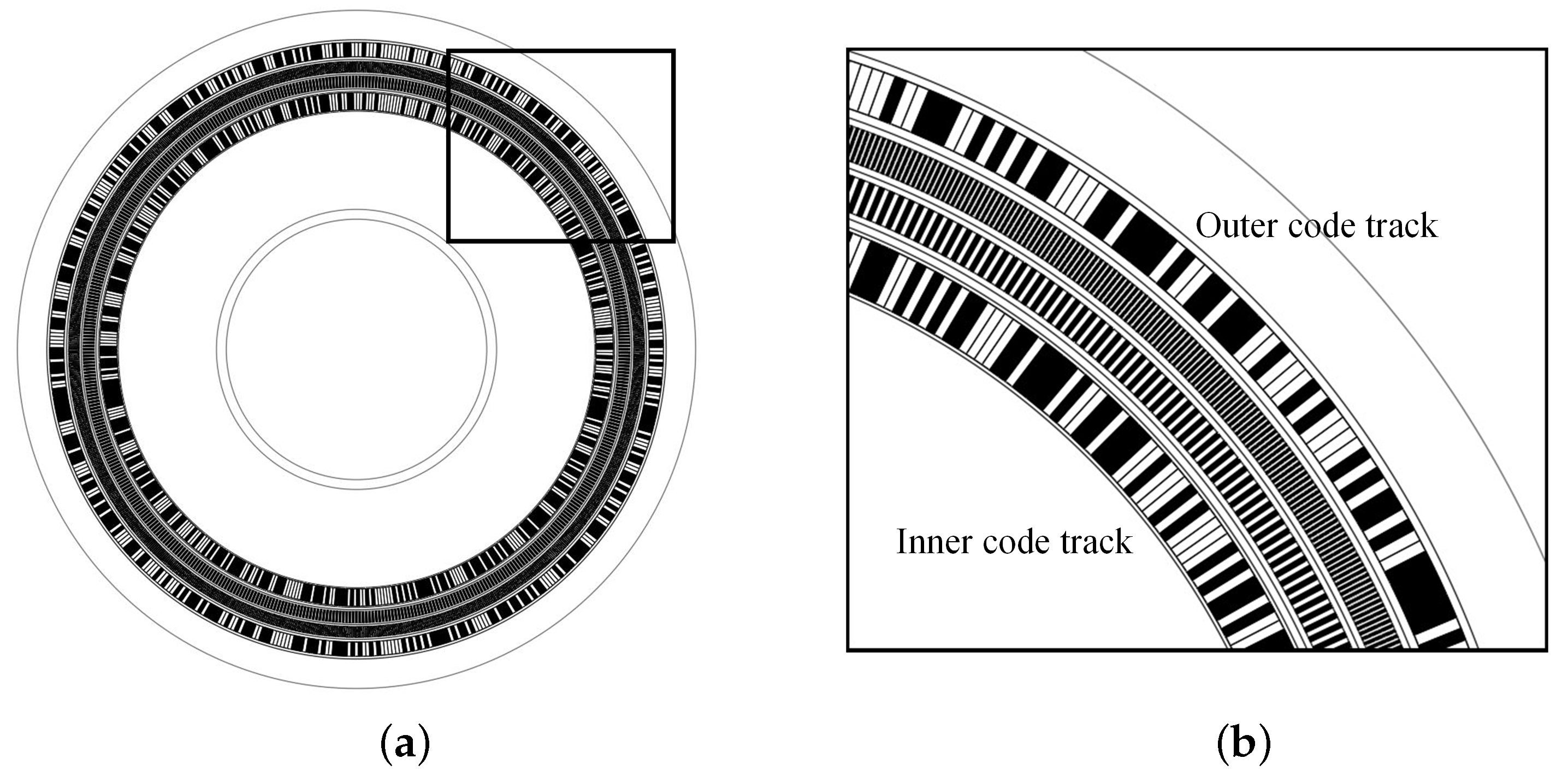
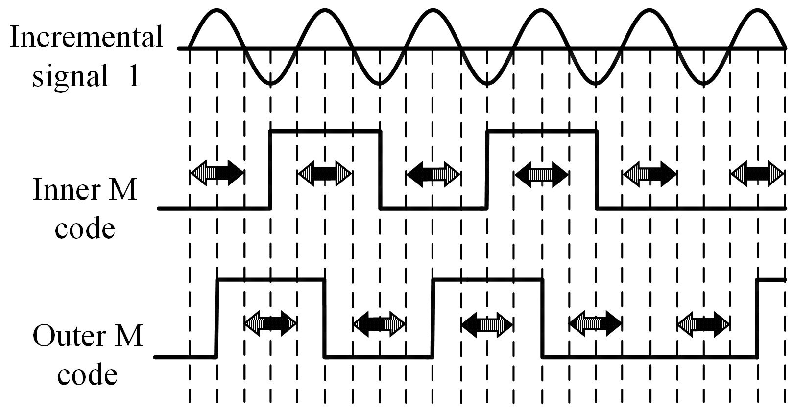
2. Principle of Reflective Hybrid Optical Encoder

The reflective optical encoder integrates a light source and photodiode arrays and is placed on one side of the optical code disk. When the code disk rotates, the light emitted by the light source is reflected by the code disk to form alternating light and dark stripes corresponding to the code disk pattern and return to the photodiode arrays. Photodiodes are illuminated by the reflected light and dark stripes and produce photocurrents corresponding to the light intensity. After the processing of the following circuit, the code disk pattern at the current position and the angle information corresponding to the pattern can be obtained.
The hybrid optical encoder’s code disk integrates both incremental code tracks and absolute code tracks. The code disk structure used in this study adopts a four-track design. As shown in Figure 1, the innermost and outermost code tracks on the code disk are absolute code tracks, and the two middle code tracks are incremental code tracks. There are 512 light and dark stripes with the same sequence on the two absolute code tracks, and the coding method is M-code [9]. M-code, also known as the maximum length sequence, is a pseudo-random sequence composed of binary digits 0/1. For an M sequence of n bits, all subsequences of length n are unique and occur only once in a cycle [22]. Therefore, the M-code can be used to encode the angle value on the circumference uniquely, and the absolute position information can be obtained by decoding.
Since the signal at the junction of the light and dark stripes is prone to miscoding when reading discrimination, the relative positions of the two M-code tracks on the code disk in the direction of rotation are designed to differ by half a bit (half the width of a code element). In this way, when the junction of the light and dark stripes of the outer M-code track rotates to the center of the outer photodiode array, the light and dark stripes generated by the inner M-code track align with the inner photodiode array. At this time, the signal of the inner photodiode array can be read to obtain the current position information and vice versa. In this way, the detection accuracy can be improved, and the bit error rate can be reduced. The selection of the two M-code track signals is realized by the sinusoidal signal generated by the incremental code track close to the inner side. There are 512 pairs of light and dark stripes on this incremental code track, and the width of a pair of light and dark stripes corresponds to the width of one stripe in the M-code track. During the rotation process, the period of the sinusoidal signal generated by the incremental code track is the same as the period of one code element of the absolute code. During the 0°~180° period of one sinusoidal signal, the signal of the inner M-code track is read, and during the 180°~360° period, the signal of the outer M-code track is read, so as to achieve the selection of the M-code track signals, as shown in Figure 2. The black arrows in Figure 2 mark the reading range of the two M-code track signals. There are 1024 pairs of light and dark stripes on the incremental code track near the outer side, which are used to achieve angle subdivision.

3. Theoretical Analysis of Light Intensity and Compensation Design

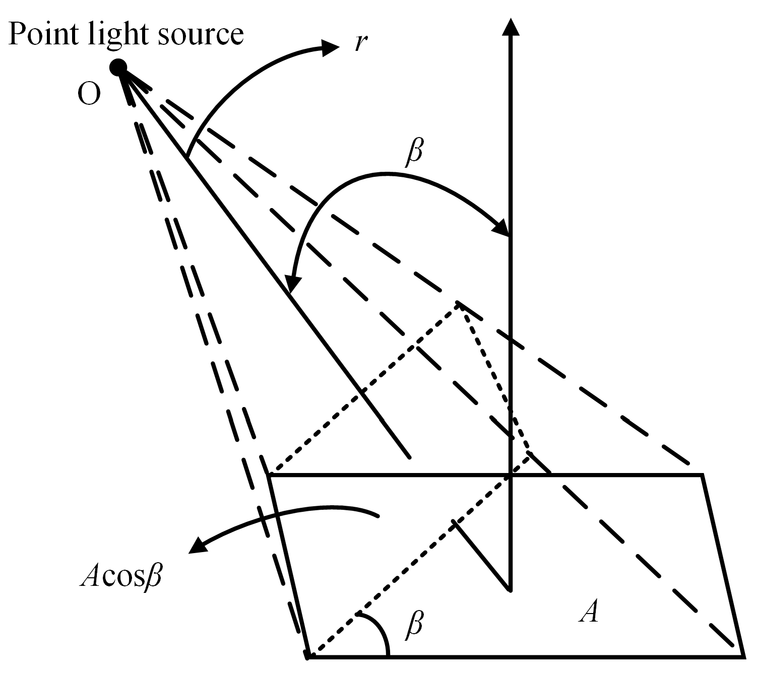
3.1. Analysis of LED Luminous Characteristics

In the ideal case, a single LED light source can be approximately regarded as a Lambertian light source, and the expression of its light intensity distribution is as follows:
I ( θ ) = I 0 cos m θ
where θ is the luminous angle, and I 0 is the light intensity of the LED along the normal direction of the light source surface ( θ = 0 ). The value of m is related to the half-light intensity angle θ 1 / 2 of the LED, and their relationship is as follows:
m = ln 2 ln cos θ 1 / 2
where θ 1 / 2 is defined as the angle of luminescence when the luminous intensity is reduced to half of the light intensity in the normal direction. The light source used in this study is a GaAs-based LED chip, whose luminous band is 845~855 nm, and its half-intensity angle θ 1 / 2 is 62.4°. According to Equation (2), we can calculate m = 0.9009 .
When the light source vertically irradiates the receiving surface, the illumination degree of the receiving surface can be expressed by the irradiance E. The relationship between irradiance E, luminous intensity I, and receiving surface distance r is as follows:
E = I r 2
This is the inverse square law of distance. However, when the receiving plane is not perpendicular to the direction of light irradiation, as shown in Figure 3, the inverse square law is modified as shown in Equation (4):
E = I cos β r 2
where I is the luminous intensity in the direction of the receiving surface. β is the angle between the light irradiation direction and the normal line of the receiving surface, and r is the distance between the light source and the receiving surface.
Substituting Equation (1) into Equation (4), the irradiance E θ received by the receiving surface at the distance from the light source r can be obtained as follows:
E θ = I θ cos β r 2 = I 0 cos m θ cos β r 2
where I 0 is the light intensity of the LED along the normal direction of the light source surface. θ is the angle between the light irradiation direction and the normal direction of the light source surface. β is the angle between the light irradiation direction and the normal line of the receiving surface. The value of m is 0.9009.

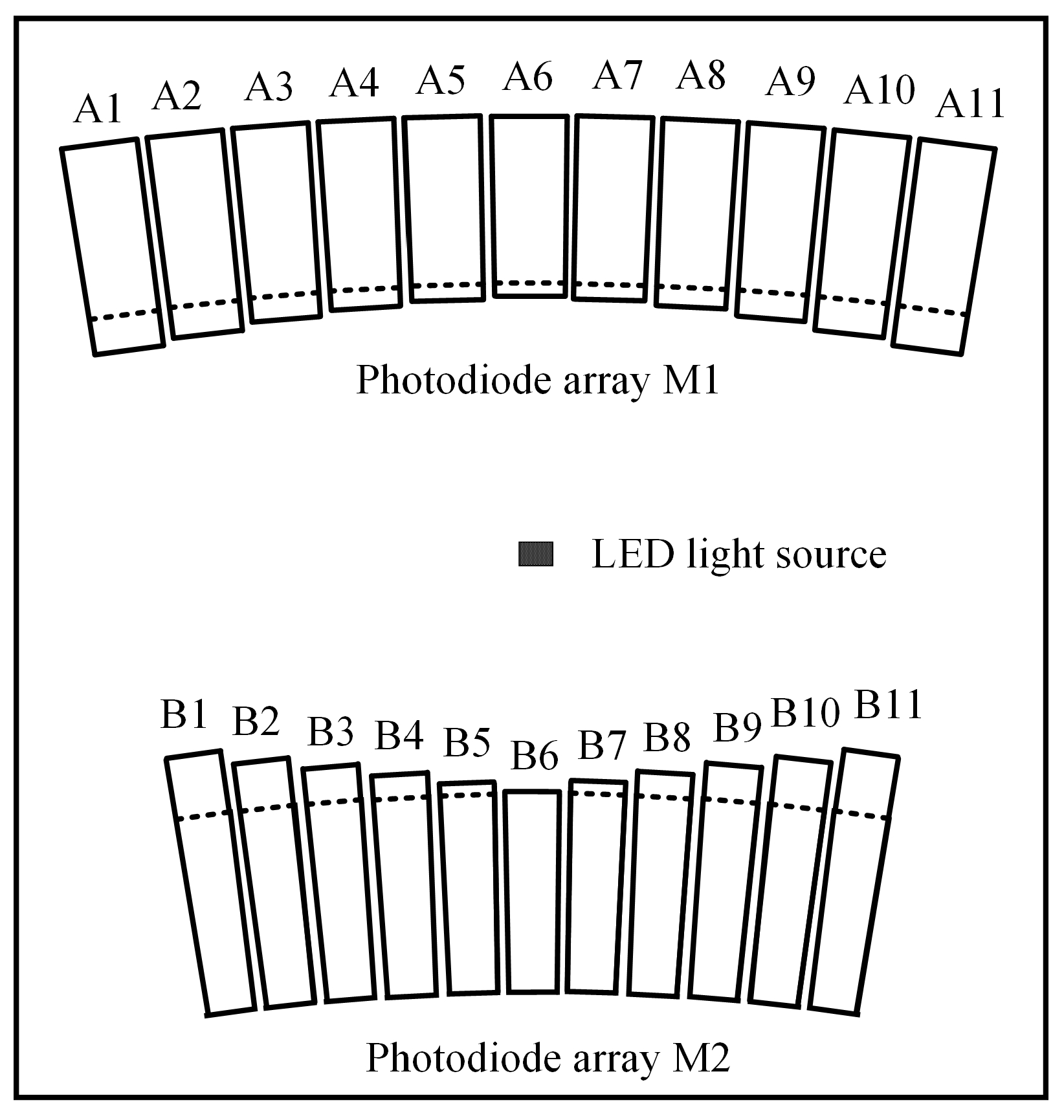
3.2. Design of Photodiode Area Compensation

The image obtained by the light source irradiating the code disk can be regarded as the image of the code track pattern magnified by ε times, as shown in Figure 4. The value of magnification ε is related to the height h from the light source to the code disk and the height H from the code disk to the photodiode arrays. According to the principle of similar triangles, the expression of magnification ε can be obtained as follows:
ε = H + h h = 2 H Δ h H Δ h
where Δ h is the height of the LED light source relative to the photodiode arrays. The imaging size and position corresponding to the code elements can be calculated according to the magnification and the pattern size of the M-code track.
After obtaining the imaging information of the code element, the photodiode can be placed at the imaging location. For the M-code track with 512 2 9 light and dark stripes, nine photodiodes are generally required. Due to the need for error detection and correction in the digital part, a redundant photodiode is added on the left and right sides so that each M-code track corresponds to 11 photodiodes, as shown by the dotted lines in Figure 5. In Figure 5, the M-code track near the outer side of the code disk corresponds to the photodiode array M1, and the M-code track near the inner side corresponds to the photodiode array M2.
In order to realize the consistency of the output signals of different channels of M-code, it is necessary to make corresponding area compensation according to the irradiance of 22 photodiodes. In this study, the photocurrent generated by the photodiode at position B6 in Figure 5 is used as the benchmark, and the area compensation is performed for the photodiodes at the remaining positions. The current I c generated by each photodiode is related to the incident light power P received by the photodiode, and their relationship is as follows:
I c = R λ × P
where R λ is the responsivity of the photodiode, which is defined as the ratio of the photocurrent generated by the photodiode to the incident light power at a certain wavelength. Its value is given by the process manufacturer, and the responsivity of the photodiodes in different positions is the same. Each photodiode’s incident light power P equals to the integral of its radiation illuminance and the light receiving area. For the convenience of calculation, Equation (5) needs to be expressed in the rectangular coordinate system. Because the light source and the photodiode arrays are in the same plane, that is, the normal of the light source surface is parallel to the normal of the receiving surface, so θ = β in Equation (5). Suppose the plane where the light source is located is the x y plane, and the z-axis represents the normal direction of the LED light source surface. If the coordinates of the light source are X , Y , 0 , the expression of Equation (5) in the rectangular coordinate system is as follows:
E x , y , z = z m + 1 I 0 x X 2 + y Y 2 + z 2 m + 3 / 2
where x, y and z are the coordinates of any point on the receiving surface. I 0 is the light intensity of the LED along the normal direction of the light source surface. So the relationship between the incident light power P and the position and area of the photodiode is as follows:
P = x 1 x 2 y 1 y 2 E x , y , z d x d y = x 1 x 2 y 1 y 2 z m + 1 I 0 x X 2 + y Y 2 + z 2 m + 3 / 2 d x d y
In actual use, the height of the light source from the code disk is determined, so z in Equation (9) is a constant. According to Equations (7) and (9), the photocurrent generated by photodiode B6 can be calculated. Then, based on this current, the photodiodes in other positions are compensated with different degrees of area to make their photocurrents equal to this reference current. The specific compensation height value is calculated by MATLAB software according to Equation (9). After the compensation height is obtained, the lengths of the upper and lower sides of the new compensated photodiodes can be calculated according to the imaging principle. The shape of the photodiodes can be approximated as a trapezoid, and the new area information of the photodiodes after compensation can be calculated according to the area formula of the trapezoid. The size information of the photodiode at each position after compensation is shown in Table 1, and the schematic diagram of the photodiode arrays after compensation is shown as the solid lines in Figure 5.

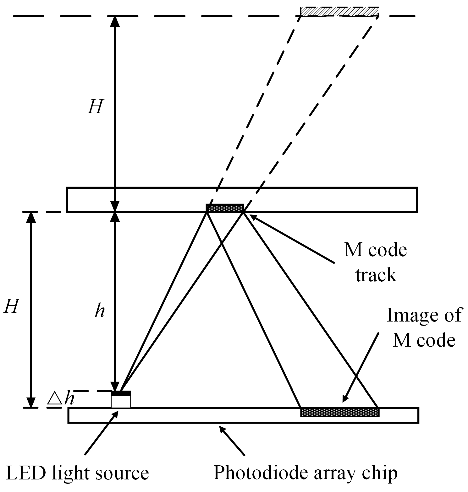
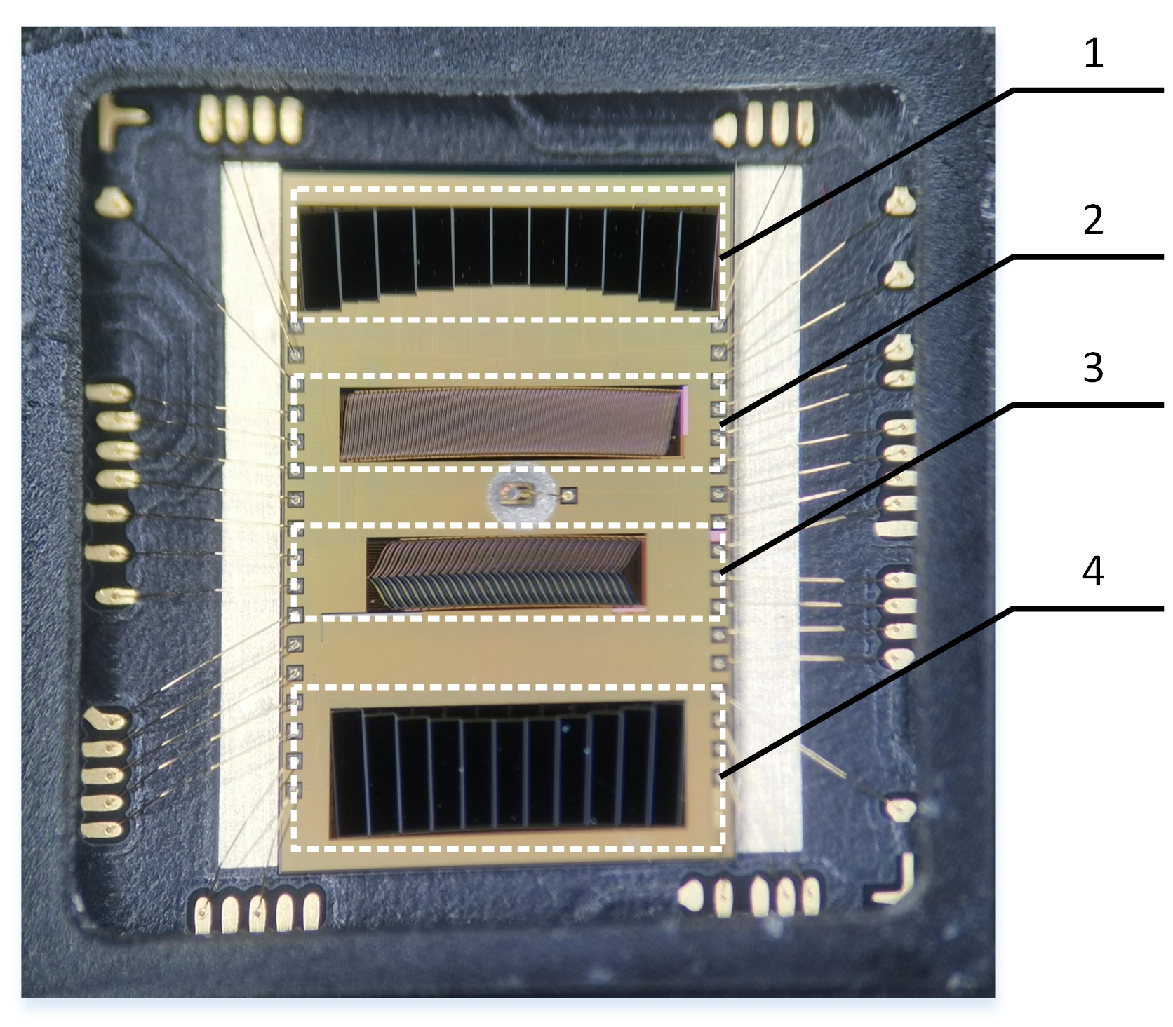
3.3. Chip Implementation

The chip has four photodiode arrays corresponding to four code tracks. Each M-code photodiode array has 11 photodiodes that read out 11-bit M-codes in parallel to provide absolute position information. The photodiodes corresponding to the two incremental codes adopt an array structure. Each incremental photodiode array is divided into four groups of photodiodes, which output four sinusoidal signals with a 90° difference. One incremental array is used to assist in the readout of the M-code, and the other incremental array is used to achieve the subdivision of the angle. The chip is designed based on the 0.35 μ m CMOS process and has been taped and packaged. The area of the chip is 5.5 mm × 3.9 mm. Figure 6 shows the physical photo of the chip, in which 1 and 4 are the photodiode arrays M1 and M2 corresponding to the M-code, respectively, and 2 is the photodiode array corresponding to the incremental code used to realize the angle subdivision. Finally, 3 is the photodiode array corresponding to the incremental code used to assist in reading the M-code signals.

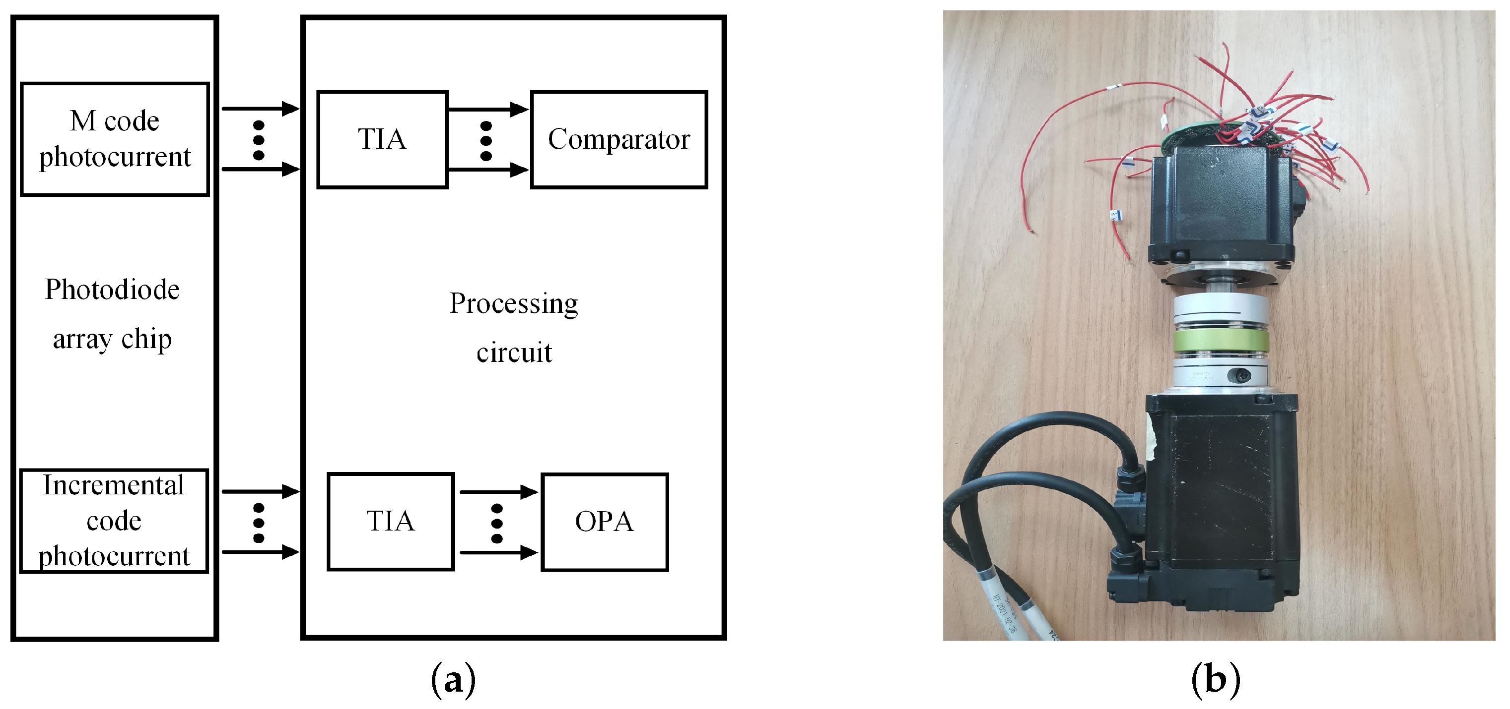
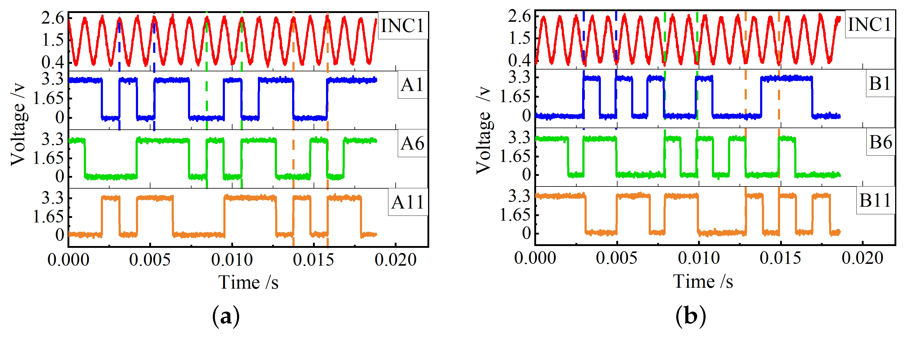
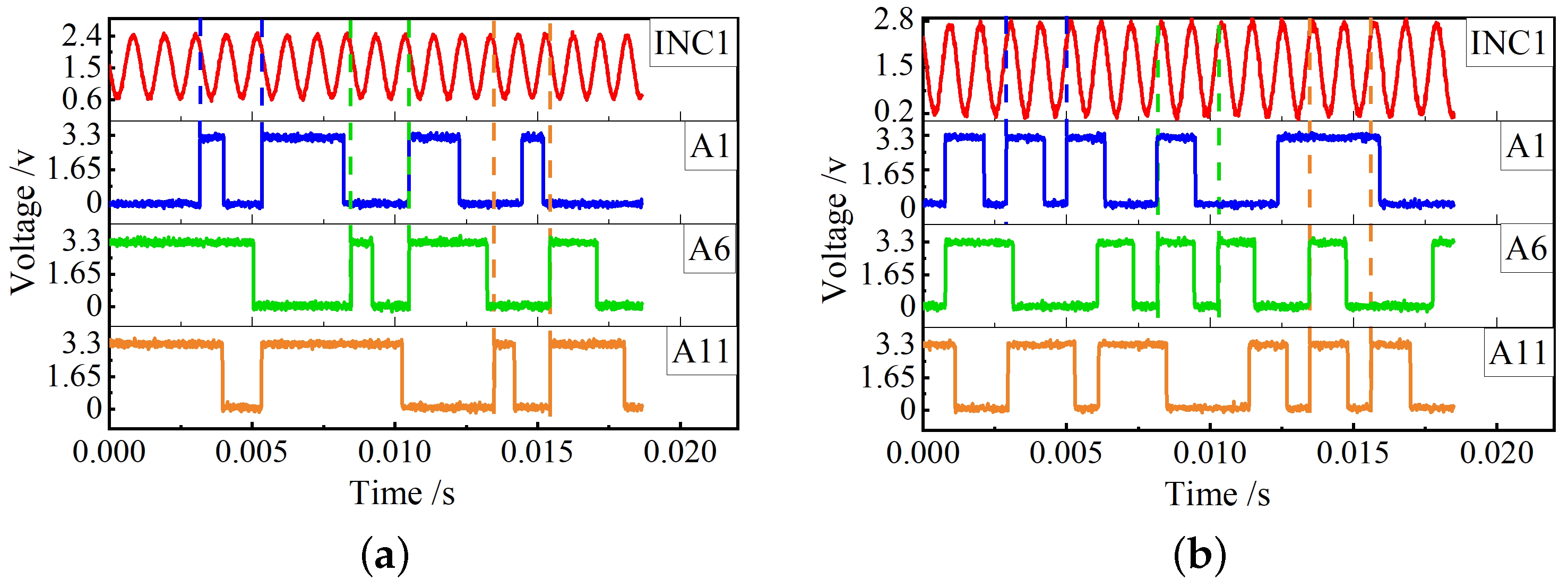
4. Testing and Analysis

In order to verify the performance of the chip, the test circuit shown in Figure 7 is built. Firstly, the photocurrents of the M-code are converted into voltages by trans-impedance amplifiers (TIA) and amplified in the first stage. Then the signals enter the comparators to be compared with the set threshold, and the analog signals are converted into digital signals corresponding to the code elements. The photocurrents of the incremental code are first converted into voltages by TIA and amplified in the first stage. Then, the operational amplifiers (OPA) convert the single-ended signals into differential signals, and secondary amplification is carried out simultaneously. The PCB, where the chip and its peripheral circuits are located, is mounted on a motor with a reflective code disk. The motor shaft drives the code disk to rotate, and the chip will generate the corresponding photoelectric signals. The generated signals are processed by the peripheral circuits and then connected to the oscilloscope. The output results are displayed by the oscilloscope.
Since the oscilloscope has only four channels, it is impossible to simultaneously test all the outputs of the M-code photodiode arrays. To illustrate the compensation effect, the outputs of the photodiodes farthest and closest to the light source in each M array are taken as an example for illustration, that is, the outputs of photodiodes A1, A6, A11 and B1, B6, B11 in Figure 5. At the same time, an oscilloscope channel is reserved for displaying the incremental signal INC1 of the auxiliary M-code readout. Ideally, the duty cycle of the square wave signal generated by a pair of light and dark stripes on the code disk is 50%. When the LED working current is 13.56 mA and the reference level of the comparators is 0.85V, the square waves of signals of channels A1, A6, A11 and B1, B6, B11 after passing through comparators are shown in Figure 8a,b. The parts marked by dotted lines in Figure 8a are the square wave signals generated by the same pair of light and dark stripes in channels A1, A6, and A11. By calculation, the duty cycles of the square wave signals in channels A1, A6, and A11 are 50.2%, 49.1%, and 49.5% respectively. Similarly, the parts marked by dotted lines in Figure 8b are the square wave signals generated by another pair of light and dark stripes in channels B1, B6, and B11. By calculation, the duty cycles of the square wave signals in channels B1, B6, and B11 are 51.8%, 50.8%, and 51% respectively. The square wave duty cycle error of the six channels is within 2%, which indicates that the output signals of photodiodes at different positions have high consistency.
Then change the working current of the LED light source, and test the consistency of the output signals of each M-code channel when the LED’s luminous intensity changes. Taking the three channels A1, A6, and A11 as an example, the working current of the LED is reduced to 10.71 mA. At this time, the luminous intensity of the LED decreases, and the photocurrents generated by the photodiode arrays decrease. When the reference level of the comparators remains unchanged, the duty cycles of the square wave signals generated by a pair of light and dark stripes on the code disk will become smaller, as shown in Figure 9a. The parts marked by dotted lines in Figure 9a are the square wave signals generated by the same pair of light and dark stripes in channels A1, A6, and A11. After calculation, the duty cycles of the square wave signals in the three channels are 38.2%, 36.5%, and 36.2% respectively. Similarly, when the working current of the LED is increased to 16.41 mA, the luminous intensity of the LED will increase, and the photocurrents generated by the photodiode arrays will increase. By keeping the reference level of the comparators unchanged, the duty cycles of the square wave signals generated by a pair of light and dark stripes on the code disk will become larger, as shown in Figure 9b. The parts marked by dotted lines in Figure 9b are the square wave signals generated by another pair of light and dark stripes in channels A1, A6, and A11. After calculation, the duty cycles of the square wave signals in the three channels are 63.3%, 60.2%, and 61.7% respectively. It can be seen that when the LED working current changes by ±2.85 mA, the square wave duty cycle error of the three channels is within 3.1%. Therefore, even if the LED’s luminous intensity changes, the M-code channels’ output signals still have good consistency.
At the same time, the phase relationship between M-code photodiode arrays M1 and M2 is verified. Taking A6 and B6 closest to the light source and A11 and B11 farthest from the light source as examples, the test results are shown in Figure 10. It can be seen from the dotted lines in Figure 10 that the phase difference between the output signals of A6 and B6 channels is half the period of the incremental signal INC1, and the phase difference between the output signals of A11 and B11 channels is also half the period of the incremental signal INC1. This is consistent with the previous theoretical analysis, and the phase relationship of the photodiode arrays M1 and M2 meets the design requirements.

5. Conclusions

This paper proposes a photodiode area-compensation method applied to an optical encoder chip. This method compensates the area of the photodiode arrays of the M-code according to the light intensity distribution characteristics of the light source to achieve a high consistency of the output signals of the M-code. Using this method, a photodiode array chip for a reflective hybrid optical encoder is designed based on the 0.35 μ m CMOS process. When the LED is working normally, the duty cycle error of the square wave signals output by the M-code is within 2%, and even when the LED light intensity changes, the duty cycle error of the square wave signals output by the M-code is within 3.1%. The experimental results show that the output signals of each channel of the M-code have high consistency. Therefore, the same readout circuit can be used for each channel of M-code, which greatly simplifies the design complexity of the processing circuit. Moreover, when the LED luminous intensity changes due to temperature, aging, and other reasons, it is relatively simple to adjust and not easy to generate error codes. Although the area compensation method has high requirements for the calculation of light intensity distribution and the accuracy of chip installation, it is a relatively simple method to achieve the consistency of output signals and reduce the bit error rate. This method has certain reference significance for applying reflective hybrid optical encoders practically.

Author Contributions

Conceptualization, X.W. and Y.L.; methodology, X.W. and W.Z.; software, X.W. and X.Y.; validation, X.W. and D.H.; data curation, X.Y.; formal analysis, X.W.; funding acquisition, W.Z.; investigation, X.W.; project administration, Y.L.; resources, X.W. and Y.L.; supervision, Y.L.; visualization, X.W.; writing—original draft preparation, X.W.; writing—review and editing, W.Z. All authors have read and agreed to the published version of the manuscript.

Funding

This research received no external funding.

Data Availability Statement

Not applicable.

Conflicts of Interest

The authors declare no conflict of interest.

References

  1. Rodriguez-Donate, C.; Osornio-Rios, R.A.; Rivera-Guillen, J.R.; de Jesus Romero-Troncoso, R. Fused smart sensor network for multi-axis forward kinematics estimation in industrial robots. Sensors 2011, 11, 4335–4357. [Google Scholar] [CrossRef] [PubMed] [Green Version]
  2. Tameh, T.A.; Sawan, M.; Kashyap, R. Novel analog ratio-metric optical rotary encoder for avionic applications. IEEE Sens. J. 2016, 16, 6586–6595. [Google Scholar] [CrossRef]
  3. Fleming, W.J. Overview of automotive sensors. IEEE Sens. J. 2001, 1, 296–308. [Google Scholar] [CrossRef] [Green Version]
  4. Song, J.H.; Kim, K.C.; Kim, S.H. Reducing tilt errors in moiré linear encoders using phase-modulated grating. Rev. Sci. Instrum. 2000, 71, 2296–2300. [Google Scholar] [CrossRef] [Green Version]
  5. Ye, G.; Liu, H.; Ban, Y.; Shi, Y.; Yin, L.; Lu, B. Development of a reflective optical encoder with submicron accuracy. Opt. Commun. 2018, 411, 126–132. [Google Scholar] [CrossRef]
  6. Johnson, N.; Mohan, K.J.; Janson, K.E.; Jose, J. Optimization of incremental optical encoder pulse processing. In Proceedings of the 2013 International Mutli-Conference on Automation, Computing, Communication, Control and Compressed Sensing (iMac4s), Kottayam, India, 22–23 March 2013; pp. 769–773. [Google Scholar]
  7. Petriu, E. Absolute position measurement using pseudo-random binary encoding. IEEE Instrum. Meas. Mag. 1998, 1, 19–23. [Google Scholar] [CrossRef] [Green Version]
  8. Kim, J.A.; Kim, J.W.; Kang, C.S.; Jin, J.; Bong Eom, T. An optical absolute position measurement method using a phase-encoded single track binary code. Rev. Sci. Instrum. 2012, 83, 115115. [Google Scholar] [CrossRef] [PubMed]
  9. Matsuzoe, Y.; Tsuji, N.; Nakayama, T.; Fujita, K.; Yoshizawa, T. High-performance absolute rotary encoder using multitrack and M-code. Opt. Eng. 2003, 42, 124–131. [Google Scholar] [CrossRef]
  10. Liu, H.; Ye, G.; Shi, Y.; Yin, L.; Chen, B.; Lu, B. Multiple harmonics suppression for optical encoders based on generalized grating imaging. J. Mod. Opt. 2016, 63, 1564–1572. [Google Scholar] [CrossRef]
  11. Mitchell, D.K. A radiation-hardened, high-resolution optical encoder for use in aerospace applications. In Proceedings of the 2008 IEEE Aerospace Conference, Big Sky, MT, USA, 1–8 March 2008; pp. 1–7. [Google Scholar]
  12. Rozman, J.; Pletersek, A. Linear Optical Encoder System with Sinusoidal Signal Distortion Below −60 dB. IEEE Trans. Instrum. Meas. 2009, 59, 1544–1549. [Google Scholar] [CrossRef]
  13. Ye, G.; Liu, H.; Shi, Y.; Yin, L.; Lu, B.; Hui, X.; Yang, Y. Optimizing design of an optical encoder based on generalized grating imaging. Meas. Sci. Technol. 2016, 27, 115005. [Google Scholar] [CrossRef]
  14. Ye, G.; Liu, H.; Jiang, W.; Li, X.; Jiang, W.; Yu, H.; Shi, Y.; Yin, L.; Lu, B. Design and development of an optical encoder with sub-micron accuracy using a multiple-tracks analyser grating. Rev. Sci. Instrum. 2017, 88, 015003. [Google Scholar] [CrossRef] [PubMed]
  15. Yu, H.; Wan, Q.; Zhao, C.; Han, Q.; Mu, Z. Error compensation for low-density circular gratings based on linear image-type angular displacement measurements. IEEE Trans. Ind. Electron. 2022, 69, 13736–13743. [Google Scholar] [CrossRef]
  16. Xiao, K.; Wang, L. Analysis and error compensation of electric sine/cosine encoder. In Proceedings of the 2009 9th International Conference on Electronic Measurement & Instruments, Beijing, China, 16–19 August 2009; pp. 1–87. [Google Scholar]
  17. Ye, G.; Xing, H.; Liu, H.; Li, Y.; Lei, B.; Niu, D.; Li, X.; Lu, B.; Liu, H. Total error compensation of non-ideal signal parameters for Moiré encoders. Sens. Actuator A Phys. 2019, 298, 111539. [Google Scholar] [CrossRef]
  18. Gottardi, M.; Gonzo, L.; Gregori, S.; Liberali, V.; Simoni, A.; Torelli, G. An integrated CMOS front-end for optical absolute rotary encoders. Analog Integr. Circuits Process. 2003, 34, 143–154. [Google Scholar] [CrossRef]
  19. Maschera, D.; Simoni, A.; Gottardi, M.; Gonzo, L.; Gregori, S.; Liberali, V.; Torelli, G. An automatically compensated readout channel for rotary encoder systems. IEEE Trans. Instrum. Meas. 2001, 50, 1801–1807. [Google Scholar] [CrossRef]
  20. Seybold, J.; Bülau, A.; Fritz, K.P.; Frank, A.; Scherjon, C.; Burghartz, J.; Zimmermann, A. Miniaturized optical encoder with micro structured encoder disc. Appl. Sci. 2019, 9, 452. [Google Scholar] [CrossRef] [Green Version]
  21. Liberali, V.; Cherchi, F.; Disingrini, L.; Gottardi, M.; Gregori, S.; Torelli, G. A digital self-calibration circuit for absolute optical rotary encoder microsystems. IEEE Trans. Instrum. Meas. 2003, 52, 149–157. [Google Scholar] [CrossRef]
  22. Yan, Y.J.; Liao, C.C.; Wang, T.F.; Ou-Yang, M. Optimizing the De-Bruijn code of rotary optical encoders preventing from the photocurrent blooming. IEEE Sens. J. 2020, 21, 1493–1503. [Google Scholar] [CrossRef]
Figure 1. (a) Overall code disk structure. (b) Local code disk structure.
Electronics 11 03997 g001
Figure 2. Reading relationship between incremental signal and M-code signal.
Electronics 11 03997 g002
Figure 3. Solid angle relationship when the receiving plane is not perpendicular to the light direction.
Electronics 11 03997 g003
Figure 4. Schematic diagram of code track pattern amplification relationship.
Electronics 11 03997 g004
Figure 5. Photodiode arrays corresponding to M-code track.
Electronics 11 03997 g005
Figure 6. Photo of chip.
Electronics 11 03997 g006
Figure 7. (a) Schematic diagram of test circuit. (b) Photo of test system.
Electronics 11 03997 g007
Figure 8. (a) Signals of A1, A6 and A11 channels of M-code after TIA and comparator processing. (b) Signals of B1, B6 and B11 channels of M-code after TIA and comparator processing.
Electronics 11 03997 g008
Figure 9. (a) Signals output by A1, A6 and A11 channels when LED luminous intensity decreases. (b) Signals output by A1, A6 and A11 channels when LED luminous intensity increases.
Electronics 11 03997 g009
Figure 10. (a) Phase relationship of A6 and B6 output signals. (b) Phase relationship of A11 and B11 output signals.
Electronics 11 03997 g010
Table 1. Size information of photodiodes at each position of M arrays after area compensation.
PhotodiodeHeight (µm)Top Length (µm)Bottom Length (µm)Photodiode Area (µm 2 )
A1/A11810.9478303.9871313.4860250,369.2260
A2/A10734.4633304.8830313.4860227,084.6682
A3/A9677.2732305.5529313.4860209,629.2284
A4/A8637.6607306.0169313.4860197,516.3264
A5/A7614.3909306.2895313.4860190,392.2136
A6606.7166306.3794313.4860188,041.3140
B1/B111032.7972248.1883260.1652262,513.0357
B2/B10959.8140248.1883259.3189243,556.2578
B3/B9904.8245248.1883258.6812229,313.9710
B4/B8866.4818248.1883258.2365219,403.9361
B5/B7843.8465248.1883257.9740213,561.6426
B6836.3628248.1883257.8872211,631.3611
Publisher’s Note: MDPI stays neutral with regard to jurisdictional claims in published maps and institutional affiliations.

