Article

Design of a Quadruple Band-Notched Ultra-Wideband (UWB) Antenna Using Curled C-Shaped Structures and Interdigital Inductance Slots

1
School of Electronic Engineering, Beijing University of Posts and Telecommunications, Haidian District, Beijing 100876, China
2
The School of Automation, Beijing University of Posts and Telecommunications, Haidian District, Beijing 100876, China
*
Author to whom correspondence should be addressed.
Electronics 2022, 11(23), 3949; https://doi.org/10.3390/electronics11233949
Submission received: 21 October 2022 / Revised: 14 November 2022 / Accepted: 26 November 2022 / Published: 29 November 2022

Abstract

:
In this paper, a novel ultra-wideband (UWB) printed antenna with quadruple band-notched characteristics is proposed and investigated. The quadruple band rejections are achieved by etching two interdigital capacitance slots on each side of the ground plane, embedding a curled C-shaped slot on the circle patch, and adding a curled split-ring resonator on the backside of the antenna. Interdigital inductance slots can obtain a narrower notched band than general structures due to their high inductance, thereby preserving some valuable frequencies. Adjusting the tail branch’s length and distance of the curled C-shaped slot and the curled split-ring resonator can control the notch frequency and width. Finally, the proposed antenna operates from 2.9–11 GHz (VSWR < 2) with four band stops (VSWR > 2) for rejecting WiMAX, WLAN, and downlink of X-band satellite communication. Furthermore, the difference between the experimental results and the expected value is less than 3%. The proposed antenna can accurately filter out narrow-band signals.

1. Introduction

The research on broadband antennas in industry and academia is ongoing. Vivaldi antennas, dielectric resonant antennas, and planar antennas can provide a wide bandwidth [1,2,3,4,5,6]. Since the Federal Communications Commission (FCC) allocated the frequency band from 3.1 GHz to 10.6 GHz for commercial UWB systems, UWB printed antennas have been endowed with the ability to be used in short-range, high-speed communication systems [7]. However, UWB antennas are also highly susceptible to in-band interference, for instance, WiMAX (IEEE 802.16) systems operating at 3.3–3.7 GHz, wireless local area networks (WLANs) operating at 5.15–5.35 GHz and 5.725–5.825 GHz, and downlink of X-band satellite communication operating at 7.25–7.75 GHz [8]. The general method is to filter out the interfering frequency bands by cascading UWB antennas with filters. However, the use of filters increases the complexity and cost of UWB systems, as well as causes electromagnetic interference between components. Using an antenna with band-notched characteristics is one of the simple, effective, and low-cost filter methods. Many structures have been developed to achieve band-notched antennas, such as etching Ω-shaped, L-shaped, and U-shaped slots on the antenna radiating element and ground [9,10,11,12,13,14]. Adding parasitic structures is another way to create band rejections, such as loading split-ring resonators (SRR), U-shaped resonators, or fork-shaped structures on the back of the antenna [15,16,17,18]. Due to the wide notch bandwidth of the general band-notched structures, it is difficult to accurately filter out the narrow-band frequencies, resulting in a waste of useful frequency bands. Therefore, further research on structures with narrow-band filtering properties is required.
This paper proposes a quadruple band-notched UWB antenna using cured C-shaped structures and interdigital inductance slots, which have narrow-band filtering properties. The front of the antenna consists of a circular patch antenna and a side-feed microstrip line. Band stops of WLAN are achieved by etching two interdigital inductance slots on the ground plane. At the same time, curled C-shaped slots are etched on the radiation patch on the front of the antenna, and a curled split-ring resonator is used on the backside of the antenna to realize the band stops of WiMAX and downlink of the X-band satellite communication.

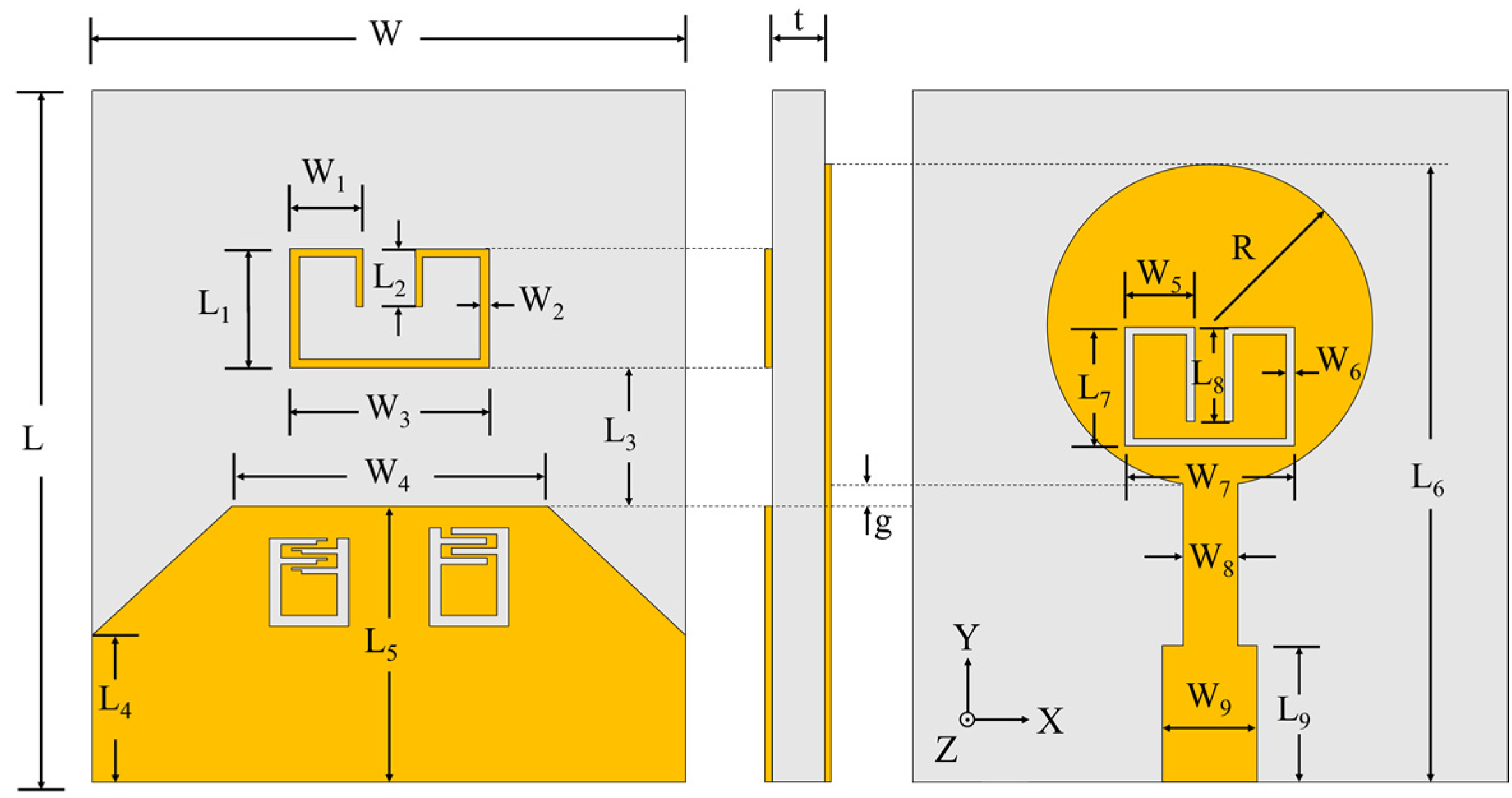
2. Proposed UWB Antenna with Quadruple Band Rejections

The geometry of the UWB monopole antenna is shown in Figure 1. The antenna is fabricated on a Rogers RT/duroid5880 substrate with a relative permittivity of 2.2, and the loss tangent is 0.0009. The overall size of the antenna is 30 mm × 35 mm × 1.575 mm. The radiator and a feed line are printed on the front side of the substrate, and the ground plane is printed on the backside of the substrate. A quarter wavelength converter is connected in series at the end of the feeder to realize the characteristic impedance matching of 50 Ω. Due to the antenna’s gradual change structure, it can match over a wide frequency range.

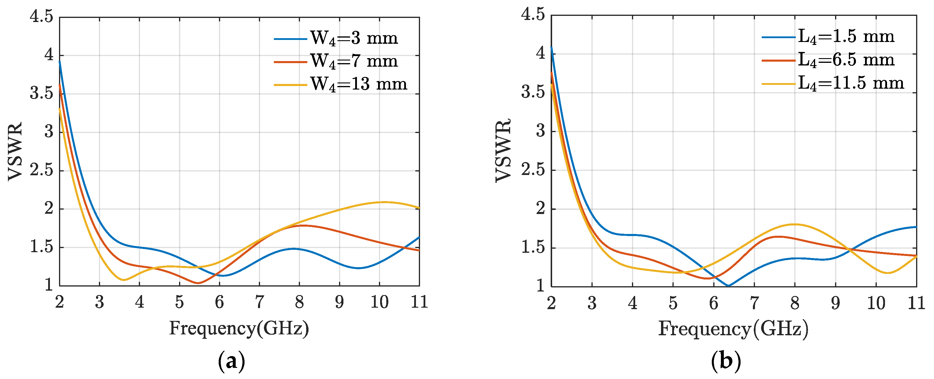
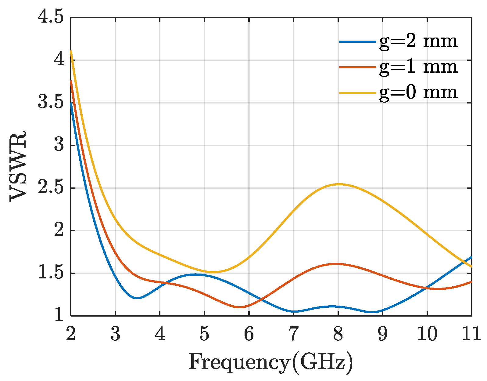
2.1. Antenna Frequency Broadening

The antenna and the ground can be equivalent to a dipole antenna [19]. Making the appropriate size cutouts on both ends of the ground plane can affect the electromagnetic coupling between the circular patch and the ground plane, greatly enhancing the impedance bandwidth [20]. W4 and L4 of the ground corner cut are analyzed in Figure 2. When W4 and L4 are larger, the low-frequency performance of the antenna is better. When W4 = 13 mm, the VSWR of the antenna at 9 GHz exceeds 2, and the UWB function cannot be realized. When L4 = 11.5 mm, the VSWR of the antenna oscillates in the high-frequency band. The distance between the radiating patch and the ground plane is marked as g, which is an essential factor affecting the impedance bandwidth of the antenna. Figure 3 shows the frequency characteristic curve of the VSWR of the antenna as a function of the parameter g. When g is changed from 0 mm to 2 mm, the bandwidth of the antenna displays a widening trend. When g = 0 mm, the VSWR of the antenna cannot meet the requirements of UWB. When g = 1 mm and g = 2 mm, the antennas are well matched in the UWB band. This result only corresponds to the numerical change of g, while the other size parameters of the antenna remain unchanged.

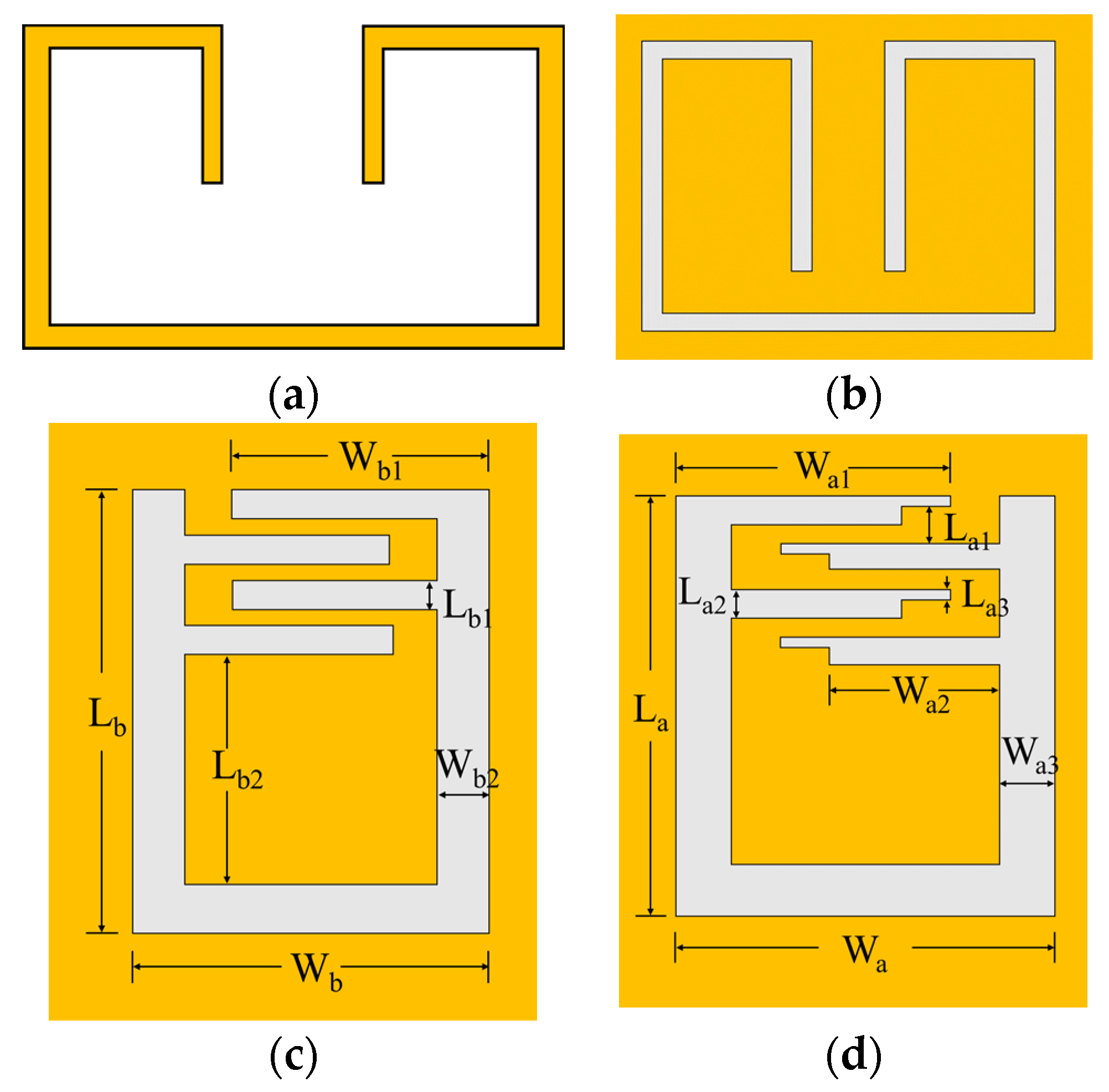
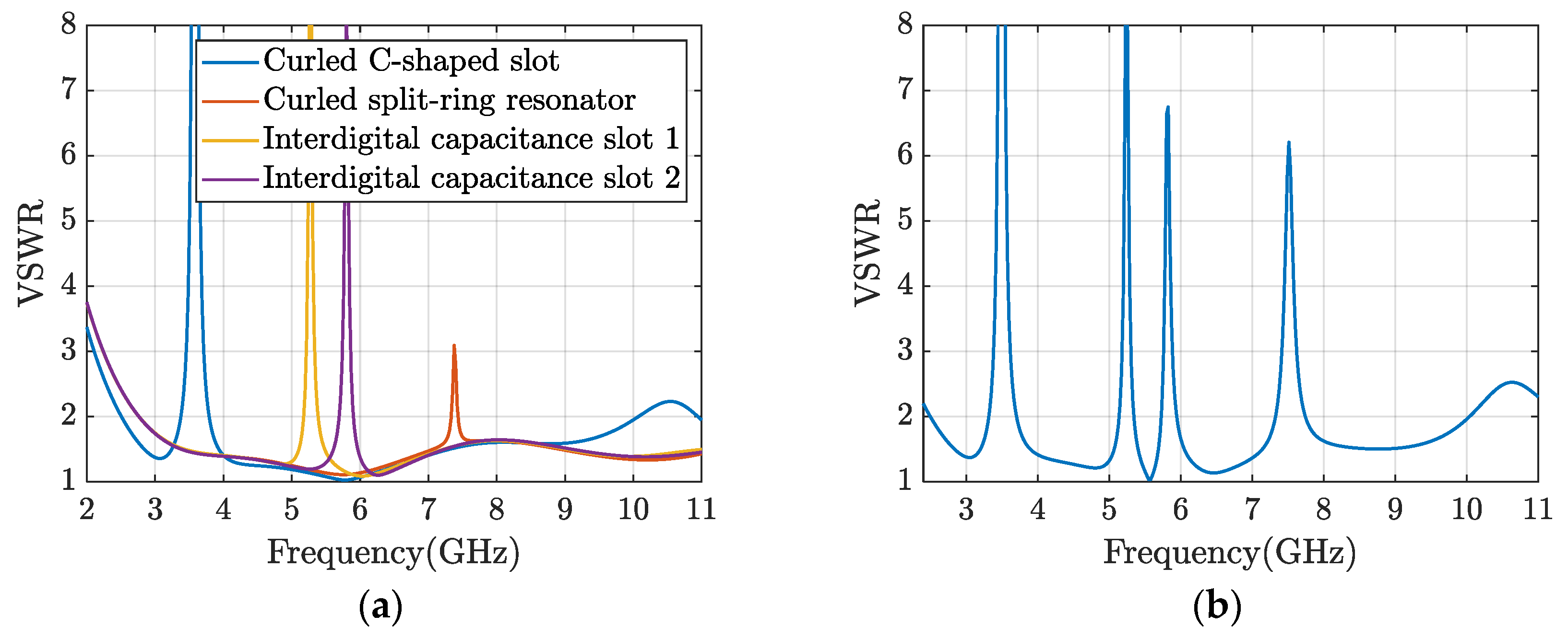
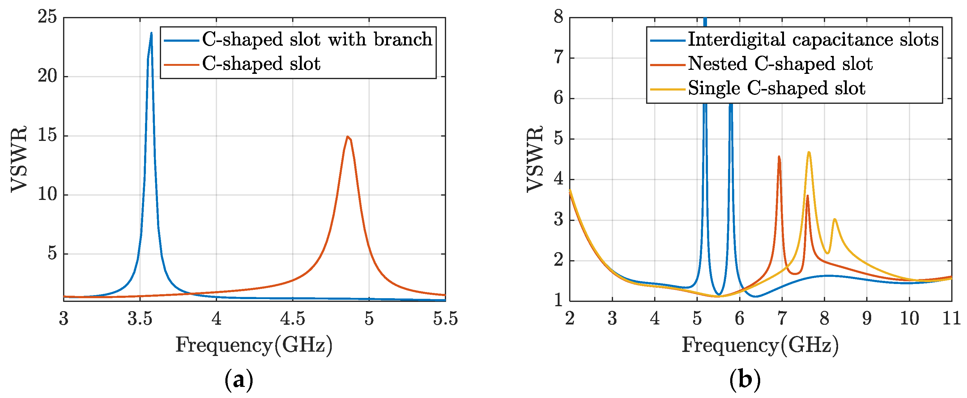
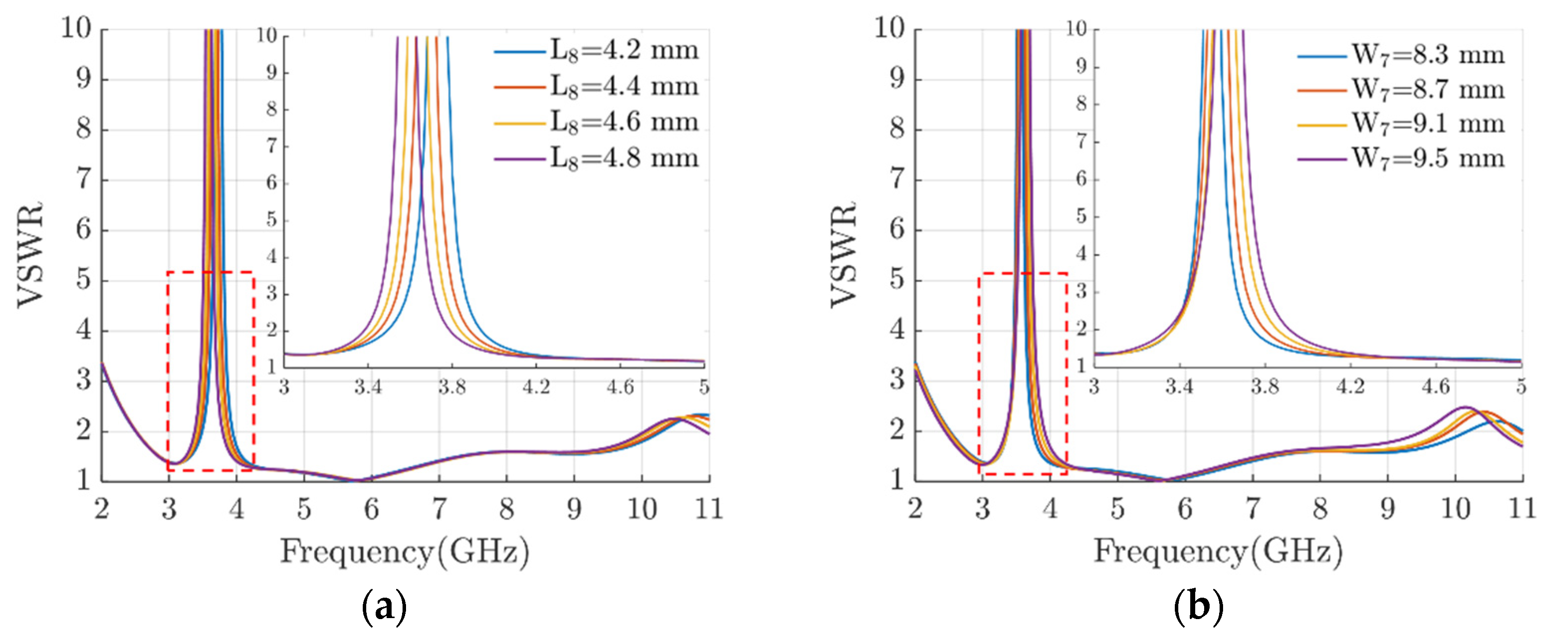
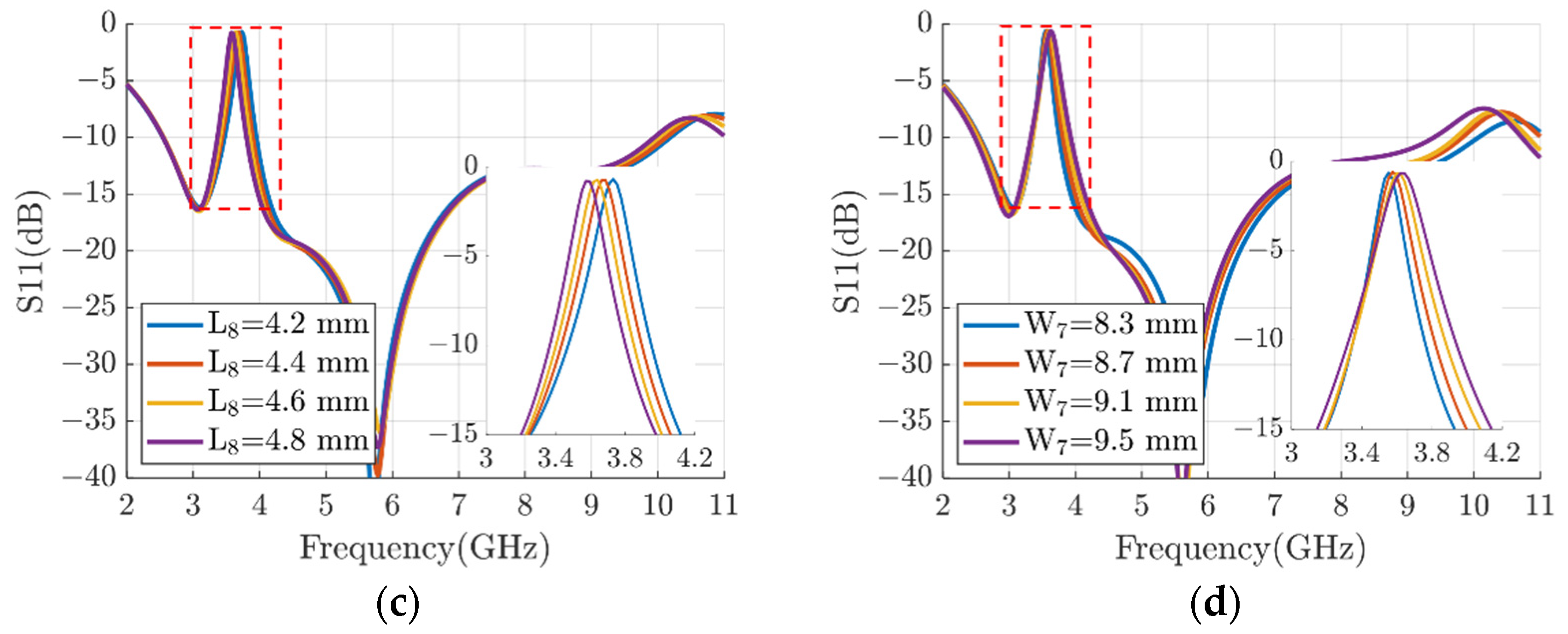
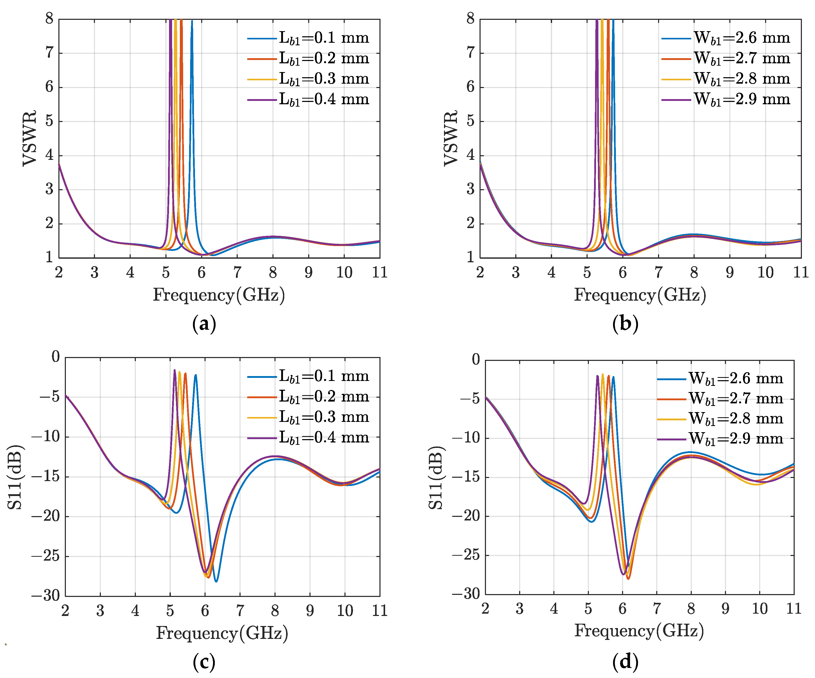
2.2. Design of Band-Notched Structures

As shown in Figure 4, four independent band-stop structures are used to achieve quadruple rejections. The required four notches are divided into two categories. One is WLAN bands with narrow notch width requirements, which are realized by etching interdigital inductance slots on the ground. The interdigital inductance slots can be regarded as improved C-shaped slots. The structure of the interdigital inductance slot consists of two parts: a C-shaped slot and an interdigitated structure. The required resonant frequency band can be achieved by a reasonable size design. Signals can be restrained in a narrow band around their resonant frequency. As the interdigital structure increases the equivalent inductance and has a higher quality factor (Q value) than the general C-slot, it can achieve a narrower resonant bandwidth [21]. The frequency f 0 of the interdigital inductance slots is 1 / 2 π L 0 C 0 . For a parallel resonant circuit, the width of the band-gap is proportional to L 0 / C 0 , where L 0 and C 0 stand for the equivalent inductance and capacitance of the interdigital inductance slots [22].
The other category is frequency bands with a wider notch width. A split-ring resonator and a C-shaped slot are used, and their length is one-half of the wavelength corresponding to the center frequency of the WiMAX and the downlinks of X-band satellite communication. The following formula can calculate the key parameters of the structures:
l e l e m e n t = λ g 2 = λ 0 2 ε r e f f = c 2 f n o t c h ε r e f f
ε r e f f = ε r + 1 2 + ε r 1 2 ( 1 + 12 h ω f ) 0.5
λ 0 is the wavelength of free space, c is the speed of light, f n o t c h is the center frequency of the notched band, ε r e f f is the effective permittivity, ε r denotes dielectric constant of the substrate, h denotes the height of the substrate, and ω f denotes the width of the feed line.
An inwardly curved extension branch is added to the tail of the general C-shaped slot and split ring resonator to increase the degree of freedom of design. By adjusting the branch’s electrical length and distance, the band-stop width’s center frequency and width can be changed.
As shown in Figure 5, the curled C-shaped slot is directly etched on the circular antenna itself, which changes the antenna structure and affects the impedance bandwidth of the antenna. It is worth noting that the structures formed by slots can realize the band notched of the antenna alone, while curled split-ring resonator cannot realize the band rejects by itself well. However, its band-stop capabilities are greatly improved when it interacts with other slots etched on the patch and ground, according to Figure 5a,b.

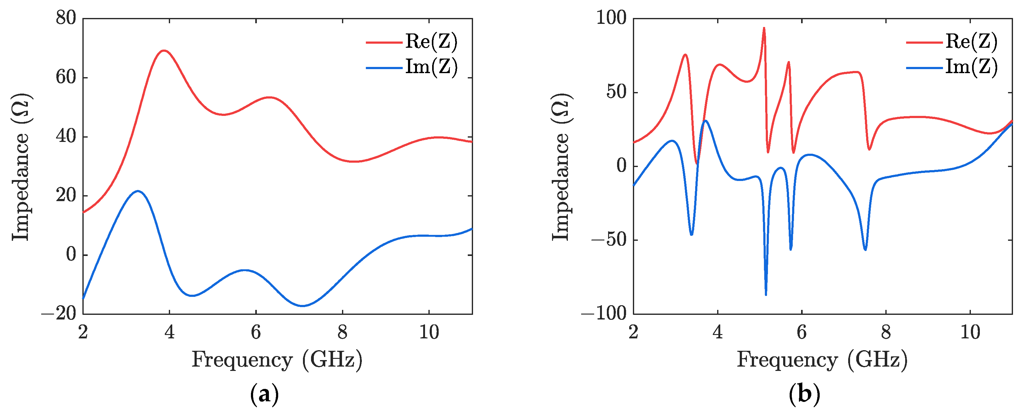
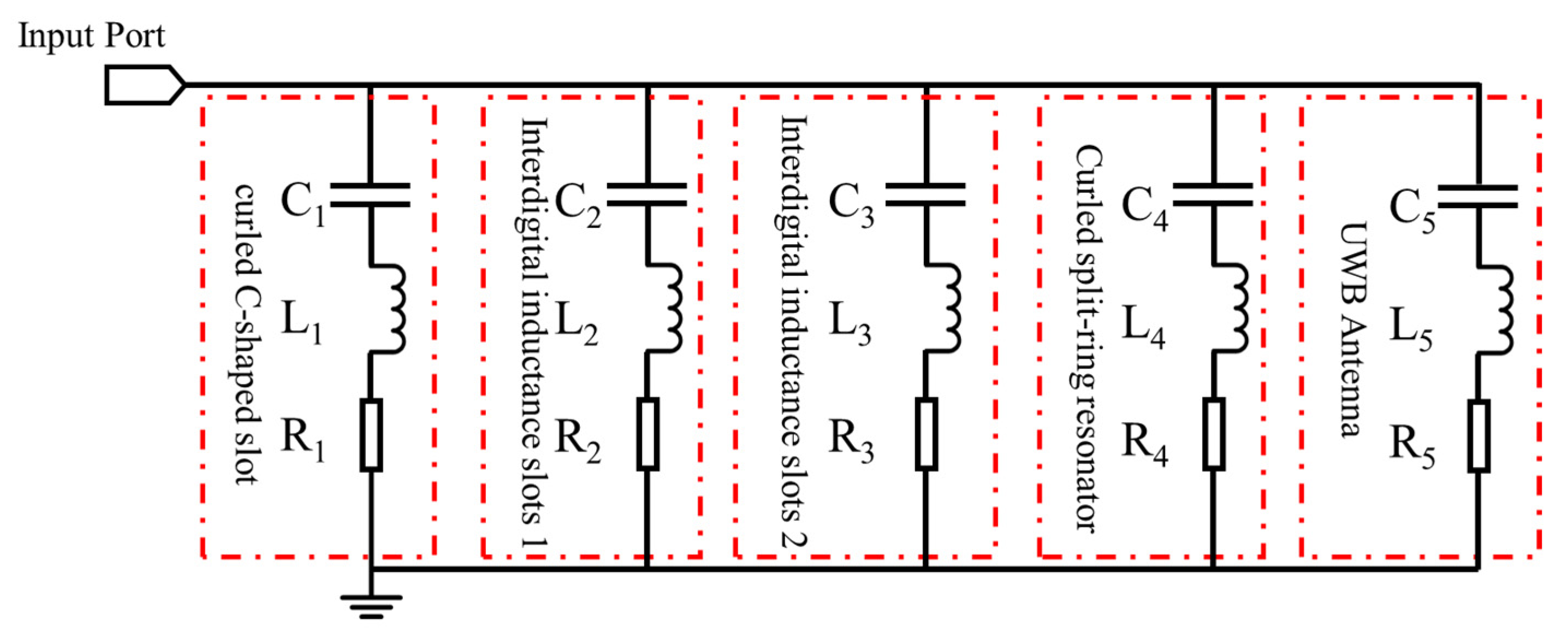
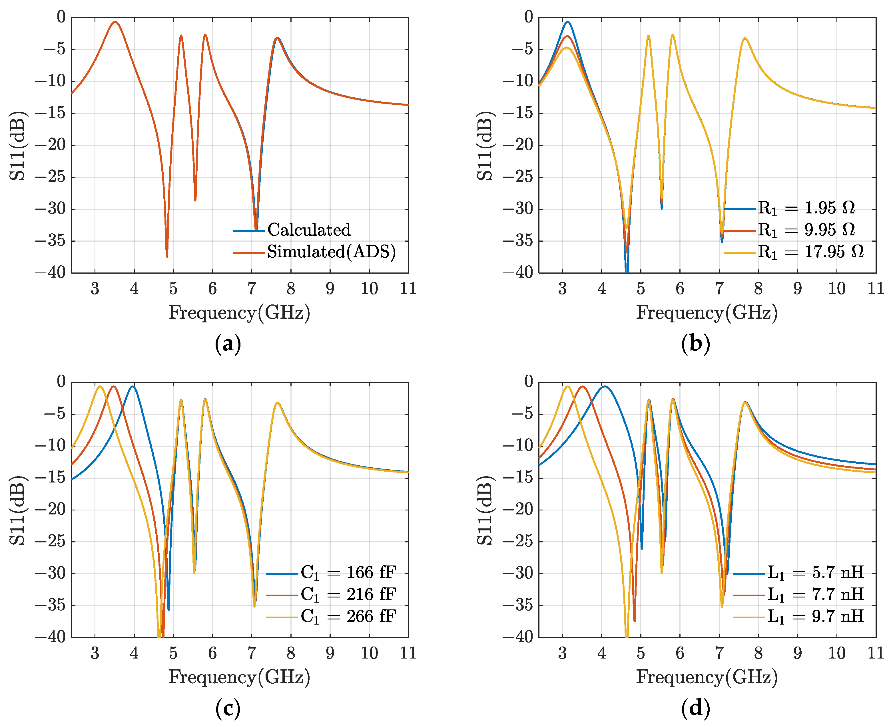
2.3. Input Impedance and Equivalent Circuit Model Analysis

Figure 6a gives the impedance curve of the UWB antenna without the notch-band structures. The real part of the impedance is around 50 Ω and the imaginary part is around 0 Ω. The impedance curve of the UWB antenna with notch-band structures is given in Figure 6b. At 3.5 GHz, 5.2 GHz, 5.8 GHz, and 7.6 GHz, the real part of the impedance is approximately zero and the slope of the imaginary part is positive, showing series resonance characteristics. A low impedance at the feed point results in a mismatch and a band-notch characteristic is observed.
For a series RLC circuit, the bandwidth is defined as the frequency range where the resistance value is less than 1/0.707 times the minimum resistance value. The resistance can also be derived from the simulation results in Figure 6. The lumped element value can be obtained by the following equation and is listed in Table 1:
Q 0 = f 0 BW
Q 0 = 1 2 π f 0 RC
f 0 = 1 2 π LC
Figure 7 shows the equivalent circuit model of the proposed antenna. According to Figure 7, S11 of the equivalent circuit model can be obtained from the Equations (6)–(8). Figure 8a shows the S11 curve of the circuit model obtained through ADS simulation, which agrees with the S11 parameters calculated by the formula. The circuit parameters are analyzed. Taking the curled C-ring as an example, Figure 8b illustrates that when L1 and C1 are unchanged, the notch frequency and band-stop width of the antenna do not change. Figure 8b shows that both R1 and L1 remain unchanged; the notch-band frequency decreases with the increase of C1. Figure 8d depicts that when R1 and C1 remain unchanged, the frequency of the notch band and notch width decrease with the increase of L1. From the above rule, it can be concluded that when the notch frequency needs to be changed, only the capacitance of the structure needs to be changed. When the notch width needs to be changed, it is necessary to change the L of the structure first to obtain a suitable notch width, then change C to move the notch to the appropriate frequency.
Z i = R i + j ω L i + 1 j ω C i
1 Z i n = i = 1 5 1 Z i
S 11 = Z i n Z 0 Z i n + Z 0

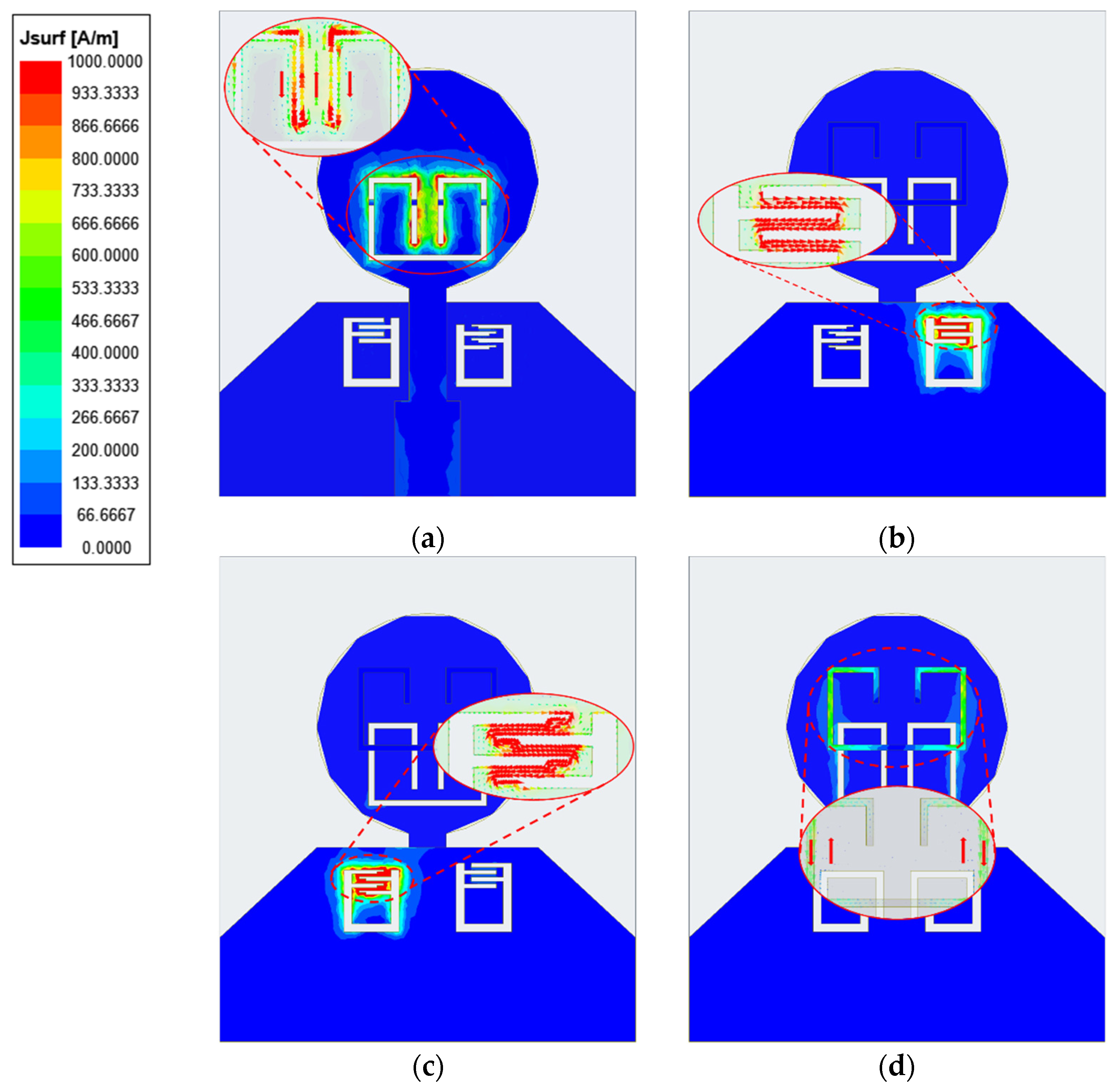
2.4. Performance Analysis and Current Distribution

As shown in Figure 9a, compared with the C-shaped slot without branches, the slot with branches has a lower frequency, narrower notch bandwidth characteristics, and higher VSWR, which helps filter narrow-band signals. In Figure 9b, the ground plane loaded with single C-shaped slots, nested C-shaped slots, and interdigital inductance slots is compared when those slots occupy the same area. Two narrow-band WLAN frequencies can be accurately filtered out by interdigital inductance slots and retain the valuable frequencies, and it is also more compact.
To further study the feature of the band-notched antenna, several parameters of the band-stop structures are investigated in Figure 10. When the L8 is changed from 4.2 mm to 4.8 mm, the band-stop frequency will shift to the low frequency due to the longer electrical length. When W7 changes from 7.5 mm to 9.5 mm, the rising edge of VSWR hardly changes, and the falling edge shifts, which leads to the notch bandwidth increasing from 0.38 GHz to 0.56 GHz. The distance of the curled C-shaped slot’s tail branches controls the band-stop’s width but has little effect on the rising edge of VSWR. From the analysis in Figure 10c,d, and Section 2.3, the essence of increasing L8 is to increase the equivalent capacitance of curled C-shaped slot. The essence of increasing L7 is to reduce the structure’s equivalent inductance and increase the structure’s equivalent capacitance. By choosing the length and distance of tail branches of the slot correctly, the band-notched feature can be controlled efficiently.
The length and width of the interdigital inductance slots at the interdigital position are analyzed in Figure 10. When the interdigital width Lb1 ranges from 0.1 to 0.4 mm, the center frequency of the band-stop and the band-stop width has significantly changed. When the interdigital length Wb1 is from 2.6 to 2.9 mm, the band-stop frequency and band-stop width also change, but the change is small. From the analysis in Figure 11c,d, and Section 2.3, increasing Lb1 reduces the equivalent capacitance of the interdigital inductance slot. The essence of increasing Wb1 is to reduce the equivalent capacitance of the structure. The band-stop parameter can be controlled by modifying these two parameters simultaneously, or the two parameters can be combined to form a stepped interdigital inductance slot, such as the structure in Figure 4d. Using interdigital inductance slots and the added tail branch in the general C-shaped structure makes it possible to filter out the interference frequency band more accurately and achieve high selectivity of the notch.
The final antenna size is: L=35 mm, W = 30 mm, L1 = 6 mm, W1 = 3.7 mm, L2 = 2.6 mm, W2 = 0.4 mm, L3 = 7 mm, W3 = 10 mm, L4 = 7.5 mm, W4 = 16 mm, L5 = 14 mm, W5 = 3.5 mm, L6 = 30.9 mm, W6 = 0.4 mm, L7 = 6 mm, W7=8.6 mm, L8=4.8 mm, W8=2.7 mm, L9 = 6.9 mm, W9 = 4.7 mm, R = 8 mm, La = 4.5 mm, Wa = 4 mm, La1 = 0.35 mm, Wa1 = 2.9 mm, La2 = 0.3 mm, Wa2 = 1.8 mm, La3 = 0.15 mm, Wa3 = 0.6 mm, Lb =4.97 mm, Wb=4 mm, Lb1 = 0.3 mm, Wb1 = 2.9 mm, Lb2 = 2.57 mm, Wb2 = 0.6 mm, t = 1.575 mm.
Figure 12b,c show the antenna’s surface current distribution for the two frequency bands used by WLAN. When the antenna works at 5.2 GHz and 5.8 GHz, most of the current is concentrated at the interdigital resonant structure of the interdigital resonant slots. The structure resonates around 5.2 GHz and 5.8 GHz, and the energy cannot be radiated effectively, so a band stop is formed. Figure 12a,d show the surface current distribution of the antenna working at 3.5 GHz and 7.6 GHz. For 3.5 GHz, the current directions are opposite along the inside and outside of slot (a), and the currents are canceled by each other, so the antenna does not radiate, the surface current is concentrated in the curled C-shaped slot, and a frequency notch is achieved around the 3.5 GHz [23]. When the antenna works at 7.6 GHz, the current direction generated by the curled split-ring resonant on the backside of the antenna is opposite to the current direction generated by the corresponding position on the front side of the antenna. Thus, the currents in opposite directions cancel each other out, causing energy to be stored in the curled split-ring resonator rather than radiated into the air.

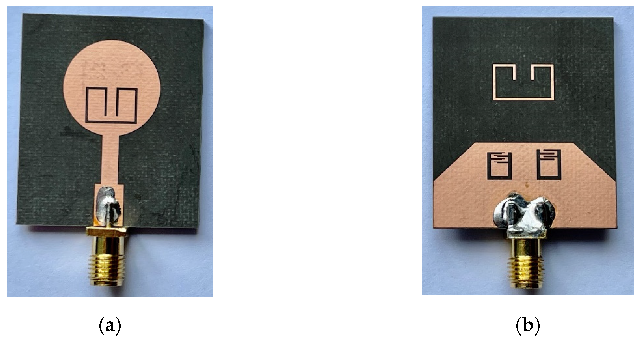
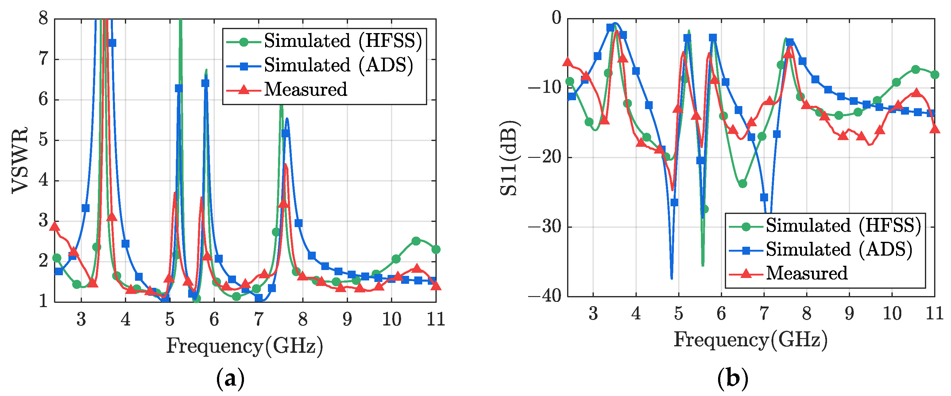
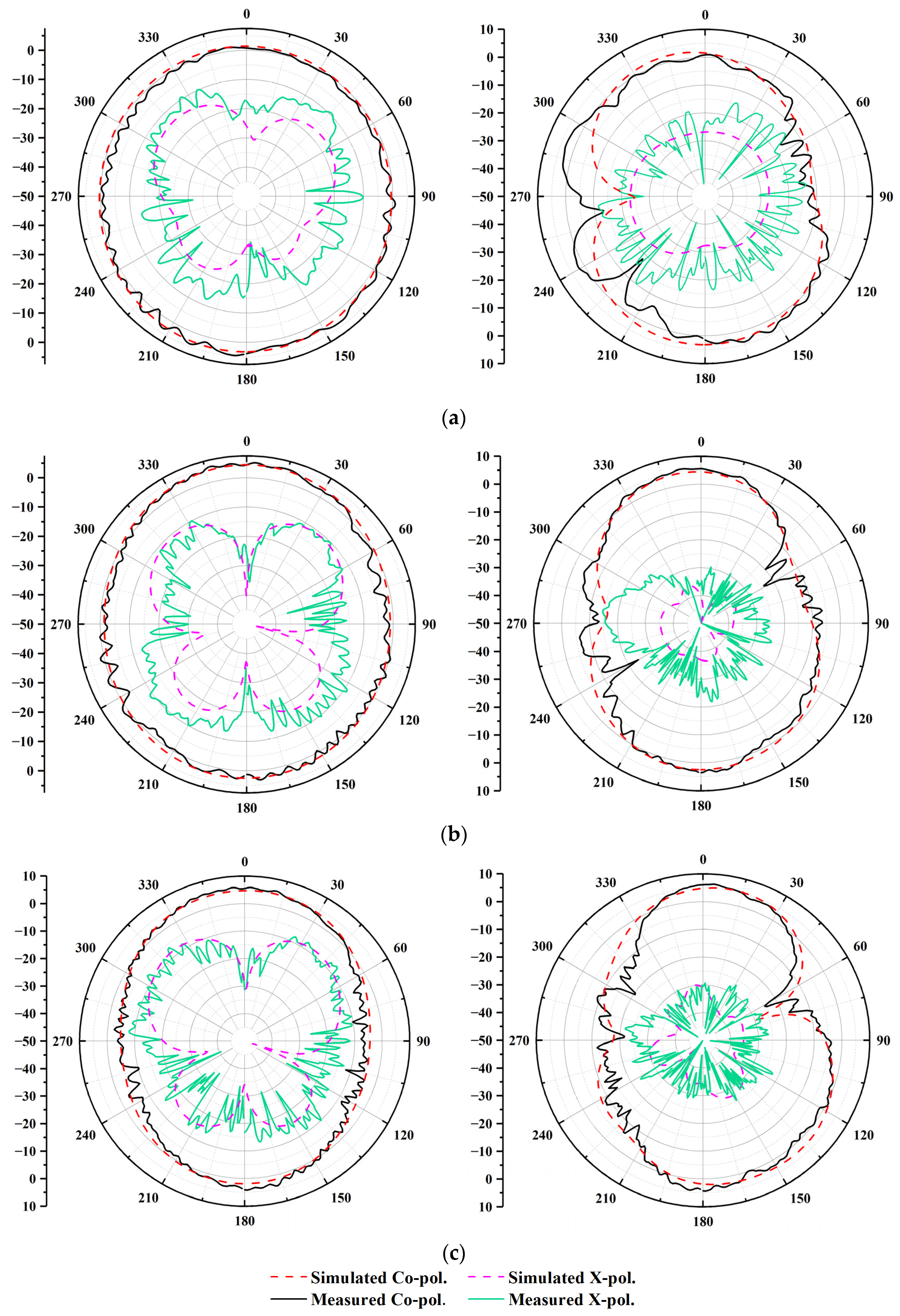
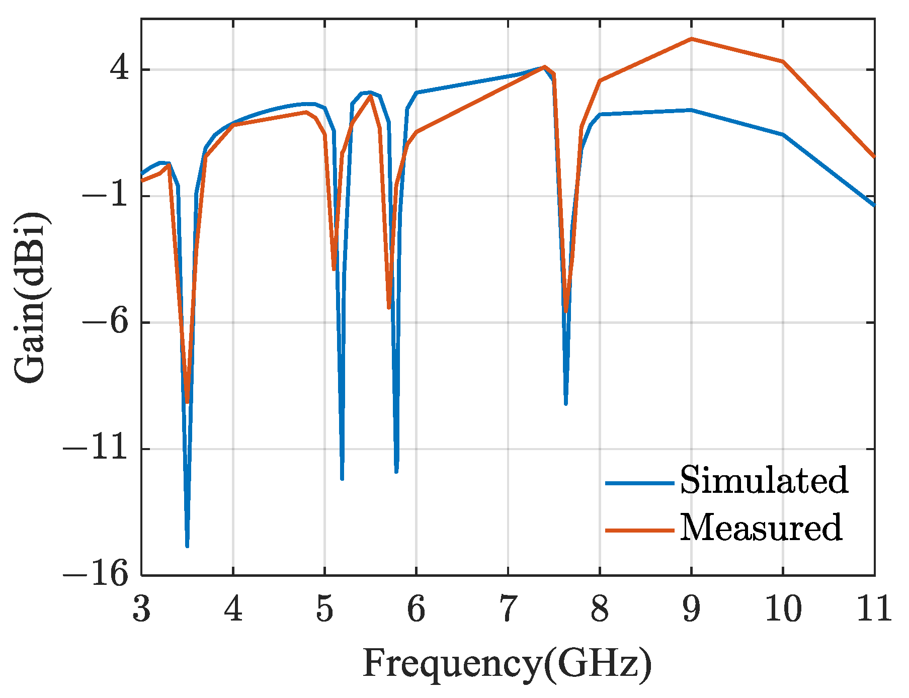
3. Measurement and Discussion

The antenna model is fabricated and tested to verify the actual performance of the designed antenna. The processed object is shown in Figure 13, a vector network analyzer measures the VSWR of the antenna, and the far-field pattern of the antenna is measured in an anechoic chamber.
Figure 14 shows the simulated and measured VSWR and S11 of the designed antenna. The green line is the data obtained from the antenna simulation using HFSS, the blue line is the data obtained from the antenna equivalent circuit model simulation using ADS, and the red line is the measured data. It can be observed that the center frequency of the notch in the actual measurement has a certain frequency offset, which may be caused by the tolerance generated during manufacture and the welding of the antenna connector. The measurement shows that the antenna can achieve frequency coverage of 2.9–11 GHz and produce four band rejections of 3.38–3.75 GHz, 5.01–5.25 GHz, 5.63–5.86 GHz, and 7.45–7.82 GHz.
Figure 15 shows the antenna patterns in the three frequency bands of 6 GHz, 8 GHz, and 10 GHz, respectively. In these frequency bands, the radiation pattern of the X-Z plane antenna is almost omnidirectional. A dipole-like radiation pattern can be observed on the Y-Z plane, but the antenna pattern is not entirely symmetrical. The unsymmetrical pattern is because the two interdigital inductance slots etched at the ground are not identical, making the antenna itself asymmetrical.
In addition, the gain of the antenna is given in Figure 16. The antenna’s gain decreases rapidly in the notch band frequency, reaching minimum points at 3.5 GHz, 5.1 GHz, 5.7 GHz, and 7.63 GHz, respectively. Furthermore, the antenna’s maximum gain reaches more than 4 dBi, which proves that the antenna realizes the quadruple band stops.
Finally, it can be seen from Table 2 that the deviation of the filtering frequency of the antenna used in this paper can be controlled by 3%. The bandwidth of narrow band-stops can be controlled at 0.24 and 0.23 GHz, and the available frequency band 5.25–5.63 GHz is reserved. The antenna shows good performance in both frequency errors and bandwidth errors.

4. Conclusions

In this paper, a novel microstrip-fed monopole printed antenna with quadruple notched bands has been proposed and discussed. The antenna uses a circular radiating patch to achieve broadband characteristics. Two interdigital resonant slots, a curled C-shape slot, and a curled split-ring resonant ring are used to realize quadruple-notched bands. Finally, by adjusting their structural parameters, the antenna achieves notch characteristics of 3.38–3.75 GHz, 5.01–5.25 GHz, 5.63–5.86 GHz, and 7.45–7.82 GH; interference from WiMAX, WLAN, and downlinks of X-band satellite communication are effectively avoided. The antenna shows good omnidirectionality, good gain, and good filtering accuracy in the UWB frequency range. Based on the above considerations, the antenna proposed in this paper is expected to be a good candidate for UWB communication systems.

Author Contributions

C.L. participated in the structure design and optimization, data analysis, simulation, and measurement; Y.W. and Z.D. participated in background research and feasibility analysis; Z.D. and K.D. provided assistance for writing and revision of the paper. All authors have read and agreed to the published version of the manuscript.

Funding

The project was supported by the Fund of State Key Laboratory of Information Photonics and Optical Communications (Beijing University of Posts and Telecommunications) (No. IPOC2022ZZ02), China.

Data Availability Statement

Not applicable.

Conflicts of Interest

The authors declare no conflict of interest.

References

  1. Elmansouri, M.A.; Friedrichs, G.R. An X-Band Through Ka-Band Thinned All-Metal Vivaldi Phased Array. IEEE Trans. Antennas Propag. 2021, 69, 7613–7623. [Google Scholar] [CrossRef]
  2. Masoumi, M.; Dalili, O.; Hamid, R.; Mohammadi Shirkolaei, M. Substrate integrated waveguide leaky wave antenna with circular polarization and improvement of the scan angle. Microw. Opt. Technol. Lett. 2022, 64, 137–141. [Google Scholar] [CrossRef]
  3. Mohammadi Shirkolaei, M.; Ghalibafan, J. Magnetically scannable slotted waveguide antenna based on the ferrite with gain enhancement. Waves Random Complex Media 2021, 1–11. [Google Scholar] [CrossRef]
  4. Moayyed, F.; Dalili, O.; Hamid, R.; Mohammadi Shirkolaei, M. High Gain and Wideband Multi-Stack Multilayer Anisotropic Dielectric Antenna. Prog. Electromagn. Res. Lett. 2021, 99, 103–109. [Google Scholar] [CrossRef]
  5. Mohammadi Shirkolaei, M.; Dalili Oskouei, H.R.; Abbasi, M. Design of 1*4 Microstrip Antenna Array on the Human Thigh with Gain Enhancement. IETE J. Res. 2021, 1–7. [Google Scholar] [CrossRef]
  6. Holland, S.S.; Schaubert, D.H.; Vouvakis, M.N. A 7–21 GHz Dual-Polarized Planar Ultrawideband Modular Antenna (PUMA) Array. IEEE Trans. Antennas Propag. 2012, 60, 4589–4600. [Google Scholar] [CrossRef]
  7. Li, P.; Liang, J.; Chen, X.D. Study of printed elliptical/circular slot antennas for ultrawideband applications. IEEE Trans. Antennas Propag. 2006, 54, 1670–1675. [Google Scholar] [CrossRef]
  8. Zhong, Z.P.; Liang, J.J.; Fan, M.L.; Huang, G.L.; He, W.; Chen, X.C.; Yuan, T. A compact CPW-fed UWB antenna with quadruple rejected bands. Microw. Opt. Technol. Lett. 2019, 61, 2795–2800. [Google Scholar] [CrossRef]
  9. Li, W.T.; Shi, X.W.; Hei, Y.Q. Novel planar UWB monopole antenna with triple band-notched characteristics. IEEE Antennas Wirel. Propag. Lett. 2009, 8, 1094–1098. [Google Scholar]
  10. Li, Y.; Yang, X.; Liu, C.; Jiang, T. Compact CPW-fed ultra-wideband antenna with band-notched characteristic. Electron. Lett. 2010, 46, 1533–1534. [Google Scholar] [CrossRef]
  11. Li, L.; Nan, J.; Liu, J.; Tao, C. A compact UWB antenna with triple band notch reconfigurability. Int. J. Microw. Wireless Technol. 2021, 13, 826–832. [Google Scholar] [CrossRef]
  12. Chu, H.; Lan, S.; Qiu, J.; Fu, Y. Design and investigation of a compact slot antenna with WLAN band rejection for UWB systems. In Proceedings of the 2016 IEEE International Symposium on Antennas and Propagation (APSURSI), Fajardo, PR, USA, 6 June–1 July 2016; pp. 1773–1774. [Google Scholar]
  13. Li, X.P.; Xu, G.; Ma, M.R.; Duan, C.J. UWB dual-band-notched lanky-leaf-shaped antenna with loaded half-square-like slots for communication system. Electronics 2021, 10, 1991. [Google Scholar] [CrossRef]
  14. Sarkar, D.; Khan, T.; Talukdar, F.A. Multi-adaptive neuro-fuzzy inference system modelling for prediction of band-notched behaviour of slotted-UWB antennas optimised using evolutionary algorithms. IETMicrow. Antennas Propag. 2020, 14, 1396–1403. [Google Scholar] [CrossRef]
  15. Horestani, A.K.; Shaterian, Z.; Naqui, J.; Martin, F.; Fumeaux, C. Reconfigurable and tunable S-shaped split-ring resonators and application in band-notched UWB antennas. IEEE Trans. Antennas Propag. 2016, 64, 3766–3776. [Google Scholar] [CrossRef]
  16. Siddiqui, J.Y.; Saha, C.; Sarkar, C.; Shaik, L.A.; Antar, Y. Ultra-wideband antipodal tapered slot antenna with integrated frequency-notch characteristics. IEEE Trans. Antennas Propag. 2018, 66, 1534–1539. [Google Scholar] [CrossRef]
  17. Luo, S.; Chen, Y.; Wang, D.; Liao, Y.; Li, Y. A monopole UWB antenna with sextuple band-notched based on SRRs and U-shaped parasitic strips. AEU-Int. J. Electron. Commun. 2020, 120, 153206. [Google Scholar] [CrossRef]
  18. Zaker, R.; Ghobadi, C.; Nourinia, J. Bandwidth enhancement of novel compact single and dual band-notched printed monopole antenna with a pair of L-shaped slots. IEEE Trans. Antennas Propag. 2009, 57, 3978–3983. [Google Scholar] [CrossRef]
  19. Hong, C.Y.; Ling, C.W.; Tarn, I.Y.; Chung, S.J. Design of a planar ultrawideband antenna with a new band-notch structure. IEEE Trans. Antennas Propag. 2007, 55, 3391–3397. [Google Scholar] [CrossRef]
  20. Jiang, W.; Che, W. A novel UWB antenna with dual notched bands for WiMAX and WLAN applications. IEEE Antennas Wirel. Propag. Lett. 2012, 11, 293–296. [Google Scholar] [CrossRef]
  21. Peng, Y.; Zhang, W.X. Compact sub-wavelength microstrip band-reject filter based on inter-digital capacitance loaded loop resonators. Microw. Opt. Technol. Lett. 2010, 52, 166–169. [Google Scholar] [CrossRef]
  22. Lin, X.Q.; Cui, T.J. Controlling the bandwidth of split ring resonators. IEEE Microw. Wirel. Compon. Lett. 2008, 18, 245–247. [Google Scholar]
  23. Xu, J.; Shen, D.; Zhang, X.; Wu, K. A compact disc ultrawideband (UWB) antenna with quintuple band rejections. IEEE Antennas Wirel. Propag. Lett. 2012, 11, 1517–1520. [Google Scholar]
  24. Zhu, F.; Gao, S.; Ho, A.T.; Abd-Alhameed, R.A.; See, C.H.; Brown, T.W.; Xu, J. Multiple band-notched UWB antenna with band-rejected elements integrated in the feed line. IEEE Trans. Antennas Propag. 2013, 61, 3952–3960. [Google Scholar] [CrossRef] [Green Version]
  25. Emadian, S.R.; Ahmadi-Shokouh, J. Very small dual band-notched rectangular slot antenna with enhanced impedance bandwidth. IEEE Trans. Antennas Propag. 2015, 63, 4529–4534. [Google Scholar] [CrossRef]
  26. Pandey, G.K.; Singh, H.S.; Bharti, P.K.; Meshram, M.K. Design and analysis of Ψ-shaped UWB antenna with dual band notched characteristics. Wirel. Pers. Commun. 2016, 89, 79–92. [Google Scholar] [CrossRef]
  27. Devana, V.K.R.; Rao, A.M. A compact flower slotted dual band notched ultrawideband antenna integrated with Ku band for ultrawideband, medical, direct broadcast service, and fixed satellite service applications. Microw. Opt. Technol. Lett. 2021, 63, 556–563. [Google Scholar] [CrossRef]
  28. Nan, J.C.; Zhao, J.Y. A Compact 8-States Frequency Reconfigurable UWB Antenna. IEEE Access 2021, 9, 144257–144263. [Google Scholar] [CrossRef]
  29. Puri, S.C.; Das, S.; Tiary, M.G. UWB monopole antenna with dual-band-notched characteristics. Microw. Opt. Technol. Lett. 2020, 62, 1222–1229. [Google Scholar] [CrossRef]
  30. Han, L.P.; Cheng, G.; Han, G.R. Reconfigurable ultra-wideband monopole antenna with single-, dual-, and triple-band notched functions. Int. J. RF Microw. Comput. Aided Eng. 2019, 29, e21837. [Google Scholar] [CrossRef]
  31. Sharma, M.; Kumar, R.; Kaur, P. Design and analysis of on-demand reconfigurable WiMAX / WLAN high isolation 2 × 2 MIMO antenna oriented adjacent/orthogonally for imaging applications in UWB-X band. Int. J. RF Microw. Comput. Aided Eng. 2022, 32, e22928. [Google Scholar] [CrossRef]
  32. Wang, M.Y.; Wang, H.B.; Chen, P. A butterfly-like slot UWB antenna with WLAN band-notch characteristics for MIMO applications. IEICE Electron. Express. 2022, 14, 20220233. [Google Scholar] [CrossRef]
Figure 1. Configuration of the proposed antenna.
Electronics 11 03949 g001
Figure 2. Simulated VSWR of the proposed antenna under different values of corner cut (a) W4 (b) L4.
Electronics 11 03949 g002
Figure 3. Simulated VSWR of the proposed antenna without notched bands in case of different g.
Electronics 11 03949 g003
Figure 4. The geometry of band-notched structures: (a) curled split-ring resonator, (b) curled C-shaped slot, (c) interdigital inductance slots 1, and (d) interdigital inductance slots 2.
Electronics 11 03949 g004
Figure 5. Simulated VSWR of UWB antennas with (a) single band-notched structure and (b) all structures.
Electronics 11 03949 g005
Figure 6. Simulated impedance characteristics of the proposed antennas. (a) Without band notch structures. (b) With band notch structures.
Electronics 11 03949 g006
Figure 7. Equivalent circuit model of the proposed band-notched UWB antenna.
Electronics 11 03949 g007
Figure 8. Simulated S11 of equivalent circuit model under different parameters. (a) Comparison between simulation and calculation. (b) Equivalent resistance R1. (c) Equivalent capacitance C1. (d) Equivalent inductance L1.
Electronics 11 03949 g008
Figure 9. Simulated VSWR of the proposed antenna under different structures. (a) Curled C-shaped slots. (b) Interdigital inductance slot.
Electronics 11 03949 g009
Figure 10. Simulated of the proposed antenna under different values of tail branches of the curled C-shaped slot. (a) VSWR under different Length L8. (b) VSWR under different Distance W7. (c) S11 under different Length L8. (d) S11 under different Distance W7.
Electronics 11 03949 g010aElectronics 11 03949 g010b
Figure 11. Schematic diagram of interdigital inductance slots. (a) VSWR under different Lb1. (b) VSWR under different Wb1. (c) S11 under different Lb1. (d) S11 under different Wb1.
Electronics 11 03949 g011
Figure 12. Simulated magnitude of current distribution at (a) 3.5, (b) 5.2, (c) 5.8, and (d) 7.6 GHz.
Electronics 11 03949 g012
Figure 13. Photos of the antenna prototype. (a) The front of the antenna. (b) The back of the antenna.
Electronics 11 03949 g013
Figure 14. Simulated and measured of the proposed antenna. (a) VSWR. (b) S11.
Electronics 11 03949 g014
Figure 15. Simulated and measured radiation patterns. X-Z Plane (left) and Y-Z Plane (right). (a) 6 GHz, (b) 8 GHz, and (c) 10 GHz.
Electronics 11 03949 g015
Figure 16. Gain of the proposed antenna with notched bands.
Electronics 11 03949 g016
Table 1. Calculated values of lumped elements.
Circuit.BW (MHz)R (Ω)L (nH)C (fF)Q0
Curled C-shaped slot401.957.726687.5
Interdigital inductance
slots 1
409.4937.724.9129.8
Interdigital inductance
slots 2
509.2329.425.6116
Curled split-ring resonator11011.5116.626.269.09
Table 2. Comparison of proposed and reference antenna about unwanted bands and achieved rejection bands.
Ref.UWB Band/GHzSize/mm2Unwanted Bands (Bandwidth)/GHzRejection Bands (Bandwidth)/GHzBand Error/%Bandwidth Error/%
[8]2.7–10.725 × 223.3–3.7 (0.4)3.58–4.32 (0.74)8.5, 16.885
5.15–5.35 (0.2)5.36–5.57 (0.21)4.1, 4.15
5.725–5.825 (0.1)5.98–6.10 (0.12)4.5, 4.720
7.8–8.2 (0.4)8.12–8.85 (0.73)4.1, 7.983
[13]2.8–1032 × 273.3–3.7 (0.4)3.06–3.83 (0.77)7.2, 3.593
5.15–5.35 (0.2)5.05–N/A (N/A)1.9, N/AN/A
5.725–5.825 (0.1)NA–5.96 (N/A)N/A, 2.3N/A
[20]2.8–11N/A3.3–3.7 (0.4)3.3–4.0 (0.7)0, 8.175
5.15–5.35 (0.2)5.05–N/A (N/A)9, N/AN/A
5.725–5.825 (0.1)N/A–5.9 (N/A)N/A, 1.2N/A
[23]2.45–1231.8 × 263.3–3.7 (0.4)3.27–3.57 (0.3)0.9, 3.525
5.15–5.35 (0.2)5.01–5.45 (0.44)2.7, 1.8120
5.725–5.825 (0.1)5.55–6.05 (0.5)3.0, 3.8400
7.25–7.75 (0.5)7.05–7.45 (0.4)2.7, 3.820
8.025–8.4 (0.375)7.83–8.19 (0.36)2.4, 2.54
[24]N/A28.5 × 283.3–3.7 (0.4)3.15–3.62 (0.47)4.5, 2.117.5
5.15–5.35 (0.2)5.1–5.38 (0.28)0.9, 0.840
5.725–5.825 (0.1)5.72–6.12 (0.4)0.1, 5.1300
[25]2.6–2315 × 153.3–3.7 (0.4)3.1–3.9 (0.8)6, 5.4100
5.15–5.35 (0.2)5.1–N/A (N/A)0.9, N/AN/A
5.725–5.825 (0.1)NA–6 (N/A)N/A, 3N/A
[26]2.5–1140 × 373.3–3.7 (0.4)3.2–3.8 (0.6)4.7, N/A50
5.15–5.35 (0.2)5.1–N/A (N/A)1, N/AN/A
5.725–5.825 (0.1)N/A–5.9 (N/A)N/A, 1.3N/A
[27]2.9–23.522 × 165.15–5.35 (0.2)5.39–N/A (N/A)4.7, N/AN/A
5.725–5.825 (0.1)N/A–5.9 (N/A)N/A, 1.3N/A
7.25–7.75 (0.5)7.30–7.75 (0.45)0.7, 010
[28]2.82–13.2522 × 133.3–3.7 (0.4)3.19–4.58 (1.39)3.3, 23.7247
5.47–5.875 (0.4)5.26–6.21 (0.95)3.8, 5.7137
7.9–8.4 (0.5)7.87–8.73 (0.86)0.4, 3.972
[29]2.76–1132 × 303.3–4.2 (0.9)3.45–N/A (N/A)4.5, N/AN/A
4.5–4.8 (0.3)N/A–4.81 (N/A)N/A, 0.2N/A
4.15–5.35 (1.2)5.24–N/A (N/A)26, N/AN/A
5.47–5.725 (0.26)N/A–6.21 (N/A)N/A, 8.5N/A
[30]N/A30 × 263.4–3.69 (0.29)3.21–3.79 (0.58)2.7, 2.7100
5.15–5.35 (0.2)4.65–5.43 (0.78)9.7, 1.5290
7.25–7.75 (0.5)7.15–8.07 (3.42)1.4, 4.1584
[31]3.57–11.724 × 243.3–3.8 (0.5)3.39–3.92 (0.53)2.7, 3.26
5.15–5.35 (0.2)4.43–5.48 (1.05)14, 2.4425
[32]3–1232 × 405.1–5.37 (0.27)5.05–5.35 (0.3)0.9, 0.411
This work2.9–1135 × 303.3–3.7 (0.4)3.38–3.75 (0.37)2.4, 1.37.4
5.15–5.35 (0.2)5.01–5.25 (0.24)2.7, 1.98.3
5.725–5.825 (0.1)5.63–5.86 (0.23)1.6, 0.6120
7.25–7.75 (0.5)7.45–7.82 (0.37)2.8, 0.926
Publisher’s Note: MDPI stays neutral with regard to jurisdictional claims in published maps and institutional affiliations.

