Article

A 0.00426 mm2 77.6-dB Dynamic Range VCO-Based CTDSM for Multi-Channel Neural Recording

1
IMEC, 3001 Leuven, Belgium
2
School of Engineering, University of Edinburgh, Edinburgh EH8 9YL, UK
3
Department of Electrical and Electronic Engineering, Imperial College London, London SW7 2BX, UK
*
Authors to whom correspondence should be addressed.
Electronics 2022, 11(21), 3477; https://doi.org/10.3390/electronics11213477
Submission received: 16 September 2022 / Revised: 19 October 2022 / Accepted: 24 October 2022 / Published: 26 October 2022
(This article belongs to the Special Issue Advanced Analog Circuits for Emerging Applications)

Abstract

:
Driven by needs in neuroscientific research, future neural interface technologies demand integrated circuits that can record a large number of channels of neural signals in parallel while maintaining a miniaturized physical form factor. Using conventional methods, it is challenging to reduce circuit area while maintaining the high dynamic range, low noise, and low power consumption required in the neural application. This paper proposes to address this challenge using a VCO-based continuous-time delta-sigma modulator (CTDSM) circuit, which can record and digitize neural signals directly without the need for front-end instrumentation amplifiers and anti-aliasing filters, which are limited by the abovementioned circuit-area performance tradeoff. Thanks to the multi-level quantization and intrinsic mismatch-shaping capabilities of the VCO-based approach, the proposed first-order CTDSM can achieve comparable electrical performance to a higher-order CTDSM while offering further area and power reductions. We prototyped the circuit in a 22-channel test chip and demonstrate, based on the chip measurement results, that the proposed modulator occupies an area of 0.00426 mm2 while achieving input-referred noise levels of 6.26 and 3.54 µVrms in the action potential (AP) and local field potential (LFP) bands, respectively. With a 77.6 dB wide-dynamic range, the noise and total harmonic distortion meet the requirements of a neural interface with up to 149 mVpp input AC amplitude or up to ±68 mV DC offsets. We also validated the feasibility of the circuit for multi-channel recording applications by examining the impact of cross-channel VCO oscillation interferences on the circuit noise performance. The experimental results demonstrate the proposed architecture is an excellent candidate to implement future multi-channel neural-recording interfaces.

1. Introduction

Multi-channel neural-recording integrated-circuits are essential in today’s electrophysiology tools to enable simultaneous readouts from thousands of neurons in vivo [1,2]. These tools allow neuroscientists to access signals from large neuronal populations across wider brain regions while conducting experiments on freely moving animals, leading to a deeper and more comprehensive understanding of the brain and nervous system [3,4,5,6]. The proliferating demand for large-scale neural interfacing has been driving the development of area-efficient neural-recording circuits, which allow the integration of more parallel recording channels in miniaturized systems on a chip [7,8,9,10,11].
Conventionally, a neural-recording channel consists of at least three circuit blocks: an instrumentation amplifier (IA), an anti-aliasing filter (AAF), and an analog-to-digital converter (ADC) [8,9,10,12,13,14]. In such architecture, the IA and AAF amplify and condition the input signal before the ADC, thus reducing the requirement of the latter. However, the circuit areas of the IA and AAF are difficult to minimize given the low-noise and high-input-impedance requirements; furthermore, the channel dynamic range is limited. In recent years, continuous-time delta-sigma modulators (CTDSM) have been used for the direct digitization of neural signals, which achieved good area efficiency [11,15,16,17,18,19]. CTDSMs have implicit anti-aliasing capabilities and can achieve high-input-impedance and low-noise results [20]. Therefore, it is possible to directly use CTDSMs for neural recording, thus eliminating the need for dedicated instrumentation amplifiers (IAs) and anti-aliasing filters while achieving good area efficiency. Furthermore, the capability to achieve a high dynamic range (DR) makes CTDSMs better candidates for implementing artifact-tolerant neural recording compared with conventional architecture, which can be easily saturated with large input artifacts. In Refs. [16,18], input ranges of 300 mVpp and 148 mVpp were achieved, respectively, which are significantly wider than the input ranges of conventional IA-based front ends, which are typically limited to 10 mVpp [8,9,10,12,13,14].
The suitability of CTDSMs for direct neural recording can be further improved by using phase-domain integration and multi-bit quantization through voltage-controlled oscillators (VCOs) [18,21,22,23,24,25,26]. Such VCO-based approaches allow loop filters and quantizers to operate under a low supply voltage, and they have intrinsic mismatch-shaping capabilities to address the linearity issues in multi-bit modulators. Moreover, they can strongly benefit from CMOS technology scaling, since the integrators and quantizers are fully implemented in the digital domain. Thanks to these advantages, previously reported works have achieved ultra-high DR with good area and power efficiencies. Nevertheless, all the existing works only demonstrated VCO-based neural recording on single-channel designs, while its feasibility for multi-channel neural recording is not yet validated. A potential issue of using a VCO-based architecture for multi-channel neural recording is the coupling of VCO oscillation interferences from the nearby channels. This issue can be significant as the reference voltages and supply lines are typically shared among multiple channels, and the VCO center frequencies will be different across channels. This can result in potential broadband interferences that are more difficult to remove. These effects need to be investigated to validate the suitability of VCO-based readout architectures for multi-channel neural-recording applications.
In this paper, we present the design and experimental results of a VCO-based CTDSM for multi-channel neural recording. The modulator provides first-order noise shaping and 30-level quantization by using 15-stage ring oscillators (ROs), and it was tested in a 22-channel prototype chip. We demonstrate that the modulator can achieve equivalently good input-referred-noise, DR, and input-impedance performances compared with a more complex second-order CTDSM neural-recording front-end with two times the sampling rate [18]. The reduced complexity and sampling rate allows further reductions in circuit area and power consumptions. We also measured the effects of multi-channel VCO oscillation interference on the modulator performance. The results indicate an acceptable increase of noise when multiple channels that are densely placed and have shared reference and supply voltages are operating simultaneously. This proves the design is suitable for the target multi-channel applications.

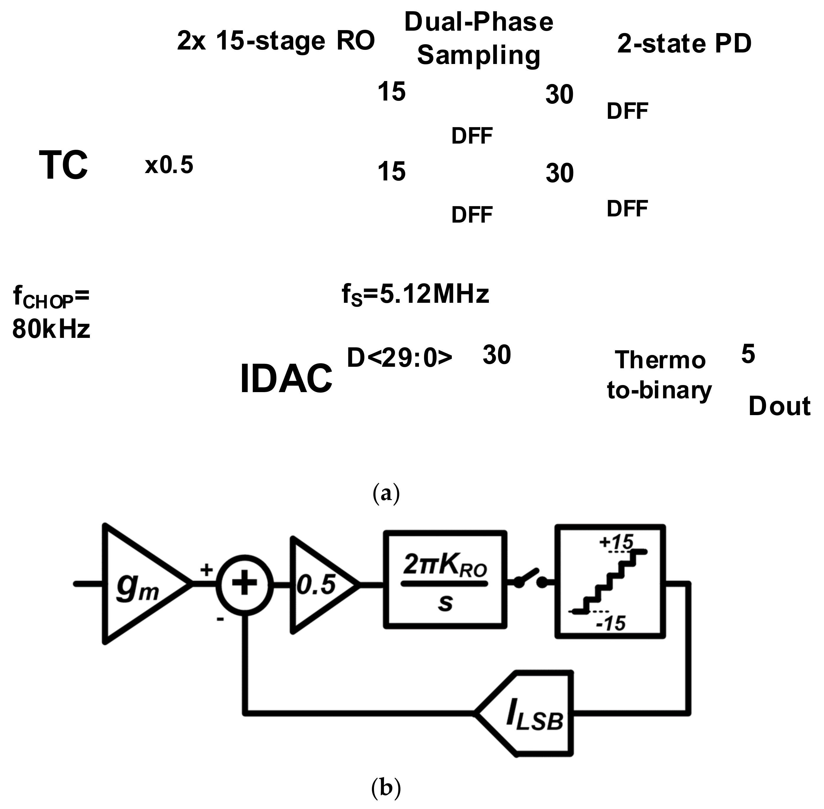
2. Modulator Architecture
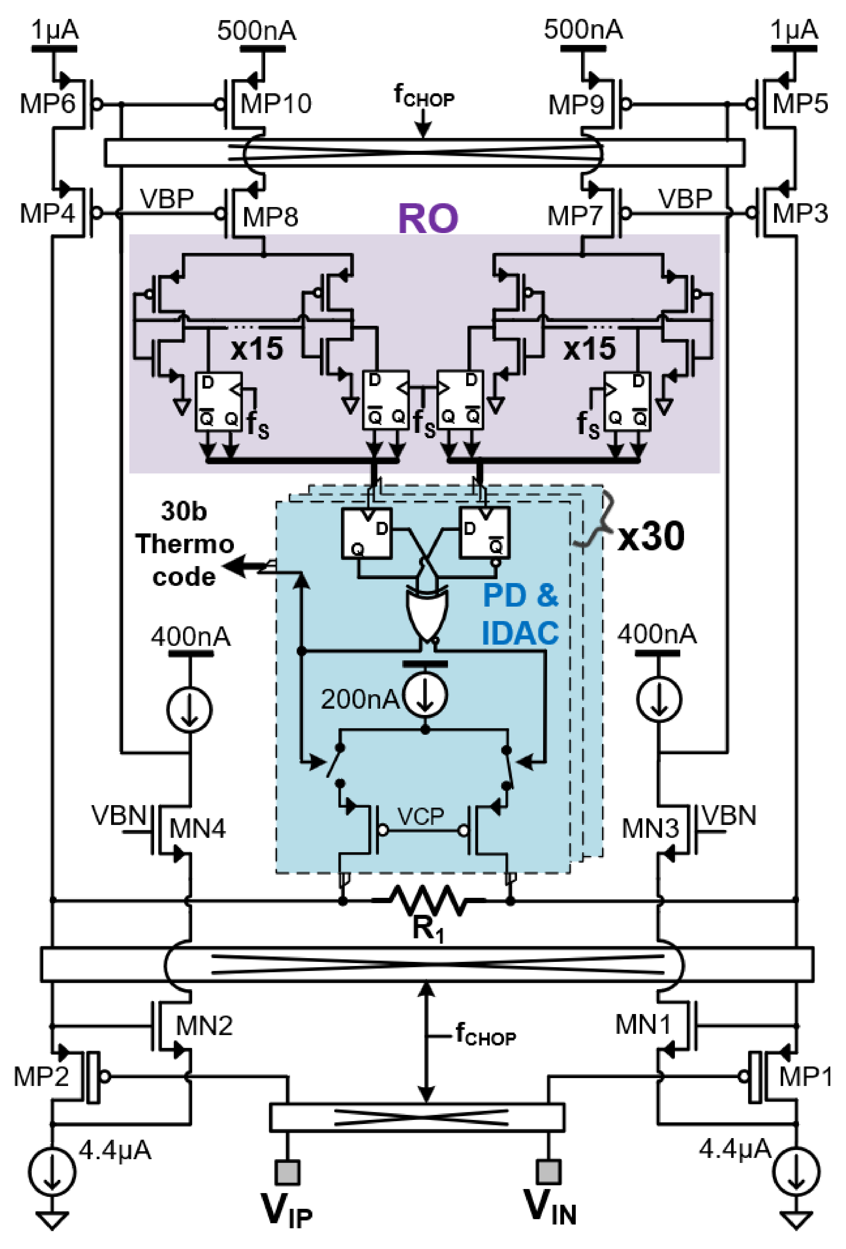
The high-level block diagram of the proposed CTDSM is shown in Figure 1a, while the simplified s-domain diagram is given in Figure 1b. The modulator uses a chopper-stabilized transconductance (TC) amplifier as the input stage, which converts input neural potentials into a current signal. The difference between the input current and the current-mode digital-to-analog converter (IDAC) feedback is halved and then used to modulate the supply current of a pair of 15-stage ROs. The RO outputs are sampled with D flip flops (DFFs), and both the non-inverting and the inverting outputs of the DFFs are fed to an array of two-state phase detectors (PD). This results in an effective 30-level quantization. The 30-level quantized results are thermometer-coded, and they are fed back through the IDAC as well as sent to the output through a thermometer-to-binary (Th2Bi) logic. A list of high-level design parameters is summarized in Table 1. The feed-in coefficient b and feedback coefficient a are derived with the following equations:
b   =   2 g m · 0.5 · 2 π K R O f s
a   =   2 I L S B · 0.5 · 2 π K R O f s
The modulator is designed to record both local field potentials (LFPs) and action potentials (APs), covering a signal bandwidth of 10 kHz. The AP and LFP signal amplitudes are typically up to 10 mVpp [1,2,8,9]; however, this design targets a wider input range (up to ~150 mVpp) to accommodate electrode DC offsets and tolerate stimulation/movement artifacts. Therefore, the TC stage, the IDAC least significant bit (ILSB), and the number of quantization levels (which also defines the number of RO stages) are chosen to obtain this required input voltage range, which is determined by N*ILSB/gm. The modulator provides first-order noise shaping with an oversampling ratio (OSR) of 256 and 30-level quantization. Thus, ~1 µVrms total input-referred in-band quantization noise can be achieved, which is given by
V Q N ,   i 2 ¯ = π 2 a 2 36 O S R 3 b 2
To meet the noise requirements of a neural-recording application, the readout-circuit noise needs to be minimized. Therefore, in this design, the value of gm is chosen as the optimal trade-off between circuit noise and power consumption.

3. Schematic Design

The schematic design of the modulator is shown in Figure 2, which includes all blocks except the Th2Bi logic. Transistors MN1-4 and MP1-10 form a chopper-stabilized current-balancing TC stage, with input impedance boosting achieved using the bootstrapping transistors MN1-2 [18]. The input transistors MP1-2 are thick-oxide devices to avoid gate leakage. The gm is defined by resistor R1, which has a value of 32.7 kΩ. The IDAC feedback currents are injected at the two terminals of R1, and the voltage difference across the two terminals is a copy of the input voltage because of the flipped-voltage-follower structure formed by MP1-6 and MN1-4. Therefore, the input voltage is converted to a current by R1, and the difference between the converted input current and the IDAC feedback current flows through transistors MP3-6, gets copied to MP7-10 with a 2:1 ratio, and is finally injected to the top lines of the two 15-stage ROs. The two ROs are pseudo-differential and both the rising and the falling edges of their outputs can trigger the PDs. In this way, the 30-level quantization is achieved. The quantized outputs from the 30 PDs are fed to the IDAC, which has 30 current-steering elements. Compared with the input TC stage in Ref. [18], this design does not require common-mode feedback circuits, which is another advantage of the VCO-based approach.
The total static current consumption of the modulator is 9.8 µA. The PDs will consume additional dynamic power, which depends on the sampling rate. In this design, the
IDAC and the ROs are embedded in the TC stage and do not consume additional power. The currents of the IDAC (i.e., 15×200 nA on each side when the input voltage difference is 0 V) contribute to the biasing of the input transistor (MP1-2), and the ROs are directly biased with the TC output current. A lower RO free-running frequency (fRO) is preferred to reduce the dynamic power consumption of the ROs and PDs, which can be achieved by reducing the TC common-mode (CM) output current or increasing the RO loading capacitance at each inverter stage. The latter is realized by increasing the inverter gate lengths, which enlarges the RO area but reduces the flicker noise. In this design, the TC CM output current is 0.5 µA and, thus, a 370 kHz fRO is achieved while preserving a small RO area. Because ILSB is 200 nA and it determines the RO frequency modulation index, further reducing the TC CM output current will induce large voltage variations on the RO top-line voltage, thus increasing the non-linearity and causing errors due to unmatched logic levels with the following DFFs.

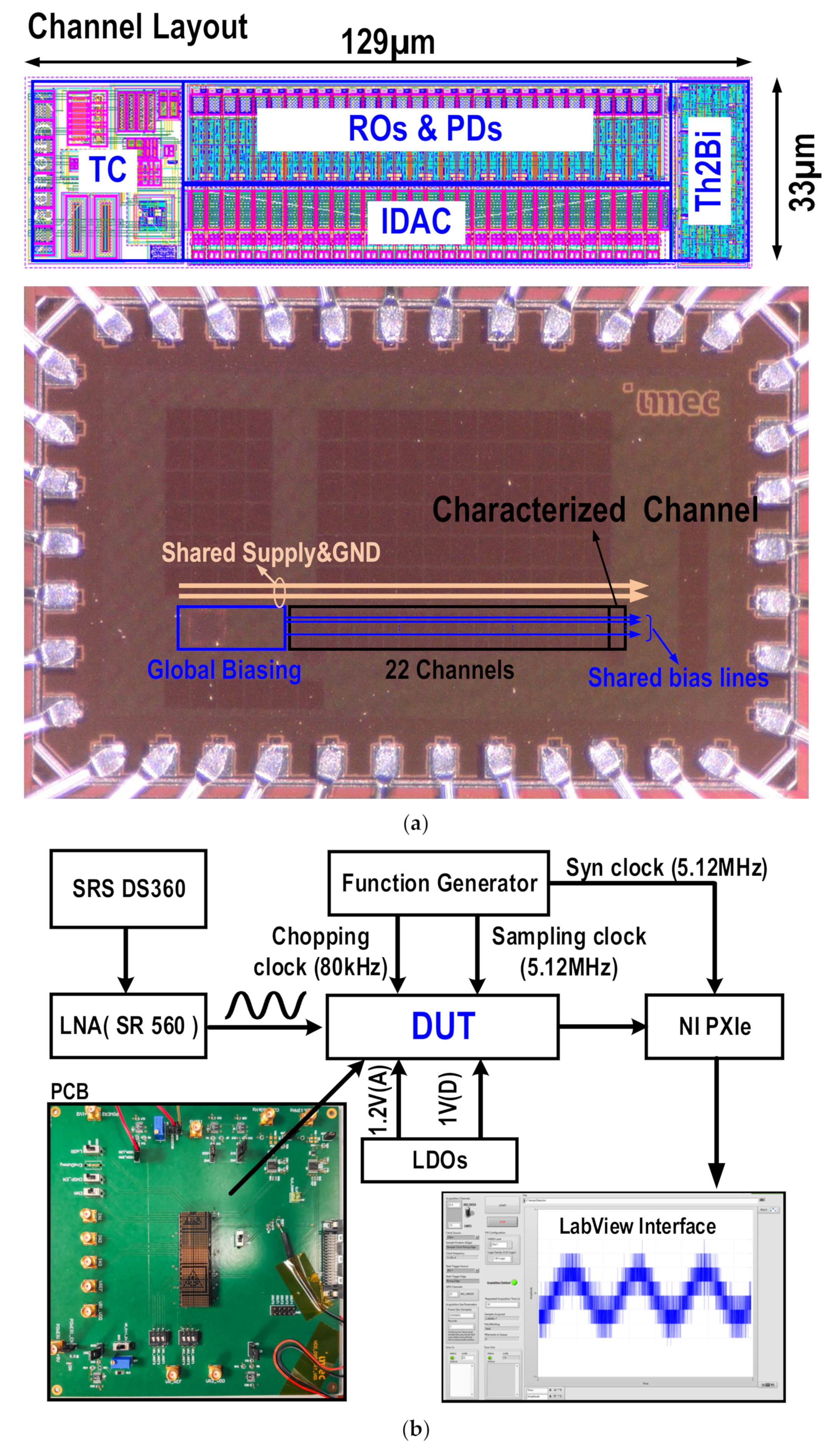
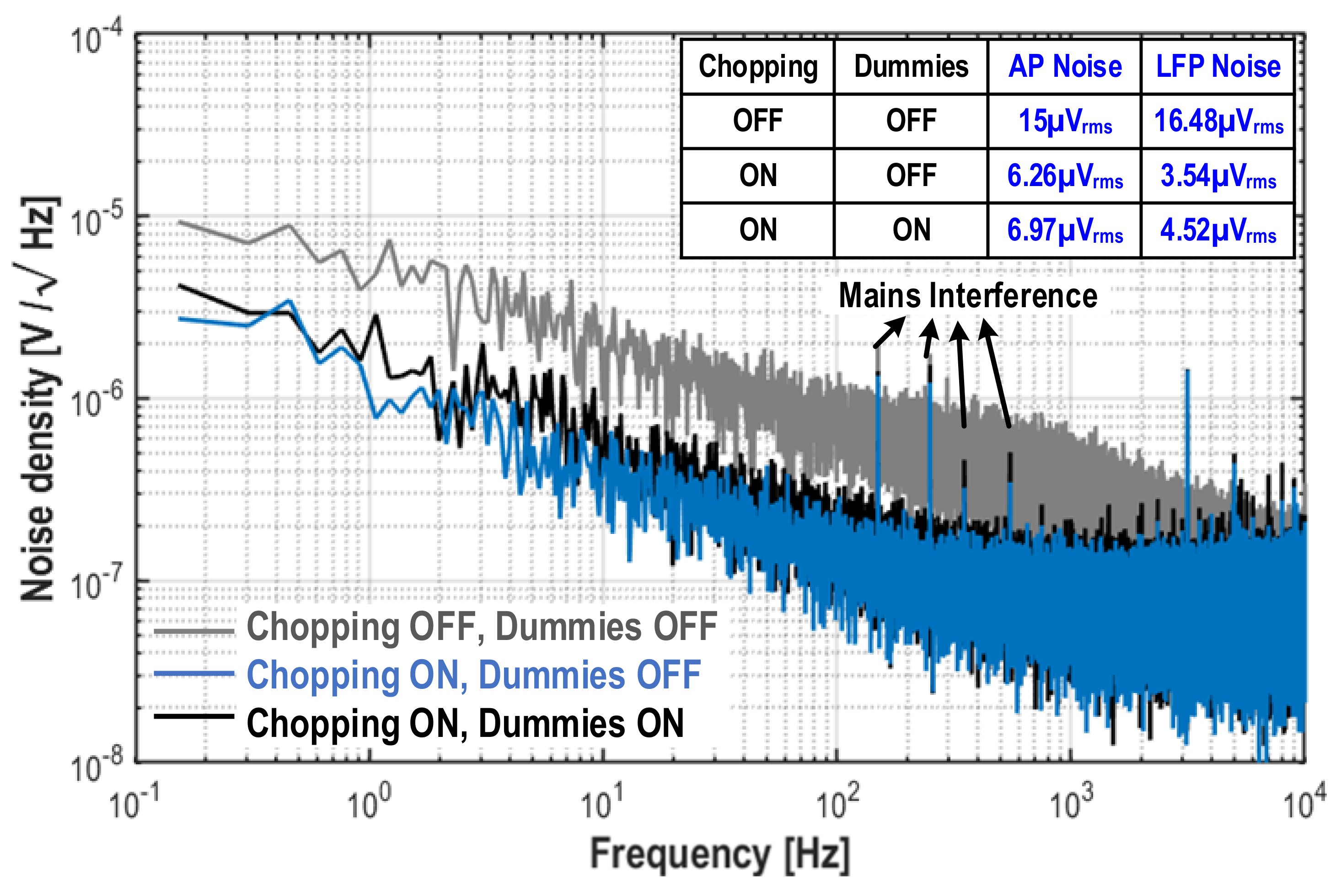
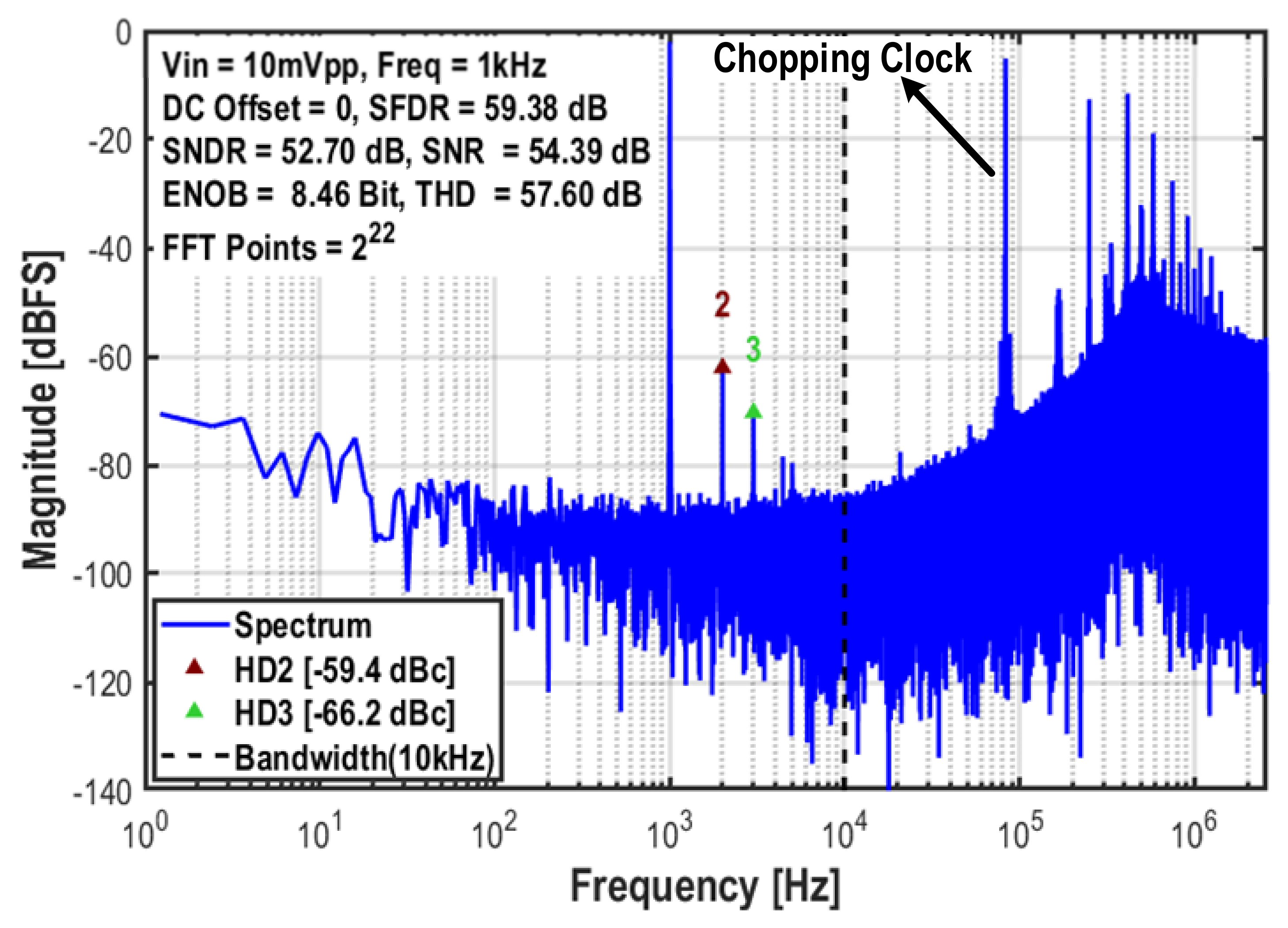
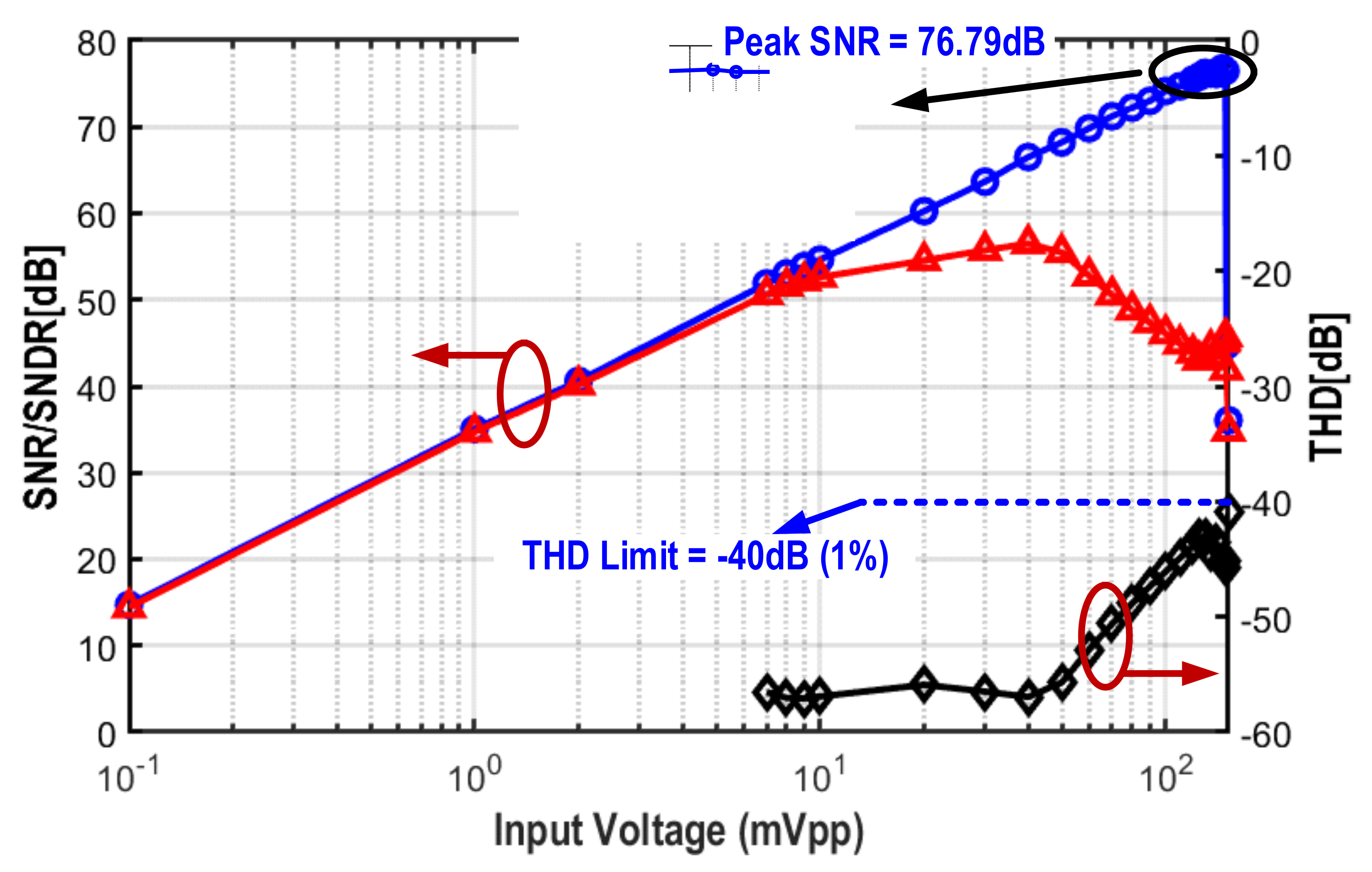
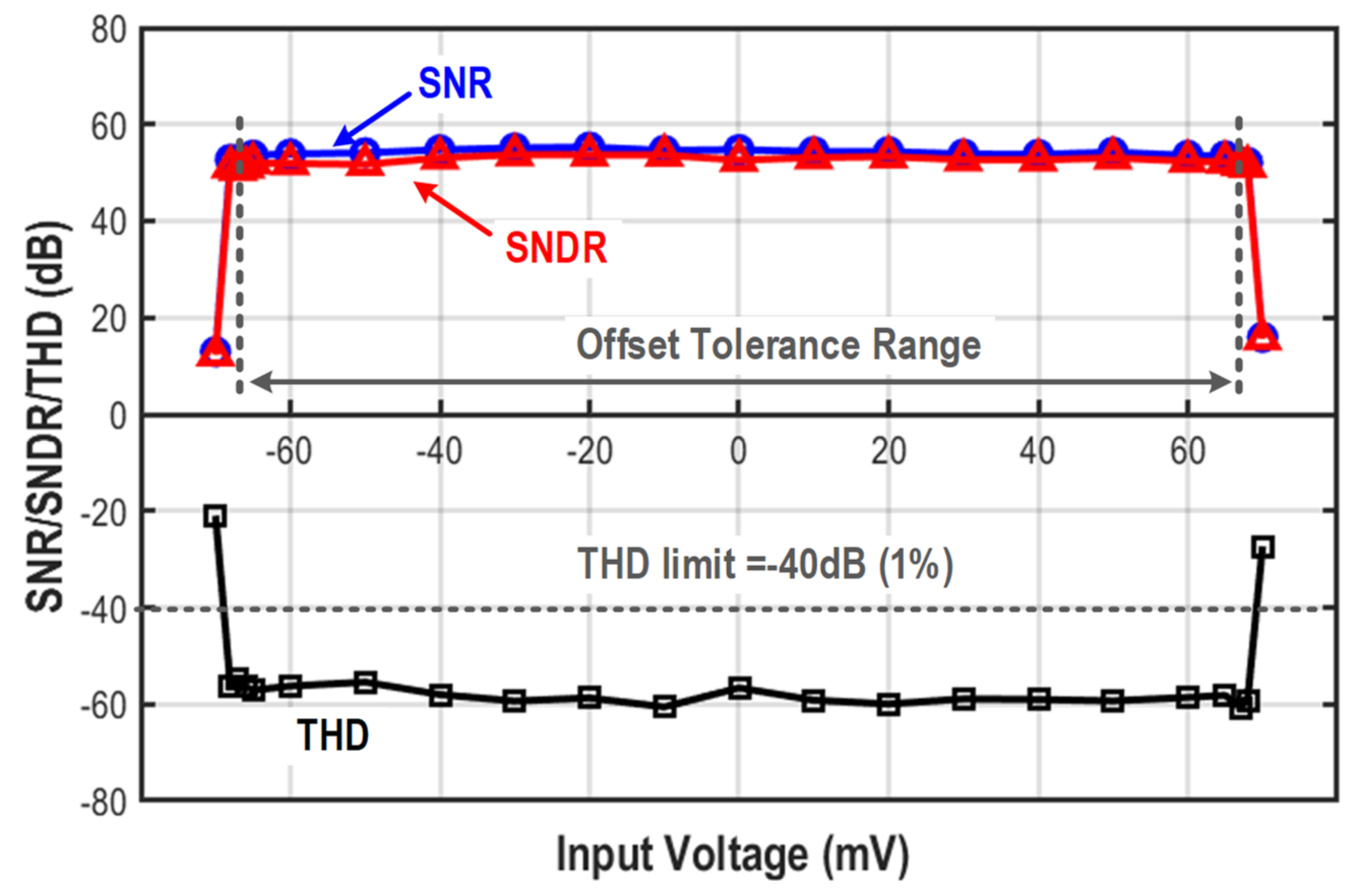
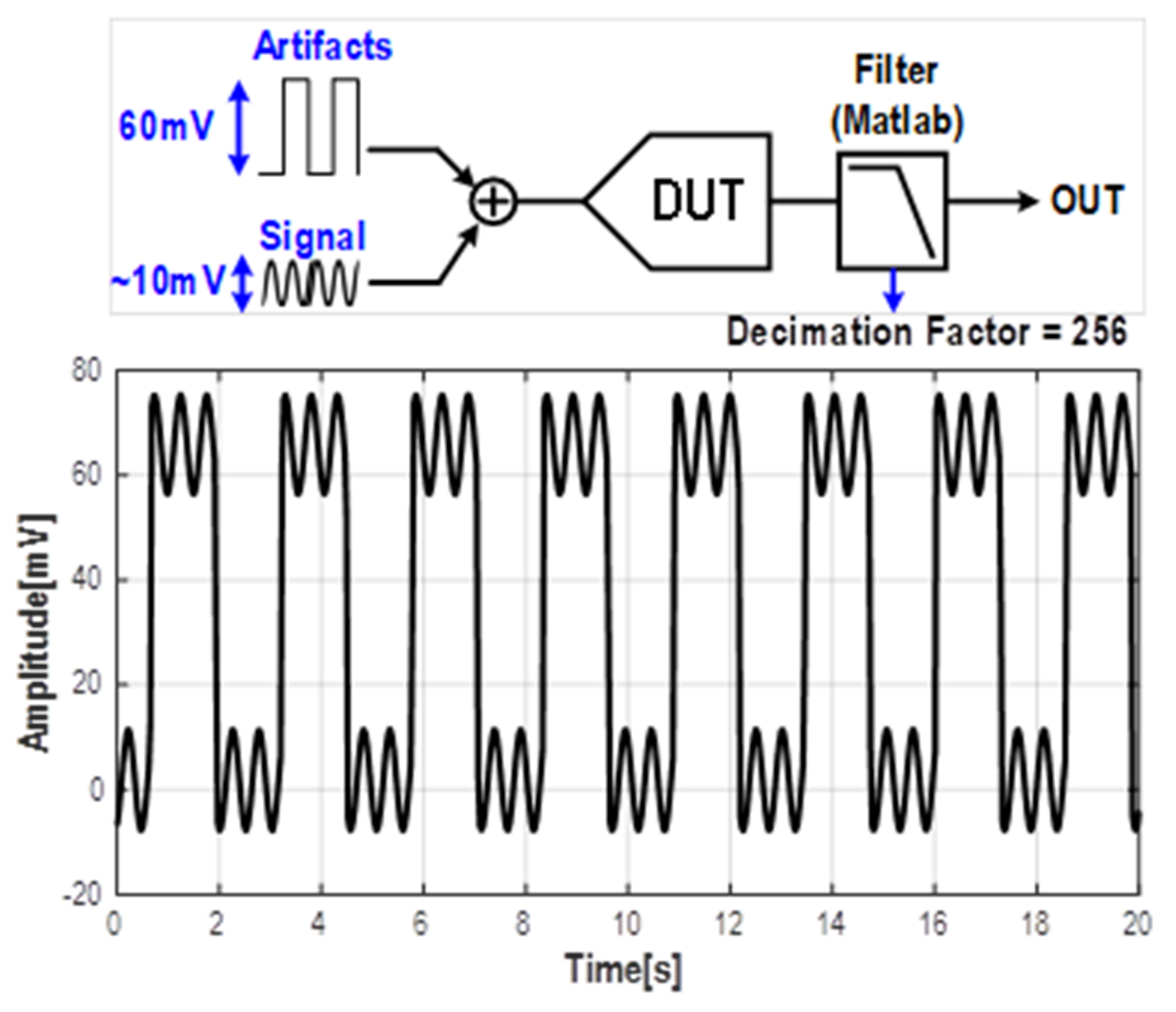
4. Results and Discussion

A prototype chip was implemented and fabricated using a 55 nm CMOS technology. The chip micrograph and channel layout details are shown in Figure 3a. Each channel occupies an area of 129 µm × 33 µm. In order to evaluate the influence of the neighboring channels (i.e., VCO oscillation interferences) on the proposed CTDSM readout performance, a total of 22 channels sharing the same biasing voltages and supplies were implemented on the chip. All the channels share the same biasing, supply voltages, and ground lines, which are distributed from left to right to replicate the layout constraints in ultra-dense neural probes [8,9]. In this proof-of-concept prototype, the outputs of only 3 out of the 22 channels are accessible for characterizations. These three channels include two that are right next to the global biasing block (these are the best-case channels) and one that is the farthest from the global biasing block (this is the worst-case channel). In this work, we used the setup shown in Figure 3b to characterize the three channels. The worst-case channel will pick up the highest noise coupling and interferences from the other channels, and the impacts of these coupling effects and interferences can be quantitatively evaluated by comparing the results in two cases: (i) when all other channels are enabled and (ii) when all other channels are disabled. To test the chip, we developed a custom-printed circuit board using Altium and used a National Instrument module to acquire and analyze the chip output data, while the required decimation filter was implemented in software.
The measured noise spectrum and the integrated input-referred noise in the LFP (0.5–1000 Hz) and AP (0.3–10 kHz) bands are shown in Figure 4. The effectiveness of the chopper-stabilization technique is demostrated in this measurement. When the choppers in the TC stage were disabled, the noise is 2.4 times higher in the AP band and 4.65 times higher in the LFP band. Note that a residual low-frequency flicker noise is visible in the noise spectrum, which is because the transistors that form the PMOS current mirror in the TC stage (MP5-6 and MP9-10) are not chopped. This is a design choice made to avoid the aliasing of high-frequency-shaped quantization noise in the IDAC feedback, as elaborated in Ref. [18]. From these results, we can also conclude that the AP and LFP noise only increases by 11.3% and 27.7%, respectively, in the worst-case channel when all 22 channels were enabled. This increased noise is still below what is acceptable for the application [1,2,8,9], demonstrating the suitability of the proposed VCO architecture for multi-channel operation.
The power spectral density (PSD) of one channel was measured with a 10 mVpp, 1 kHz sinosoidal input at 0 V input DC offset (Figure 5). The achieved signal-to-noise-and-distortion ratio (SNDR) is 52.7 dB, and the signal-to-noise ratio (SNR) is 54.39 dB. The SNDR and SNR were also measured with different input amplitudes (Figure 6), resulting in a peak SNR of 76.8 dB and an effective dynamic range (DR) of 77.6 dB without any SNR degradation up to 149 mVpp. Even though the SNDR degrades for amplitudes beyond 10 mVpp, the THD remains <1% (acceptable limit in neural-recording applications) for the whole measured amplitude range (150 mVpp). Figure 7 shows the measured DC offset tolerance, indicating that the THD remains well below 1% and the SNDR is close to SNR for a wide DC offset ranging from −68 mV to +68 mV.
Finally, the capability to tolerate movement/stimulation artifacts is demonstrated in Figure 8. In this measurement, a large square signal (60 mVpp amplitude) was superimposed to a small sinewave to emulate the effect of a large stimulation artifact. Such artifacts can commonly happen in bidirectional neural interfaces with concurrent neural recording and stimulation. As shown in the figure, thanks to the wide DR of the design, both the large square artifact signal and the small sinusoidal signal can be recorded without distortion. The small sinusoidal signal information is not lost and can then be recovered in software without degradation. This indicates that when the chip is used in real-life neuromodulation applications, it will be able to record neural signals even in the presence of large stimulation artifacts.
Table 2 summarizes the performance of the proposed VCO-based CTDSM and compares it with other direct-digitization neural-recording architectures and VCO-based readouts. Compared with other VCO-based neural-recording circuits [16,24,25,26], this design achieved a much smaller circuit area, which is critically important in multi-channel neural recording. Compared with the other designs that achieve a small area, this design consumes much less power than the design in Ref. [18] and achieves a much wider input range than that in Ref. [17]. The circuits used for neural interface applications need to meet a wide range of requirements, including area, power, input impedance, and input range, and as is reflected in the table, this work achieves an excellent compromise between all the important performance metrics.

5. Conclusions

This paper presents a scalable VCO-based CTDSM neural-recording architecture that can be used in multi-channel applications. Thanks to the VCO-based approach, this design achieved excellent noise, DR, area, and power consumption performances. We have demonstrated that the VCO oscillation interferences caused by neighboring channels operating simultaneously do not significantly degrade the noise performance. This very promising result opens up the possibility to design scalable neural interfaces that can benefit from the area and power reductions of scaled technologies. The next development step is to implement the digital decimation filter and upscale the number of channels on the chip, as well as to test the chip in in vitro and vivo neural-readout experiments.

Author Contributions

Conceptualization, S.W., A.V. and C.M.L.; methodology, S.W and A.V.; software, X.Y. and C.W.; validation, C.W. and X.Y.; formal analysis, X.Y and C.W.; investigation, all authors; resources, C.M.L.; data curation, X.Y. and C.W.; writing—original draft preparation, S.W.; writing—review and editing, all authors.; visualization, X.Y. and S.W.; supervision, S.W., X.Y. and C.M.L.; project administration, C.M.L. All authors have read and agreed to the published version of the manuscript.

Funding

This research received no external funding.

Institutional Review Board Statement

Not applicable.

Informed Consent Statement

Not applicable.

Acknowledgments

The authors acknowledge Marco Ballini, Chutham Sawigun, and Didac Gomez Salinas for technical discussions at imec; Andrea Lodi for circuit board design; and Christos Papavassiliou from Imperial College London for his coordination and support in student placement and research collaboration.

Conflicts of Interest

The authors declare no conflict of interest.

References

  1. Jun, J.J.; Steinmetz, N.A.; Siegle, J.H.; Denman, D.J.; Bauza, M.; Barbarits, B.; Lee, A.K.; Anastassiou, C.A.; Andrei, A.; Aydin, C.; et al. Fully integrated silicon probes for high-density recording of neural activity. Nature 2017, 551, 232–236. [Google Scholar] [CrossRef] [PubMed] [Green Version]
  2. Steinmetz, N.A.; Aydin, C.; Lebedeva, A.; Okun, M.; Pachitariu, M.; Bauza, M.; Beau, M.; Bhagat, J.; Böhm, C.; Broux, M.; et al. Neuropixels 2.0: A miniaturized high-density probe for stable, long-term brain recordings. Science 2021, 372, 6539. [Google Scholar] [CrossRef] [PubMed]
  3. Stringer, C.; Pachitariu, M.; Steinmetz, N.; Reddy, C.B.; Carandini, M.; Harris, K.D. Spontaneous behaviors drive multidimensional brainwide activity. Science 2019, 364, 6437. [Google Scholar] [CrossRef] [PubMed]
  4. Steinmetz, N.A.; Zatka-Haas, P.; Carandini, M.; Harris, K.D. Distributed coding of choice, action and engagement across the mouse brain. Nature 2019, 576, 266–273. [Google Scholar] [CrossRef] [PubMed]
  5. Gardner, R.J.; Hermansen, E.; Pachitariu, M.; Burak, Y.; Baas, N.A.; Dunn, B.A.; Moser, M.-B.; Moser, E.I. Toroidal topology of population activity in grid cells. Nature 2022, 602, 123–128. [Google Scholar] [CrossRef]
  6. Urai, A.E.; Doiron, B.; Leifer, A.M.; Churchland, A.K. Large-scale neural recordings call for new insights to link brain and behavior. Nat. Neurosci. 2022, 25, 11–19. [Google Scholar] [CrossRef]
  7. Park, S.; Cho, J.; Na, K.; Yoon, E. Modular 128-Channel Δ − ΔΣ analog front-end architecture using spectrum equalization scheme for 1024-Channel 3-D neural recording microsystems. IEEE J. Solid State Circuits 2018, 53, 501–514. [Google Scholar] [CrossRef]
  8. Lopez, C.M.; Putzeys, J.; Raducanu, B.C.; Ballini, M.; Wang, S.; Andrei, A.; Rochus, V.; Vandebriel, R.; Severi, S.; Van Hoof, C.; et al. A Neural Probe With Up to 966 Electrodes and Up to 384 Configurable Channels in 0.13 µm SOI CMOS. IEEE Trans. Biomed. Circuits Syst. 2017, 11, 510–522. [Google Scholar] [CrossRef] [Green Version]
  9. Wang, S.; Garakoui, S.K.; Chun, H.; Salinas, D.G.; Sijbers, W.; Putzeys, J.; Martens, E.; Craninckx, J.; Van Helleputte, N.; Lopez, C.M. A Compact Quad-Shank CMOS Neural Probe With 5,120 Addressable Recording Sites and 384 Fully Differential Parallel Channels. IEEE Trans. Biomed. Circuits Syst. 2020, 60, 2889–2901. [Google Scholar] [CrossRef]
  10. Yoon, D.-Y.; Pinto, S.; Chung, S.; Merolla, P.; Koh, T.-W.; Seo, D. A 1024-channel simultaneous recording neural SoC with stimulation and real-time spike detection. In Proceedings of the 2021 Symposium on VLSI Circuits, Kyoto, Japan, 13–19 June 2021. [Google Scholar] [CrossRef]
  11. Yang, X.; Ballini, M.; Sawigun, C.; Hsu, W.-Y.; Weijers, J.-W.; Putzeys, J.; Lopez, C.M. A 128-Channel AC-Coupled 1st-order Δ-Δ∑ IC for Neural Signal Acquisition. In Proceedings of the 2022 IEEE Symposium on VLSI Technology and Circuits (VLSI Technology and Circuits), Honolulu, HI, USA, 12–17 June 2022; pp. 60–61. [Google Scholar] [CrossRef]
  12. Liu, Y.; Luan, S.; Williams, I.; Rapeaux, A.; Constandinou, T.G. A 64-Channel Versatile Neural Recording SoC With Activity-Dependent Data Throughput. IEEE Trans. Biomed. Circuits Syst. 2017, 11, 1344–1355. [Google Scholar] [CrossRef] [Green Version]
  13. Ballini, M.; Muller, J.; Livi, P.; Chen, Y.; Frey, U.; Stettler, A.; Shadmani, A.; Viswam, V.; Lloyd Jones, I.; Jackel, D.; et al. A 1024-Channel CMOS Microelectrode Array with 26,400 Electrodes for Recording and Stimulation of Electrogenic Cells In Vitro. IEEE J. Solid State Circuits 2014, 49, 2705–2719. [Google Scholar] [CrossRef] [Green Version]
  14. Dragas, J.; Viswam, V.; Shadmani, A.; Chen, Y.; Bounik, R.; Stettler, A.; Radivojevic, M.; Geissler, S.; Obien, M.E.J.; Muller, J.; et al. In Vitro Multi-Functional Microelectrode Array Featuring 59 760 Electrodes, 2048 Electrophysiology Channels, Stimulation, Impedance Measurement, and Neurotransmitter Detection Channels. IEEE J. Solid State Circuits 2017, 52, 1576–1590. [Google Scholar] [CrossRef] [Green Version]
  15. De Dorigo, D.; Moranz, C.; Graf, H.; Marx, M.; Wendler, D.; Shui, B.; Herbawi, A.S.; Kuhl, M.; Ruther, P.; Paul, O.; et al. Fully Immersible Subcortical Neural Probes with Modular Architecture and a Delta-Sigma ADC Integrated Under Each Electrode for Parallel Readout of 144 Recording Sites. IEEE J. Solid State Circuits 2018, 53, 3111–3125. [Google Scholar] [CrossRef]
  16. Lee, C.; Jeon, T.; Jang, M.; Park, S.; Kim, J.; Lim, J.; Ahn, J.-H.; Huh, Y.; Chae, Y. A 6.5-μW 10-kHz BW 80.4-dB SNDR Gₘ-C-Based CT ΔΣ Modulator with a Feedback-Assisted Gₘ Linearization for Artifact-Tolerant Neural Recording. IEEE J. Solid State Circuits 2020, 60, 2889–2901. [Google Scholar] [CrossRef]
  17. Wendler, D.; De Dorigo, D.; Amayreh, M.; Bleitner, A.; Marx, M.; Manoli, Y. A 0.0046-mm2 Two-Step Incremental Delta—Sigma Analog-to-Digital Converter Neuronal Recording Front End With 120-mVpp Offset Compensation. IEEE J. Solid State Circuits 2022, in press. [Google Scholar] [CrossRef]
  18. Wang, S.; Ballini, M.; Yang, X.; Sawigun, C.; Weijers, J.-W.; Biswas, D.; Van Helleputte, N.; Lopez, C.M. A Compact Chopper Stabilized Δ-ΔΣ Neural Readout IC with Input Impedance Boosting. IEEE Open J. Solid State Circuits Soc. 2021, 1, 67–78. [Google Scholar] [CrossRef]
  19. Huang, X.; Ballini, M.; Wang, S.; Miccoli, B.; Van Hoof, C.; Gielen, G.; Craninckx, J.; Van Helleputte, N.; Lopez, C.M. A Compact, Low-Power Analog Front-end With Event-Driven Input Biasing for High-Density Neural Recording in 22-nm FDSOI. IEEE Trans. Circuits Syst. II Exp. Briefs. 2022, 69, 804–808. [Google Scholar] [CrossRef]
  20. Pavan, S.; Schreier, R.; Temes, G.C. Understanding Delta-Sigma Data Converter; Wiley: Hoboken, NJ, USA, 2017. [Google Scholar]
  21. Jiang, W.; Hokhikyan, V.; Chandrakumar, H.; Karkare, V.; Markovic, D. A ±50mV linear-input-range VCO-based neural-recording front-end with digital nonlinearity correction. In Proceedings of the 2016 IEEE International Solid-State Circuits Conference (ISSCC), San Francisco, CA, USA, 31 January–4 February 2016; pp. 484–485. [Google Scholar] [CrossRef]
  22. Jeon, H.; Bang, J.-S.; Jung, Y.; Choi, I.; Je, M. A High DR, DC-Coupled, Time-Based Neural-Recording IC with Degeneration R-DAC for Bidirectional Neural Interface. IEEE J. Solid State Circuits 2019, 54, 2658–2670. [Google Scholar] [CrossRef]
  23. Liu, H.; Guo, T.; Yan, P.; Qi, L.; Chen, M.; Wang, G.; Liu, Y. A Hybrid 1st/2nd-Order VCO-Based CTDSM with Rail-to-Rail Artifact Tolerance for Bidirectional Neural Interface. IEEE Trans. Circuits Syst. II. Exp. Briefs. 2022, 69, 2682–2686. [Google Scholar] [CrossRef]
  24. Zhao, W.; Li, S.; Xu, B.; Yang, X.; Tang, X.; Shen, L.; Lu, N.; Pan, D.Z.; Sun, N. A 0.025-mm2 0.8-V 78.5-dB SNDR VCO-Based Sensor Readout Circuit in a Hybrid PLL-ΔΣ M Structure. IEEE J. Solid State Circuits 2020, 55, 666–679. [Google Scholar] [CrossRef]
  25. Huang, J.; Mercier, P.P. A 178.9-dB FoM 128-dB SFDR VCO-Based AFE for ExG Readouts with a Calibration-Free Differential Pulse Code Modulation Technique. IEEE Trans. Circuits Syst. II Exp. Briefs. 2022, 69, 804–808. [Google Scholar] [CrossRef]
  26. Pochet, C.; Hall, D.A. A 4.4µW 2.5 kHz-BW 92.1dB-SNDR 3rd-Order VCO-Based ADC with Pseudo Virtual Ground Feedforward Linearization. IEEE J. Solid State Circuits 2021, 56, 3236–3246. [Google Scholar]
Figure 1. (a) Block diagram of proposed VCO-based CTDSM. (b) Simplified diagram of modulator.
Electronics 11 03477 g001
Figure 2. Transistor-level schematic of the proposed VCO-based CTDSM.
Electronics 11 03477 g002
Figure 3. (a) Chip micrograph and details of channel layout. (b) Diagram of test setup and picture of test board.
Electronics 11 03477 g003
Figure 4. Measured noise density in worst-case channel when all other channels are disabled and enabled, showing effect of chopping stabilization technique.
Electronics 11 03477 g004
Figure 5. Measured PSD with 1 kHz sine input signal (single channel).
Electronics 11 03477 g005
Figure 6. Measured DR over different input amplitudes and 0 mV DC offset (single channel).
Electronics 11 03477 g006
Figure 7. Measured SNDR/SNR/THD with different DC offsets and 10 mVpp sine wave (single channel).
Electronics 11 03477 g007
Figure 8. Measured channel output when large transient step (emulating a stimulation artifact) is superimposed to small sine input signal.
Electronics 11 03477 g008
Table 1. High-level modulator design parameters.
ParametersValue
TC transconductance (gm)30.5 µS
IDAC LSB current (ILSB)200 nA
RO gain ( K R O )610 GHz/A
Quantization levels ( N )30
Quantizer gain ( k q )30/2 π = 4.77
Feed-in coefficient ( b )22.9
Feedback coefficient ( a )0.15
Sampling rate ( f s )5.12 MHz (256 × OSR)
Table 2. Comparison with state-of-the-art direct-digitization neural-recording (AP and LFP) architectures and VCO readouts.
ParametersThis Work[18][17][16][24] ††[25] ††[26] ††
Technology55 nm55 nm180 nm110 nm40 nm65 nm65 nm
Supply
voltage (V)
1.2 (Analog)/1.0 (Digital)1.21.81.00.8 (Analog)/0.6 (Digital)0.80.8
Channel
topology
1st-order VCO-based CTDSM2nd-order ∆-∆Σ CTDSMTwo-step CT Incremental ∆Σ2nd-order CTDSM (VCO as 2nd integrator)2nd-order VCO-PLL hybrid1st-order VCO-based3rd-order VCO-based CTDSM
Input
Impedance (Ω)
640 M@10 Hz663 M@10 Hz∞@DC *∞@DC *; 13.3 M@10 kHz222 k ~ 14.2 M *8 MUnknown *
Max. input range (mVpp)14914815.2300100/4004601800
THD @1 kHz input0.09~0.18%@ 10 mVpp AC ± 68 mV DC0.05~0.44%@ 20 mVpp AC ± 70 mV DC0.078% @10 mVpp0.0095% @285 mVpp0.01% @90 mVpp<0.002% @460 mVpp (90 Hz)<0.0025% @1.8 Vpp (322 Hz)
Bandwidth (kHz)10101010100.52.5
AP band noise (µVrms)6.26 ~ 6.975.534.469.5 (1 Hz ~10 kHz) 3.6 (10 Hz ~ 10 kHz) 2.6 (10 ~500 Hz) 15.8 (1 Hz ~2.5 kHz)
LFP band noise (µVrms)3.54 ~ 4.522.882.51
Power/channel (µW)13.75 **48.714.626.5 **4.68 **1.68 **4.4 **
Area/channel (mm2)0.00426 **0.00770.004620.078 **0.025 **0.056 **0.1 **
* not measured; ** decimation filter not included; single-channel operation; †† not optimized for neural recording.
Publisher’s Note: MDPI stays neutral with regard to jurisdictional claims in published maps and institutional affiliations.

