


Design Space Exploration of Antenna Impedance and On-Chip Rectifier for Microwave Wireless Power Transfer

Abstract
1. Introduction
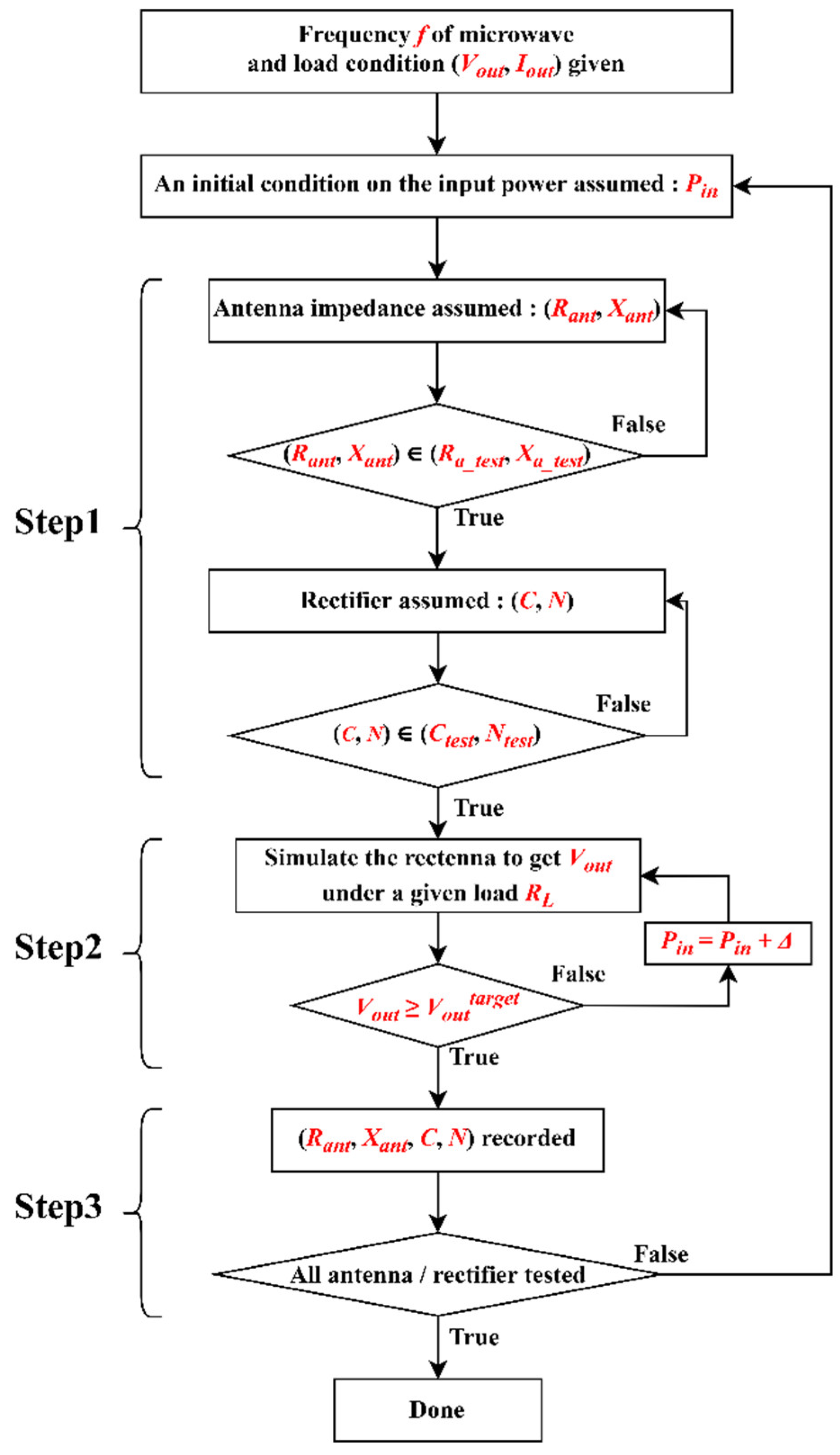
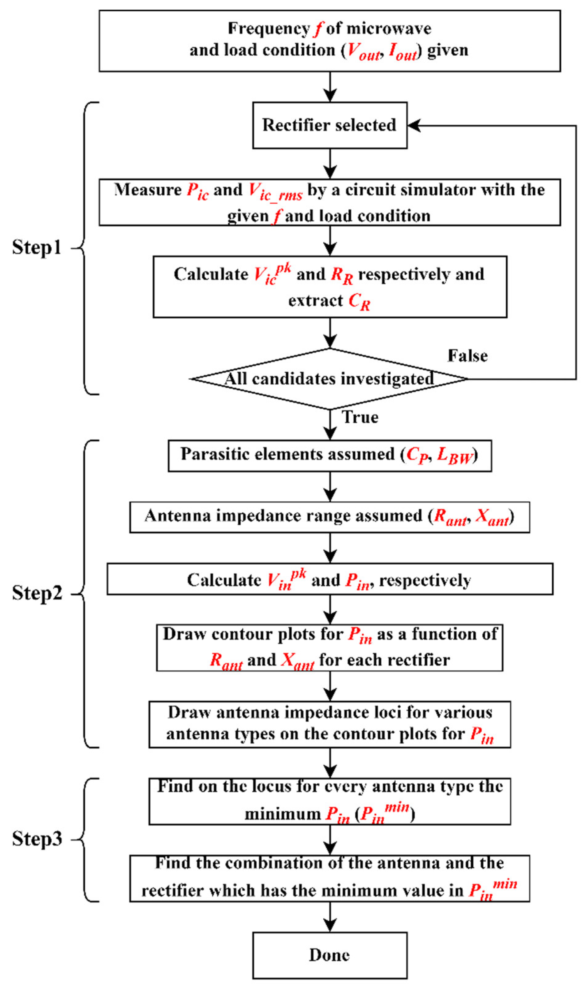
2. Antenna/On-Chip Rectifier Optimum Co-Design Flow
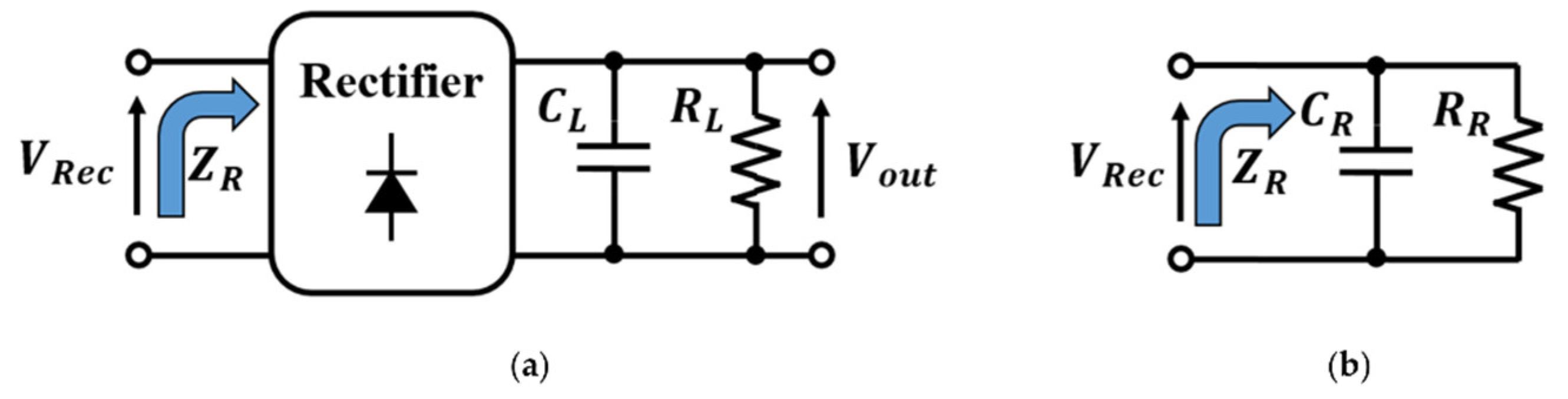
2.1. (Step 1) Determination of and
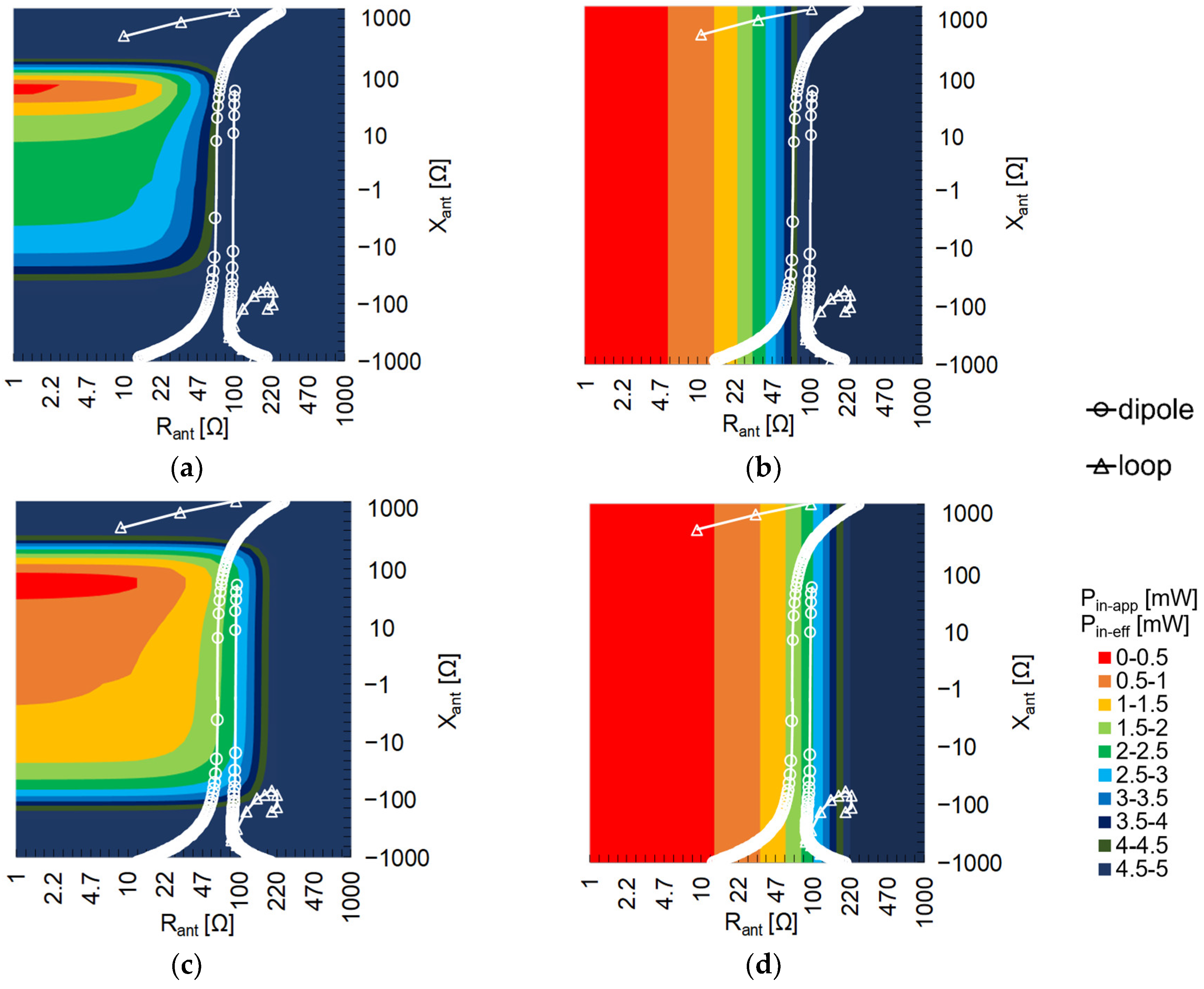
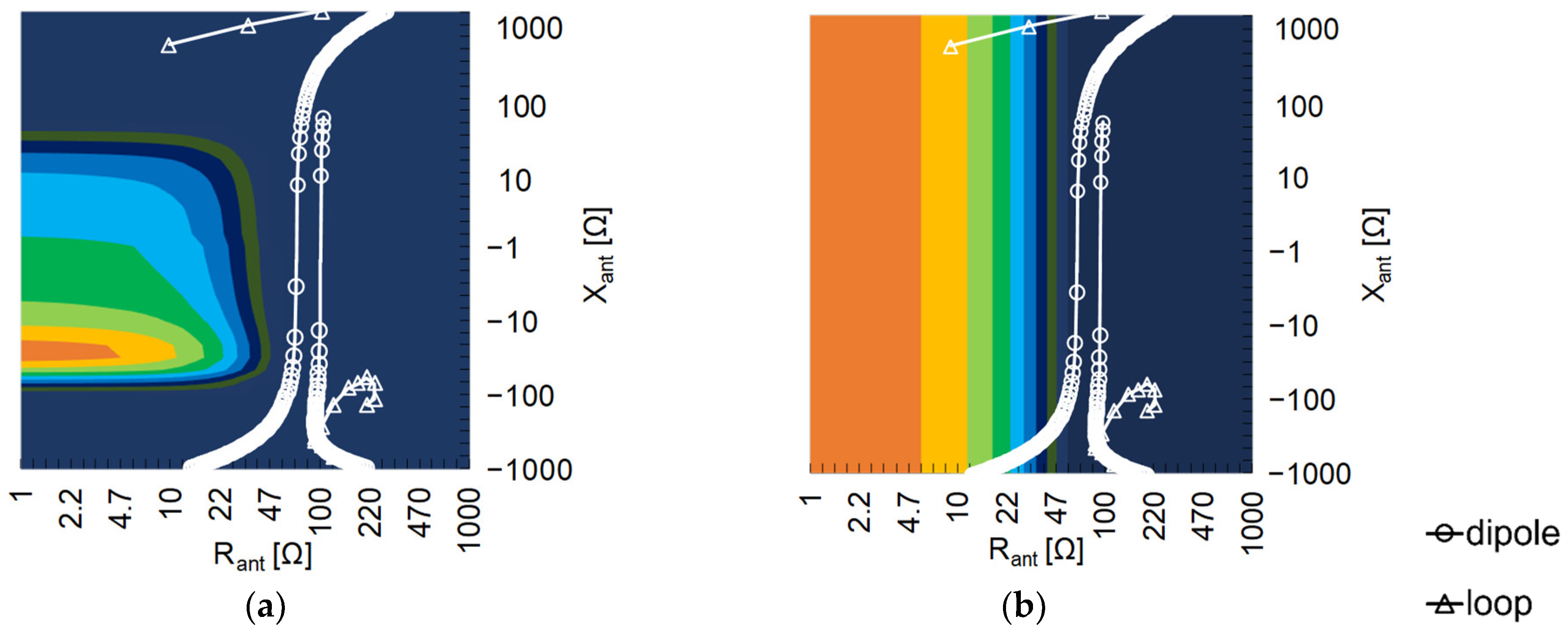
2.2. (Step 2) Drawing Contour Plots of Input Power and Antenna Impedance Loci
- (a)
- Pin with Model 1
- (b)
- Pin with Model 2
2.3. (Step 3) Exploration of Combination of Antenna and Rectifier That Gives Minimum Input Power
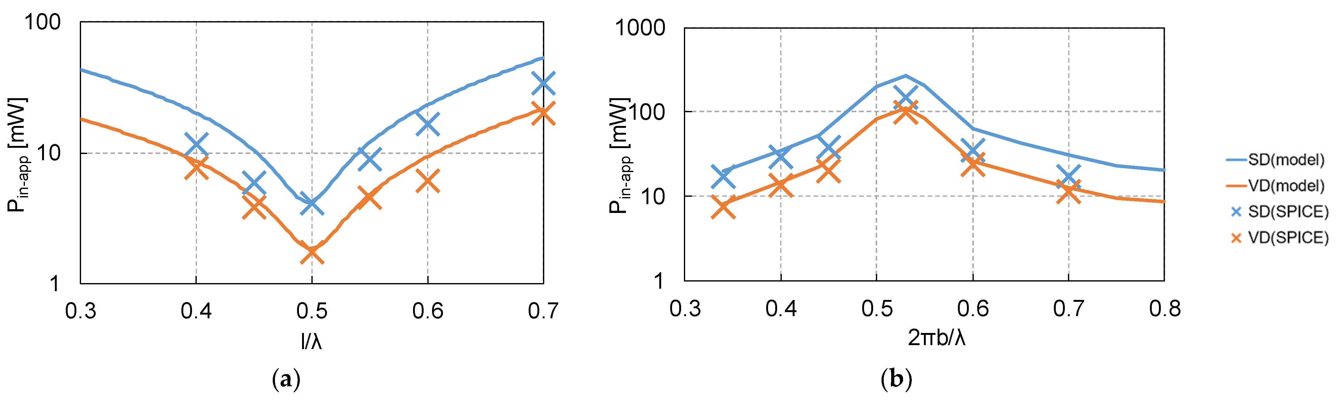
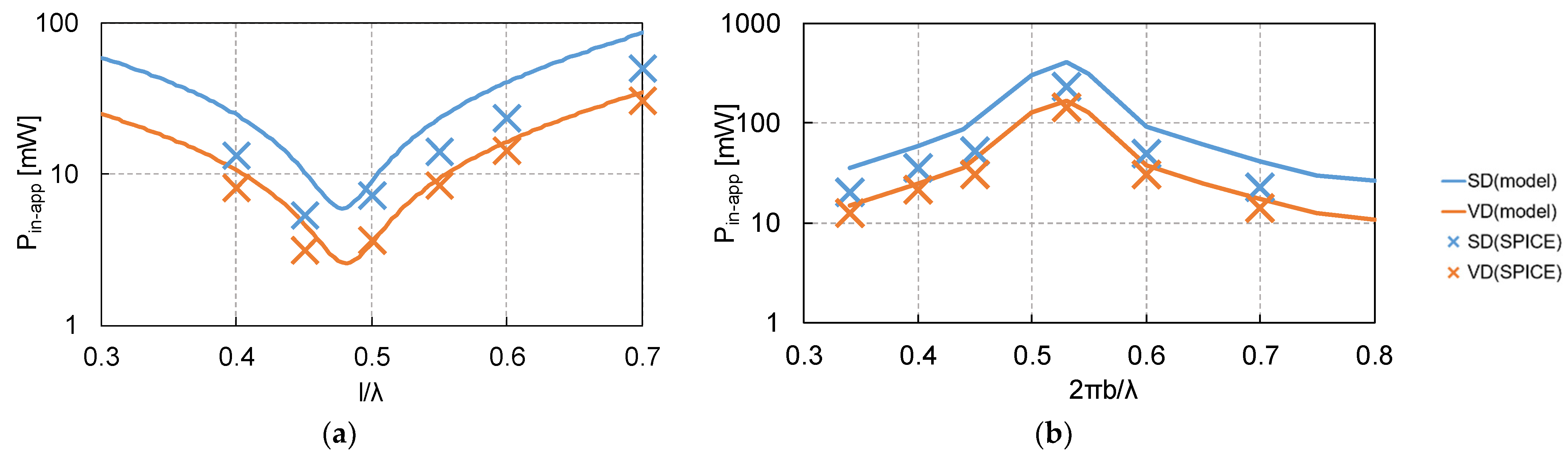
3. Demonstration
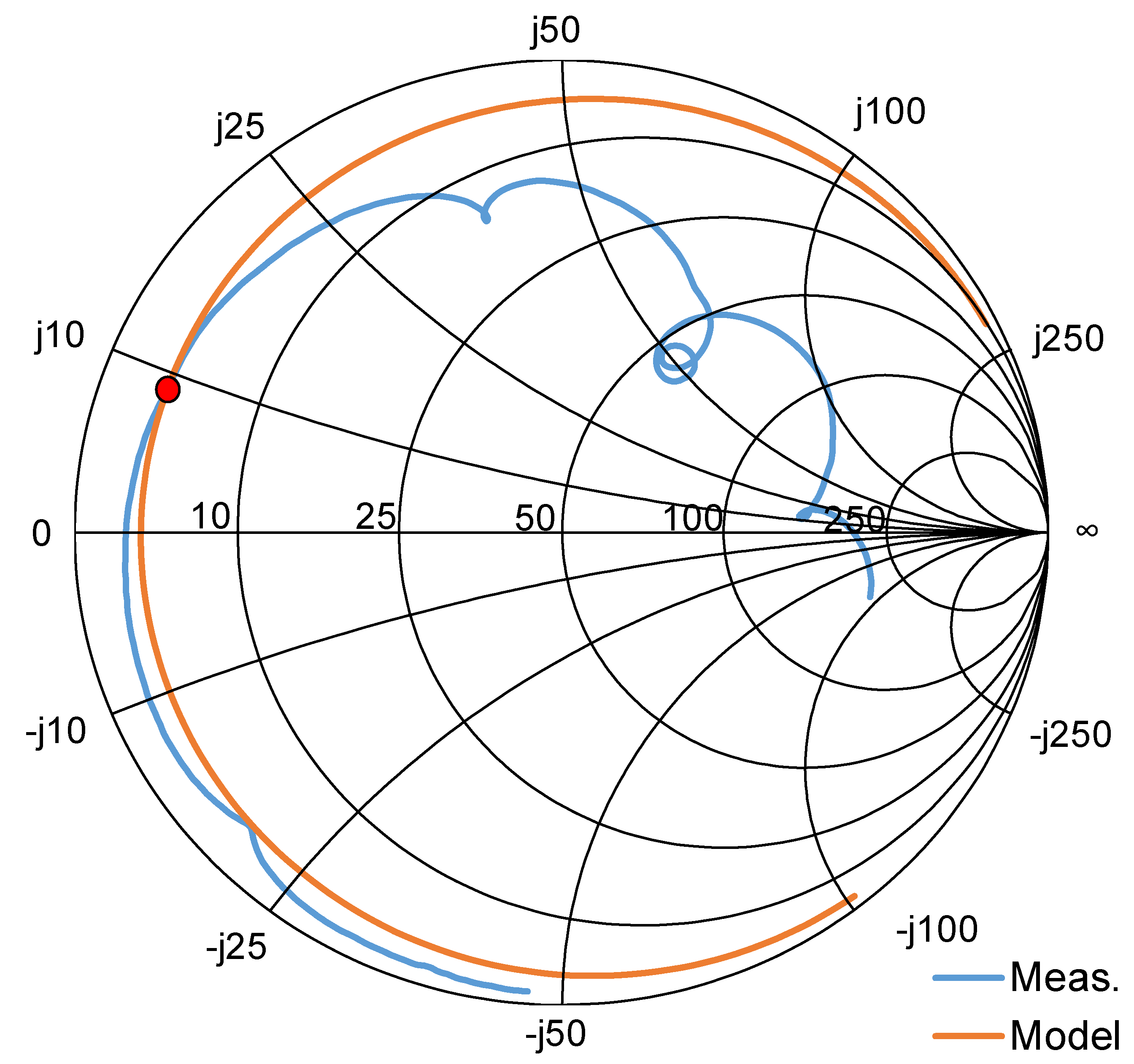
4. Verification of the Proposed Design Flow with Measurement
5. Discussion
- A
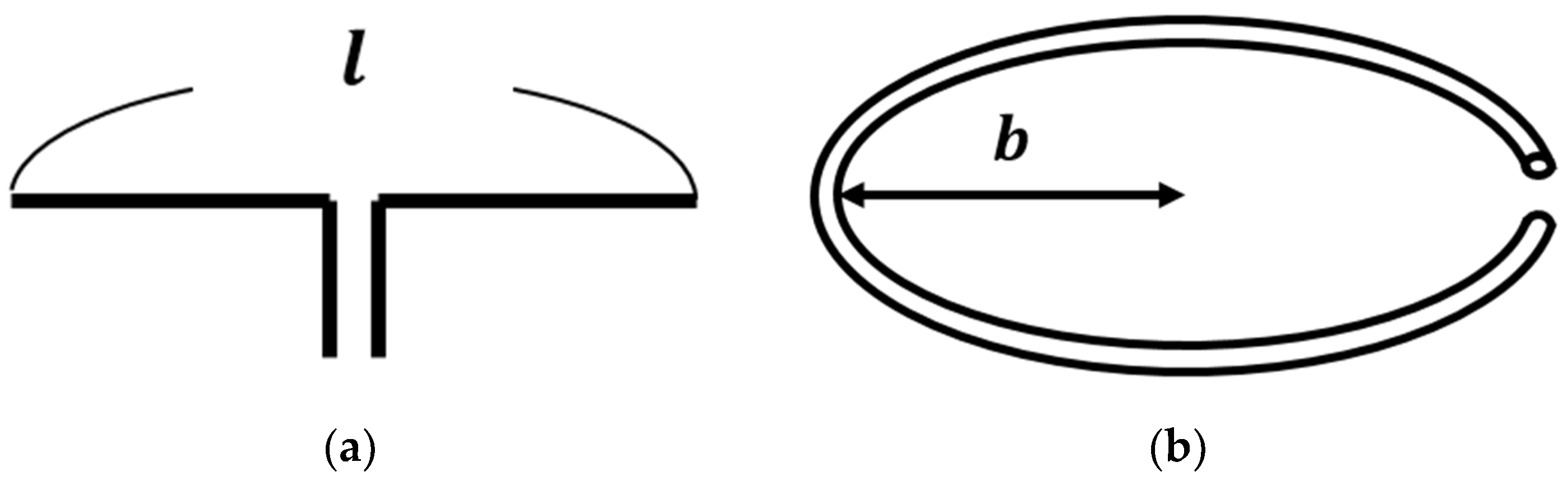
- Antenna impedance
- B
- Relationship between rectifier input impedance and input power
- C
- Limitation of the proposed linearized rectenna model
6. Conclusions
Author Contributions
Funding
Conflicts of Interest
References
- Bi, S.; Ho, C.K.; Zhang, R. Wireless Powered Communication: Opportunities and Challenges. IEEE Commun. Mag. 2015, 53, 117–125. [Google Scholar] [CrossRef]
- Lee, C.; Kim, B.; Kim, J.; Lee, S.; Jeon, T.; Choi, W.; Yang, S.; Ahn, J.-H.; Bae, J.; Chae, Y. A Miniaturized Wireless Neural Implant With Body-Coupled Power Delivery and Data Transmission. IEEE J. Solid-State Circuits, 2022; Early Access. [Google Scholar] [CrossRef]
- Brown, W.C. The history of power transmission by radio waves. IEEE Trans. Microw. Theory Tech. 1984, 32, 1230–1242. [Google Scholar] [CrossRef]
- Gao, H.; Matters-Kammerer, M.K.; Milosevic, D.; van Roermund, A.; Baltus, P. A 62 GHz inductor-peaked rectifier with 7% efficiency. In Proceedings of the 2013 IEEE Radio Frequency Integrated Circuits Symposium (RFIC), Seattle, WA, USA, 2–4 June 2013; pp. 189–192. [Google Scholar] [CrossRef]
- Wu, Z.; Zhao, Y.; Sun, Y.; Min, H.; Yan, N. A Self-Bias Rectifier with 27.6% PCE at −30dBm for RF Energy Harvesting. In Proceedings of the 2021 IEEE International Symposium on Circuits and Systems (ISCAS), Daegu, Korea, 22–28 May 2021; pp. 1–5. [Google Scholar] [CrossRef]
- Mohan, A.; Mondal, S. An Impedance Matching Strategy for Micro-Scale RF Energy Harvesting Systems. IEEE Trans. Circuits Syst. II Express Briefs 2021, 68, 1458–1462. [Google Scholar] [CrossRef]
- Curty, J.-P.; Joehl, N.; Krummenacher, F.; Dehollain, C.; Declercq, M.J. A model for μ-power rectifier analysis and design. IEEE Trans. Circuits Syst. I Regul. Pap. 2005, 52, 2771–2779. [Google Scholar] [CrossRef]
- Gao, H.; Matters-Kammerer, M.K.; Milosevic, D.; van Roermund, A.; Baltus, P. A 50–60 GHz rectifier with −7dBm sensitivity for 1 V DC output voltage and 8% efficiency in 65-nm CMOS. In Proceedings of the 2014 IEEE MTT-S International Microwave Symposium (IMS2014), Tampa, FL, USA, 1–6 July 2014; pp. 1–3. [Google Scholar] [CrossRef]
- Stoopman, M.; Keyrouz, S.; Visser, H.J.; Philips, K.; Serdijn, W.A. Co-Design of a CMOS Rectifier and Small Loop Antenna for Highly Sensitive RF Energy Harvesters. IEEE J. Solid-State Circuits 2014, 49, 622–634. [Google Scholar] [CrossRef]
- Yamazaki, Y.; Tsuchiaki, M.; Tanzawa, T. A Design Window for Device Parameters of Rectifying Diodes in 2.4 GHz Micro-watt RF Energy Harvesting. In Proceedings of the 2019 IEEE Asia-Pacific Microwave Conference (APMC), Singapore, 10–13 December 2019; pp. 135–137. [Google Scholar] [CrossRef]
- Tabuchi, Y.; Tanzawa, T. Rectenna with Serially Connected Diodes for Micro-watt Energy Harvesting. In Proceedings of the 2020 IEEE Wireless Power Transfer Conference (WPTC), Seoul, Korea, 15–19 November 2020; pp. 57–60. [Google Scholar] [CrossRef]
- Miwatashi, K.; Hirakawa, T.; Shinohara, N.; Mitani, T. Development of High-Power Charge Pump Rectifier for Microwave Wireless Power Transmission. IEEE J. Microw. 2022, 2, 711–719. [Google Scholar] [CrossRef]
- Liu, W.; Huang, K.; Wang, T.; Hou, J.; Zhang, Z. A Compact High-Efficiency RF Rectifier With Widen Bandwidth. IEEE Microw. Wirel. Compon. Lett. 2022, 32, 84–87. [Google Scholar] [CrossRef]
- Hashimoto, T.; Tanzawa, T. Antenna/On-Chip-Rectifier Co-Design Methodology for Micro-Watt Microwave Wireless Power Transfer. In Proceedings of the 2022 IEEE 65th International Midwest Symposium on Circuits and Systems (MWSCAS), Fukuoka, Japan, 7–10 August 2022; pp. 1–4. [Google Scholar] [CrossRef]
- Barnett, R.E.; Liu, J.; Lazar, S. A RF to DC Voltage Conversion Model for Multi-Stage Rectifiers in UHF RFID Transponders. IEEE J. Solid-State Circuits 2009, 44, 354–370. [Google Scholar] [CrossRef]
- Oh, S.; Wentzloff, D.D. A −32dBm sensitivity RF power harvester in 130 nm CMOS. In Proceedings of the 2012 IEEE Radio Frequency Integrated Circuits Symposium, Montreal, QC, Canada, 17–19 June 2012; pp. 483–486. [Google Scholar] [CrossRef]
- Balanis, C.A. Antenna Theory Analysis and Design, 3rd ed.; Wiley: New Delhi, India, 2009; pp. 257, 464–466. [Google Scholar]
- Wagih, M.; Weddell, A.S.; Beeby, S. Meshed High-Impedance Matching Network-Free Rectenna Optimized for Additive Manufacturing. IEEE Open J. Antennas Propag. 2020, 1, 615–626. [Google Scholar] [CrossRef]


| Parameter | Description | Parameter | Description |
|---|---|---|---|
| Equivalent input resistance of a rectifier | Parasitic capacitance of a pad | ||
| Equivalent input capacitance of a rectifier | Parasitic inductance of a microstrip line | ||
| Peak input voltage of a rectifier | Parasitic capacitance of a microstrip line | ||
| Real part of the antenna impedance | Parasitic inductance of a bonding wire | ||
| Imaginary part of the antenna impedance | Capacitance of each capacitor | ||
| Number of capacitors |
| Parameters | Value |
|---|---|
| Threshold voltage of transistor | 0.4 |
| Input capacitance of VD | 5.0 |
| 4.3 | |
| 0.5 | |
| 8.0 | |
| 1.3 | |
| 6.0 | |
| 0.2 |
| Rectifier Type | |||
|---|---|---|---|
| SD | 1.4 | 5040 | 31.2 |
| VD | 0.9 | 2060 | 114 |
| Rectifier | (Model 1) | (Model 2) | ||
|---|---|---|---|---|
| SD | 1 + j47 | 0.250 | 1 − j33 | 0.609 |
| VD | 1 + j47 | 0.219 | 1 − j33 | 0.368 |
| Rectifier | ||||
|---|---|---|---|---|
| (Model 1) | (Model 2) | |||
| SD | 4.20 (0.497) | 19.9 (0.34) | 5.95 (0.478) | 26.2 (0.8) |
| VD | 1.85 (0.497) | 8.28 (0.34) | 2.57 (0.478) | 10.9 (0.8) |
Publisher’s Note: MDPI stays neutral with regard to jurisdictional claims in published maps and institutional affiliations. |
© 2022 by the authors. Licensee MDPI, Basel, Switzerland. This article is an open access article distributed under the terms and conditions of the Creative Commons Attribution (CC BY) license (https://creativecommons.org/licenses/by/4.0/).
Share and Cite
Hashimoto, T.; Tanzawa, T. Design Space Exploration of Antenna Impedance and On-Chip Rectifier for Microwave Wireless Power Transfer. Electronics 2022, 11, 3218. https://doi.org/10.3390/electronics11193218
Hashimoto T, Tanzawa T. Design Space Exploration of Antenna Impedance and On-Chip Rectifier for Microwave Wireless Power Transfer. Electronics. 2022; 11(19):3218. https://doi.org/10.3390/electronics11193218
Chicago/Turabian StyleHashimoto, Takuma, and Toru Tanzawa. 2022. "Design Space Exploration of Antenna Impedance and On-Chip Rectifier for Microwave Wireless Power Transfer" Electronics 11, no. 19: 3218. https://doi.org/10.3390/electronics11193218
APA StyleHashimoto, T., & Tanzawa, T. (2022). Design Space Exploration of Antenna Impedance and On-Chip Rectifier for Microwave Wireless Power Transfer. Electronics, 11(19), 3218. https://doi.org/10.3390/electronics11193218