Article

G-Band Broad Bandwidth Extended Interaction Klystron with Traveling-Wave Output Structure

1
Terahertz Science and Technology Key Laboratory of Sichuan Province, School of Electronic Science and Engineering, University of Electronic Science and Technology of China, Chengdu 610054, China
2
No. 55 Research Institute, China Electronics Technology Group Corporation, Nanjing 210016, China
*
Author to whom correspondence should be addressed.
Electronics 2022, 11(19), 3153; https://doi.org/10.3390/electronics11193153
Submission received: 29 August 2022 / Revised: 27 September 2022 / Accepted: 27 September 2022 / Published: 30 September 2022

Abstract

:
In this paper, we investigate a large-sized beam tunnel, G-band extended interaction klystron (EIK) with a traveling wave output structure for the development of broad bandwidth EIKs. The high-quality factor F was introduced to estimate the bandwidth characteristics of the cluster cavities, and the optimal cluster cavity structure parameters were obtained based on this factor. The simulation mode of the device was designed by the 3D particle-in-cell (PIC) commercial simulation software. Four cluster cavities with a staggered distribution of frequencies were employed to expand the bunching bandwidth, and two traveling wave modes, 2π−π/10 and 2π−2π/10, were used as the operating modes in the output structure, effectively increasing the output bandwidth. The simulation findings show that the maximum output power is 170 W, the corresponding gain is 37.5 dB, and the 3-dB bandwidth is up to 1.25 GHz. The three-hole coupling structure with a large-sized beam tunnel provides convenience for the fabrication of devices in the G-band, and our study shows a potential method for the realization of a G-band broadband EIK.

1. Introduction

A vacuum electronic device (VED) includes oscillators [1,2,3] and amplifiers; due to the high output power and broad bandwidth [4,5,6], vacuum electronic amplifiers (VEAs) have been successfully and widely applied for the purposes of radar, satellite communications, security checks, and medical diagnoses [7,8,9]. Traveling-wave tubes (TWTs) and klystrons are the two main kinds of VEAs. TWTs have the broadest bandwidth among the VEAs, and are widely used in many fields. However, with the further increase in operating frequency, especially in the millimetre wave and terahertz bands, the power loss is dramatically enhanced, which results from a longer slow-wave structure and smaller beam tunnel in TWTs, raising the processing difficulty and cost of the device. The inherent advantage of the extended interaction klystron (EIK) is that it can simultaneously possess high output power and high gain. However, compared with TWTs, EIKs are a kind of relatively narrowband device [10,11,12,13].
After decades of development, some achievements have been made in the research of EIKs. Ka-band and G-band EIKs have been successfully produced by CPI Canada; the EIK of the Ka-band can produce 1 kW of continuous output power with the 1-dB bandwidth measured at 500 MHz [14], and the EIK of the G-band can produce 7 W of output power with the 3-dB bandwidth measured at 300 MHz [15]. An EIK designed by the United States Naval Research Laboratory is capable of producing 453 W of power with a gain of 41.6 dB in the Ka-band [16]; they have also produced a G-band EIK with a 7.5 kW power output with a bandwidth of 100 MHz [17]. A W-band EIK produced by the Beijing Vacuum Electronics Research Institute can produce a power output of 5.6 W, and the 3-dB bandwidth is 100 MHz [18].
Although the research surrounding EIKs has made great achievements, the requirement of broader bandwidths limits the further application of EIKs. The bandwidth of an EIK is determined by both the output and bunching bandwidth. Generally, the bunching bandwidth can be expanded by increasing the number of cluster cavities and staggering the tune of each cavity frequency. The output bandwidth can be improved through the adoption of a traveling-wave output circuit, overlapping mode operation, or filter loads in the output circuit [19].
In order to develop a broad bandwidth EIK, we studied a G-band broad bandwidth EIK in this paper that is based on the traveling-wave output structure. A three-hole coupling cavity structure has been proposed and used as the beam-wave interaction structure, and the unique large-sized beam tunnel reduces the difficulty of designing and fabricating an electron-optical system. Meanwhile, the large-sized beam tunnel is capable of transmitting a high operating current, which provides a sound basis for realizing a high output power device. Comparing other works [20,21], the resonant cavity of the device in this paper is of uniform periodic structure, and the thickness of the disk of the three-hole coupling cavity is greater than 0.2 mm; this makes it easier to control the precision in the machining of our structure, as well as making it easier to realize in engineering terms. The high-frequency structure consists of five cavities, and the frequency of each cavity are staggered around the center frequency. The output cavity operates in a traveling-wave mode in order to expand the output bandwidth. With this structure, we have realized a G-band EIK based on the three-coupling hole structure with a broad bandwidth of >1.2 GHz at an output power of >150 W.

2. Design and Simulation of the Beam-Wave Interaction Structure

In this section, the process of the structural design and parameter optimization of the G-band broad bandwidth EIK based on a three-hole coupling cavity structure is described by the simulation software. Figure 1 shows the schematic of the three-hole coupling cavity and disk in the simulation. The fan-shaped coupling holes are located at the edge of the disk and are evenly distributed. The angle and height of the coupling hole can be optimized to obtain an appropriate frequency, bandwidth, and effective characteristic impedance.

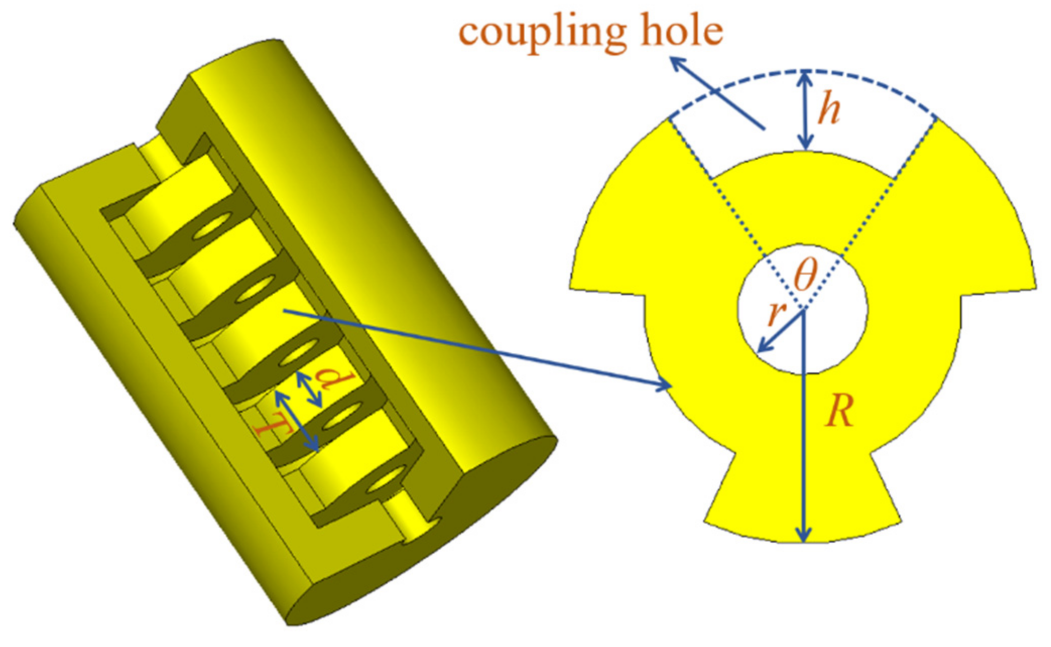
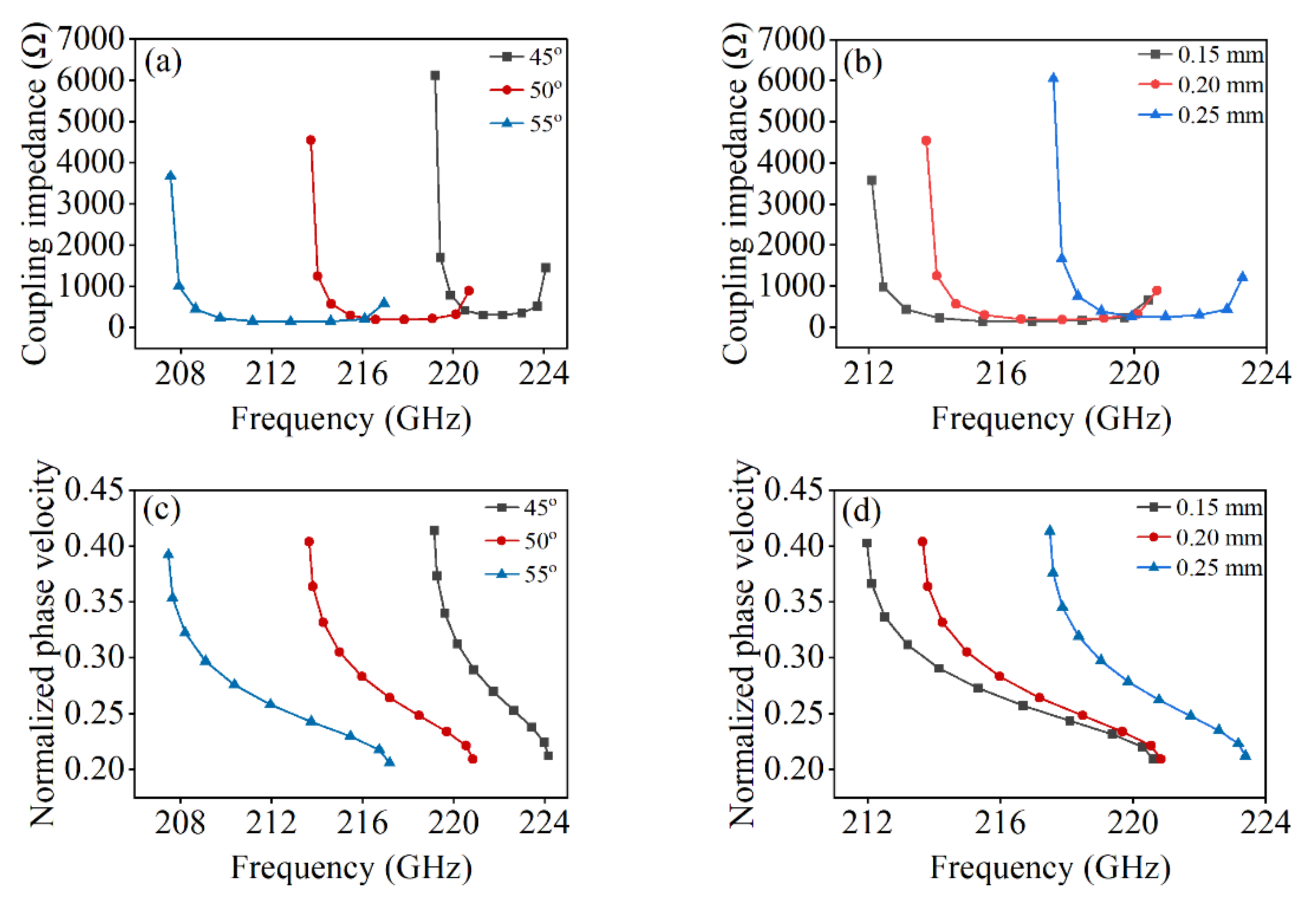
2.1. Cluster Cavities Design

Here, the effective characteristic impedance (R/QM2 was adopted to evaluate the ability of beam-wave interaction. R/Q and M are the characteristic impedance and coupling coefficient, respectively, which are expressed as [22]:
R Q = ( E Z d z ) 2 2 ω W s
M = E z e j β e z d z E z d z
where Ez is the axis electric field, and Ws and ω are the total stored energy and radian frequency, respectively. In this work, the TM01-2π mode is set as the operating mode in the cluster cavities. For the cluster cavity, where bandwidth is related to the conductance Ge [19,23], we introduce the high-quality factor F to evaluate the bandwidth characteristics of the cluster cavities, defined as [19]:
F = M 2 ( R Q ) ( G e G 0 ) G 0
Here, Ge/G0 is the normalized beam conductance, calculated from:
G e G 0 = 1 8   β e β q [ | M ( β e β q ) | 2 | M ( β e + β q ) | 2 ]
The direct current conductance G0 is expressed as the operating current divided by the operating voltage; the coupling coefficient M(βeβq) of the fast space-charge wave and the coupling coefficient M(βe + βq) of the slow space-charge waves can be calculated from Equation (2). The wave constant βe and plasma reduction phase constant βq can be calculated from:
β e = ω 0 u 0
β q = ω q u 0
u 0 = c · 1 1 ( 1 + V 511 k V ) 2
where ω0, ωq, u0, and c are the radian frequency, reduced plasma radian frequency, electron velocity, and speed of light, respectively. V is the operating voltage (unit: kV).
For the cluster cavities, we expected to obtain the maximum value of M2(R/Q)(Ge/G0) in order to expand the bunching bandwidth. Therefore, according to previous experience [24], the sensitive geometric parameters d, h, and θ of the cavity were analysed for the influence of M2(R/Q)(Ge/G0); here, d is the thickness of disk and h and θ are the height and angle of the coupling hole, respectively.
As shown in the Figure 2a, the value of M2(R/Q)(Ge/G0) increases and then decreases when the value of d increases, and a maximum value of 7.2 Ω is obtained when the value of d is 0.22 mm. Figure 2b shows the variation trend of M2(R/Q)(Ge/G0) with h. In general, the value of M2(R/Q)(Ge/G0) increases as h increases; however, if a large value of h is used in engineering practice, the lateral thickness of the disk will be too thin and is easily damaged. Here, the value of h was selected as 0.2 mm. In Figure 2c, when the value of θ is 50°, a maximum value M2(R/Q)(Ge/G0) of about 4.5 Ω appears.
Based on the above analysis and a fine-tuning of parameter d to optimize the frequency distribution of each cavity, the finally determined geometric parameters of each cavity are listed in the Table 1. The beam tunnel radius is 0.13 mm, and in the engineering practice, an industrial microscope was used for device alignment. Using the eigenmode simulation of the CST in combination with numerical calculation, the optimal cold cavity parameters were obtained and are listed in the Table 2. f is the cavity frequency and Q0 and Qe are the unloaded and external quality factors. In order to expand the bunching bandwidth, the frequency of the first intermediate cavity was set below the frequency of the input cavity, and the frequency difference was 550 MHz; the frequency of the second intermediate cavity was set above the frequency of the input cavity, leading to a frequency difference of 670 MHz. The frequency of the third intermediate cavity was set above the frequency of the second intermediate cavity, leading to a frequency difference of 360 MHz. The Qe of the input cavity was selected to be the smaller value of 176.

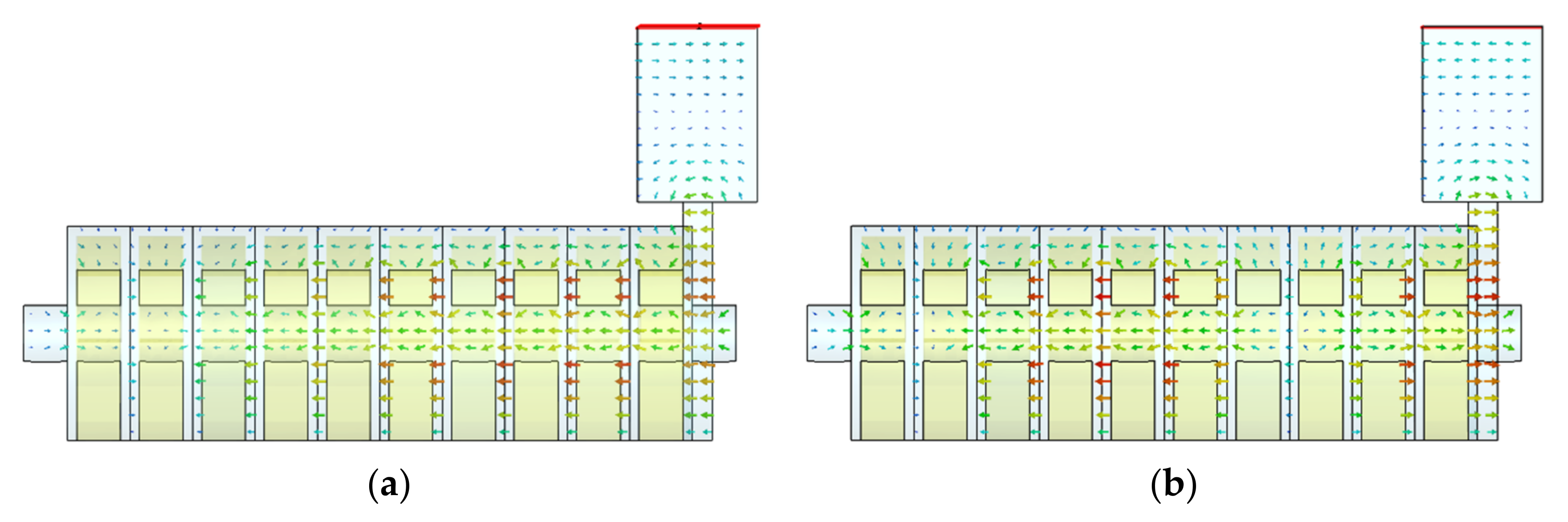
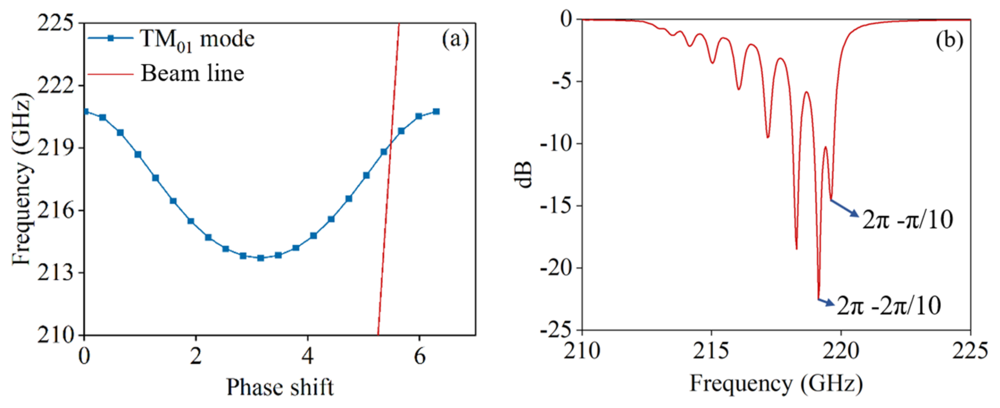
2.2. Traveling Wave Output Structure Design

In this work, the output slow-wave structure, the ten gap, operated at the traveling wave modes of 2π−π/10 and 2π−2π/10. As shown in the Figure 3a and b, the phase of the electric field changes once and twice, respectively. The parameters h and θ were optimized by using CST Microwave Studio to improve the coupling impedance and dispersion, which are essential to the slow-wave structure to evaluate the beam-wave interaction efficiency and bandwidth. Figure 4 shows the variation trend of the coupling impedance and the normalized phase velocity with different coupling hole angles and heights, indicating that when the coupling hole angle θ decreases or the coupling hole height h increases, the coupling impedance will accordingly increase. However, the dispersion curve will become increasingly steep, which is not conducive to the improvement of the bandwidth. After a comprehensive consideration, the values of h and θ were selected to be 0.2 mm and 50°, respectively. Finally, the dispersion curve of the TM01 mode and electron beam are shown in the Figure 5a; the beam voltage is slightly higher than the synchronous voltage of the two operating modes and is more beneficial to the beam-wave interaction.
The output structure set at the end of the traveling-wave output structure consists of a transitional waveguide connected to a standard waveguide. The reflection parameter S11 of the structure was calculated, as shown in the Figure 5b.

3. PIC Simulation Results

The 3D simulation model of the five cavity G-band EIK is shown in the Figure 6. The input cavity and three intermediate cavities are the resonant cavities of the five gaps, and the output structure has ten periods. Considering the power loss of the G-band in engineering practice, the material was set as oxygen-free copper with a conductivity of 2.36 × 10⁷ S/m in the simulation [25], and the operating voltage and current were set to 15.2 kV and 0.3 A, respectively. The beam radius was 0.12 mm with a constant focusing magnetic field of 1 Tesla [24].
The electron phase-space diagram of the beam energy is shown in Figure 7a, which depicts the energy exchange process of the beam-wave interaction. The electron beam is gradually modulated by the input cavity and intermediate cavities, and then a well-modulated electron beam interacts with the high frequency field and releases energy in the output slow-wave structure. Figure 7b shows the final results of the beam-wave interaction. The output power was 170 W with an input power of 30 mW, and the corresponding gain is 37.5 dB; in the long simulation time of 50 ns, the output power is stable, the spectrum of the output signal is pure at a wide frequency range, and it is consistent with the input signal. This indicates that the system is stable and self-oscillations have not occurred.
Figure 8 shows the output power and gain versus the frequency. A maximum output power and gain appeared at the frequency of 219.2 GHz. The 3-dB bandwidth reached 1.25 GHz.

4. Conclusions

In this paper, we investigated a five cavity G-band broad bandwidth EIK with a large-sized beam tunnel based on the three-hole coupling structure. For the cluster cavities, the high-quality factor F has been introduced and analysed, and we have tuned each cavity frequency and distributed it in a stagger around the center frequency. Meanwhile, a traveling-wave slow-wave structure has been used as the output cavity to expand the output bandwidth, and the coupling hole parameters have been analysed for the influence of the coupling impedance and dispersion. Simulation results demonstrate the purity of the output signal spectrum and stability of the system. A maximum output power of 170 W was obtained with the gain of 37.5 dB, and the 3-dB bandwidth was extended to 1.25 GHz. Compare with the traveling-wave tube, the EIK with a traveling-wave output structure shows a great advantage in output power and gain, and has a shorter longitudinal length similar to the device in [26,27]. The output power of the TWTs is about 50 W, but the length of the slow-wave structure is more than 80 mm. Meanwhile, there is a great potential for the improvement of bandwidth in EIKs as demonstrated by our device, and it lays important foundations for the development of a new generation of VEAs.

Author Contributions

Conceptualization, methodology, idea proposal, writing, and result, X.X. and X.Y.; conceptualization, draft preparation, editing, and visualization, H.L. (Hengliang Li), Q.C. and Y.Z.; conceptualization and reviewing, H.L. (Hailong Li) and Y.Y. (Yong Yin); draft preparation, editing, and reviewing, Y.Y. (Yang Yan). All authors have read and agreed to the published version of the manuscript.

Funding

This research was funded by the National Key Research and Development Program of China, Grant No. 2019YFA0210202; Sichuan Science and Technology Program, Grant No. 2021YJ0096; National Natural Science Foundation of China, Grant No. 61771096; and Fundamental Research Funds for the Central Universities, Grant No. ZYGX2019J012.

Conflicts of Interest

The authors declare no conflict of interest.

References

  1. Mumtaz, S.; Choi, E.H. An efficient vircator with high output power and less drifting electron loss by forming multi virtual cathodes. IEEE Electron. Device Lett. 2022, 43, 1756–1759. [Google Scholar] [CrossRef]
  2. Mumtaz, S.; Uhm, H.; Lim, J.S.; Choi, E.H. Output-Power Enhancement of Vircator Based on Second Virtual Cathode Formed by Wall Charge on a Dielectric Reflector. IEEE Trans. Electron. Devices 2022, 69, 2043–2050. [Google Scholar] [CrossRef]
  3. Dubinov, A.E.; Saikov, S.K.; Tarakanov, V.P. Multivircator as a New Highly Effective Microwave Generator with Multiple Virtual Cathodes: Concept and PIC-Simulation. IEEE Trans. Plasma Sci. 2020, 48, 141–145. [Google Scholar] [CrossRef]
  4. Booske, J.H.; Dobbs, R.J.; Joye, C.D.; Kory, C.L.; Neil, G.R.; Park, G.-S.; Park, J.; Temkin, R.J. Vacuum Electronic High Power Terahertz Sources. IEEE Trans. Terahertz Sci. Technol. 2011, 1, 54–75. [Google Scholar] [CrossRef]
  5. Ulisse, G.; Krozer, V. W-Band Traveling Wave Tube Amplifier Based on Planar Slow Wave Structure. IEEE Electron. Device Lett. 2017, 38, 126–129. [Google Scholar] [CrossRef]
  6. Shin, Y.M.; Wang, J.X.; Barnett, L.R.; Luhmann, N.C. Particle-In-Cell Simulation Analysis of a Multicavity W-Band Sheet Beam Klystron. IEEE Trans. Electron. Devices 2011, 58, 251–258. [Google Scholar] [CrossRef]
  7. Carr, G.L.; Martin, M.C.; Mckinney, W.R.; Jordan, K.; Neil, G.; Williams, G. Very high Power THz radiation from Relativistic Electrons. In Proceedings of the Twenty Seventh International Conference on Infrared and Millimeter Waves, San Diego, CA, USA, 26 September 2002; Volume 420, pp. 153–156. [Google Scholar]
  8. Liu, W.; Zhang, Z.; Zhao, C.; Guo, X.; Zhang, Z.; Liao, S. Development of a Subterahertz Folded-Waveguide Extended Interaction Oscillator. IEEE Trans. Plasma Sci. 2017, 45, 1731–1738. [Google Scholar] [CrossRef]
  9. Li, R.; Ruan, C.; Zhang, H.; Fahad, A.K.; Shan, S.; He, Y. Optimization and improvement of output performance in G-band extended interaction klystron. J. Infrared Millim. Terahertz Waves 2018, 40, 5–16. [Google Scholar] [CrossRef]
  10. Zhang, C.Q.; Ruan, C.J.; Wang, S.Z.; Yang, X.Y. High-power extended-interaction klystron with ladder-type structure. J. Infrared Millim. Waves 2015, 34, 307–313. [Google Scholar]
  11. Li, S.; Ruan, C.; Fahad, A.K.; Wang, P.; Zhang, Z.; He, W. Novel Coupling Cavities for Improving the Performance of G-Band Ladder-Type Multigap Extended Interaction Klystrons. IEEE Trans. Plasma Sci. 2020, 48, 1350–1356. [Google Scholar] [CrossRef]
  12. Chernin, D.; Burke, A.; Chernyavskiy, I.; Petillo, J.; Dobbs, R.; Roitman, A.; Horoyski, P.; Hyttinen, M.; Berry, D.; Blank, M.; et al. Extended Interaction Klystrons for terahertz power amplifiers. In Proceedings of the 2010 IEEE International Vacuum Electronics Conference, Monterey, CA, USA, 18–20 May 2010. [Google Scholar]
  13. Chodorow, M.; Wessel-Berg, T. A High-Efficiency Klystron with Distributed Interaction. IRE Trans. Electron. Devices 1961, 8, 44–55. [Google Scholar] [CrossRef]
  14. Harvey, W.; Tope, M.; Esteban-Fernandez, D.; Roitman, A.; Sokol, E.; Berry, D. Development path of a Ka-Band Extended Interaction Klystron for space-borne interferometer. In Proceedings of the 2016 IEEE International Vacuum Electronics Conference, Monterey, CA, USA, 19–21 April 2016. [Google Scholar]
  15. Roitman, A.; Horoyski, P.; Hyttinen, M.; Roitman, A.; Steer, B. Extended Interaction Klystrons for Submillimeter Applications. In Proceedings of the 2006 IEEE International Vacuum Electronics Conference held Jointly with 2006 IEEE International Vacuum Electron Sources, Monterey, CA, USA, 25–27 April 2006. [Google Scholar]
  16. Nguyen, K.T.; Pasour, J.; Wright, E.L.; Pershing, D.E.; Levush, B. Design of a G-band sheet-beam Extended-Interaction Klystron. In Proceedings of the 2009 IEEE International Vacuum Electronics Conference, Rome, Italy, 28–30 April 2009. [Google Scholar]
  17. Pasour, J.; Wright, E.; Nguyen, K.T.; Balkcum, A.; Wood, F.N.; Myers, R.E.; Levush, B. Demonstration of a Multikilowatt, Solenoidally Focused Sheet Beam Amplifier at 94 GHz. IEEE Trans. Electron. Devices 2014, 61, 1630–1636. [Google Scholar] [CrossRef]
  18. Zeng, Z.; Zhou, L.; Li, W.; Chen, H. Design and optimization of a W-band extended interaction klystron amplifier. In Proceedings of the 2015 IEEE International Vacuum Electronics Conference (IVEC), Beijing, China, 27–29 April 2015. [Google Scholar]
  19. Ding, Y.G. Design, Manufacture and Application of High Power Klystron; National Defense Industry: Beijing, China, 2010; pp. 61–68. [Google Scholar]
  20. Li, R.; Ruan, C.; Zhang, H.; Haq, T.U.; He, Y.; Shan, S. Theoretical Design and Numerical Simulation of Beam-Wave Interaction for G-Band Unequal-Length Slots EIK with Rectangular Electron Beam. IEEE Trans. Electron. Devices 2018, 65, 3500–3506. [Google Scholar] [CrossRef]
  21. Zhang, F.; Zhao, Y.; Ruan, C. A High-Power and Broadband G-Band Extended Interaction Klystron Based on Mode Overlap. IEEE Trans. Electron. Devices 2022, 69, 4611–4616. [Google Scholar] [CrossRef]
  22. Ding, Y.G. Theory and Computer Simulation of High Power Klystron; National Defense Industry Press: Beijing, China, 2008; pp. 44–47. [Google Scholar]
  23. Ding, Y.G.; Niu, X.H.; Li, D.K. A S-band 2.5 MW high-power broadband klystron. J. Electron. Inf. Technol. 1985, 7, 247–253. [Google Scholar]
  24. Xu, X.; Yuan, X.; Li, H.; Chen, Q.; Zu, Y.; Cole, M.; Xie, J.; Yin, Y.; Yan, Y. Design of a G-Band Extended Interaction Klystron Based on a Three-Coupling-Hole Structure. IEEE Trans. Electron. Devices 2022, 69, 1368–1373. [Google Scholar] [CrossRef]
  25. Ao, X.; Linlin, H.; Lei, Y. Design and machining of components of 0.22 THz folded waveguide traveling wave tube. Qiangjiguang Yu Lizishu 2012, 24, 2135–2140. [Google Scholar]
  26. Zhang, L.; Wei, Y.; Guo, G.; Ding, C.; Wang, Y.; Jiang, X.; Zhao, G.; Xu, J.; Wang, W.; Gong, Y. A Ridge-Loaded Sine Waveguide for G-Band Traveling-Wave Tube. IEEE Trans. Plasma Sci. 2016, 44, 2832–2837. [Google Scholar] [CrossRef]
  27. Nayek, N.; Joshi, M.K.; Sonkar, R.K.; Tiwari, T.; Bhattacharjee, R. Design and Analysis of Width-Modulated Two-Section Sine Waveguide for G-Band Traveling-Wave Tube. IEEE Trans. Electron. Devices 2021, 68, 6458–6464. [Google Scholar] [CrossRef]
Figure 1. Schematic of the three-hole coupling cavity and disk in the simulation.
Electronics 11 03153 g001
Figure 2. (ac) M2(R/Q)(Ge/G0) as functions of d, h, and θ, respectively.
Electronics 11 03153 g002
Figure 3. (a) E-field distribution of the TM01-(2π−π/10) mode. (b) E-field distribution of the TM01-(2π−2π/10) mode.
Electronics 11 03153 g003
Figure 4. (a) The coupling impedance as a function of coupling hole angle when h is 0.2 mm. (b) The coupling impedance as a function of coupling hole height when θ is 50°. (c) The normalized phase velocity of the coupling hole with different angles when h is 0.2 mm. (d) The normalized phase velocity of the coupling hole with different heights when θ is 50°.
Electronics 11 03153 g004
Figure 5. (a) The dispersion curve of the TM01 mode and electron beam; the frequency of the intersection is slightly lower than the frequency of the 2π−2π/10 mode. (b) The reflection parameter S11 of the traveling wave output structure; the curve of the segment near 2π−π/10 mode and 2π−2π/10 mode is less than −10 dB.
Electronics 11 03153 g005
Figure 6. 3D PIC simulation model of the complete circuit.
Electronics 11 03153 g006
Figure 7. (a) The phase-space diagram of the electron beam energy, where it is shown that the electron beam is well-modulated in each cavity. (b) Output power versus time. Inset: frequency spectra of the input and output signals. It is shown that the spectrum is pure, and the frequency of the output signal is exactly the same as that of the input signal.
Electronics 11 03153 g007
Figure 8. The output power and gain versus the frequency.
Electronics 11 03153 g008
Table 1. Geometric parameters of each cavity.
Input CavityIntermediate Cavity 1Intermediate Cavity 2Intermediate Cavity 3Output Structure
h (mm)0.20.20.20.20.2
θ50°50°50°50°50°
d (mm)0.2160.220.2170.2190.2
R (mm)0.4940.4940.4920.4910.49
T (mm)0.320.320.320.320.285
r (mm)0.13
Table 2. Cavity parameters.
Input CavityIntermediate Cavity 1Intermediate Cavity 2Intermediate Cavity 3
f (GHz)219.7219.15220.37220.73
Q0750421433418
Qe176
M2(R/Q)(Ge/G0) (Ω)2.27.26.96.9
Publisher’s Note: MDPI stays neutral with regard to jurisdictional claims in published maps and institutional affiliations.

