1. Introduction
Infrared (IR) cameras, which detect objects with infrared radiation instead of visible light, are widely used in various fields [
1]. In particular, the demand for compact and power-efficient portable infrared cameras has increased for use in ultralight portable devices, such as drones or head-mounted displays (HMDs). A cooled IR camera lowers the sensor temperature to cryogenic temperatures, which is necessary to reduce thermally induced noise. However, cryogenic cooling systems consume high power and occupy a large volume. Therefore, considerable research has been conducted on microbolometers, which are uncooled infrared sensors that do not require cryogenic cooling systems [
2,
3,
4,
5]. The microbolometer is a representative thermal infrared sensor that uses a heat-sensitive material whose resistance changes with temperature. Amorphous silicon (a-Si), thin-film vanadium oxide (VO
x), and titanium oxide (TiO
x) are widely used as heat-sensitive materials.
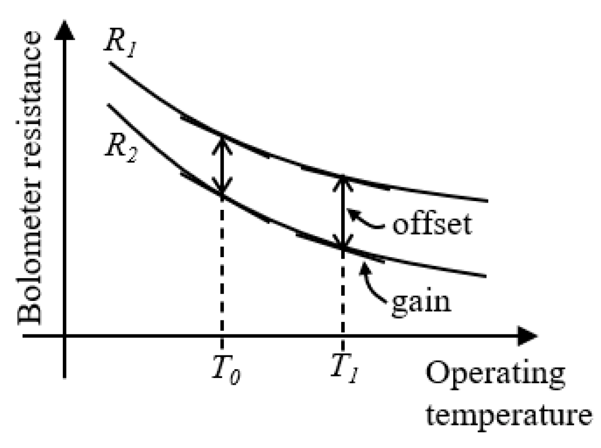
Since two-dimensional microbolometer arrays have large variations in characteristics between pixels, non-uniformity correction is essential for excellent infrared images [
6]. However, the uniformity of a microbolometer array is highly sensitive to changes in operating temperature.
Figure 1 shows the variation in resistance with temperature for two bolometers. As the change in bolometer resistance according to the operating temperature is highly nonlinear, the offset and gain differences between the two bolometers vary according to the operating temperature. To solve this problem, a thermoelectric cooler (TEC) can be used to maintain the bolometer array at a constant operating temperature. However, because TECs consume high power and occupy a large volume, they cannot be used for applications in ultralight portable devices [
7,
8].
Because of the well-established silicon manufacturing methods and the simplicity of its structure, the a-Si-based microbolometer array exhibits uniform characteristics [
9]. Therefore, good uniformity can be maintained without a TEC by simply adjusting the offset correction coefficient according to the operating temperature [
10]. VO
x and TiO
x microbolometers show superior 1/f noise compared with a-Si microbolometers. However, they show a relatively higher non-uniformity because metal oxides have various phases, and their characteristics change with time due to high bias current. Therefore, good uniformity cannot be obtained only by adjusting the offset correction coefficient for VO
x or TiO
x microbolometers. The adjustment of the gain correction coefficient is additionally required according to the operating temperature [
11]. Calibration for each sensor can be performed without a TEC using linear interpolation to adjust the gain and offset correction coefficients according to the current operating temperature [
1]. However, there is an additional cost to find a table of correction coefficients for the operating temperature point. Moreover, time-varying characteristics cannot be calibrated.
In this study, we propose a novel readout integrated circuit (ROIC) with a simple structure capable of efficient non-uniformity correction (NUC) over a wide operating temperature range without using a TEC. Offset and gain can be corrected in real time and even the ‘aging’ phenomenon, in which characteristics change over time, can be corrected. In addition, the use of a pixel-level analog-to-digital converter (ADC) enables fast and accurate correction according to the surrounding environment.
3. Proposed ROIC for Real-Time NUC without a TEC
3.1. Circuit Operation for Calibration in the Production
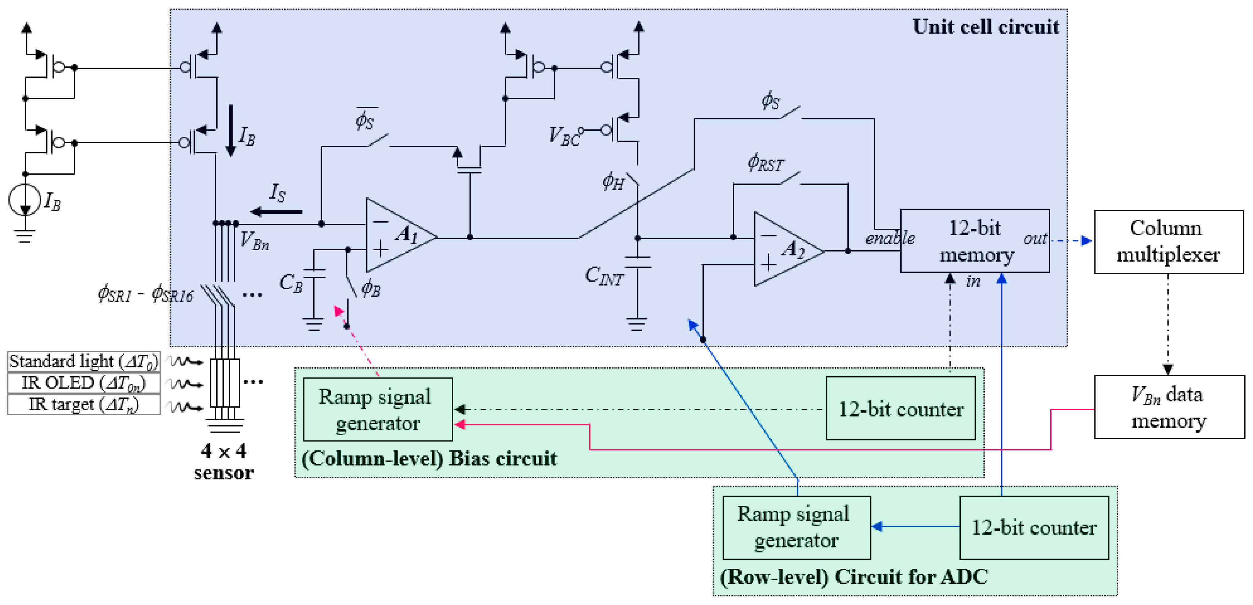
Figure 4 and
Figure 5 show the schematic of the unit cell circuit and block diagram of the overall arrangement for the proposed ROIC, respectively. As the pixel size (17 μm × 17 μm) of the sensor is very small, it is difficult to implement the unit cell circuit shown in
Figure 4 within one pixel. Accordingly, 16 (4 × 4) adjacent bolometers used as IR sensors share one unit cell circuit using 16 switches (
ϕSR1 −
ϕSR16) in a time-division manner. The bolometer resistance
RB at temperature
T is given by the following equation:
where
Ro and
b are constants that are determined by the physical properties of the bolometer materials, and
k is the Boltzmann constant [
16,
17].
Ro and
b in Equation (1) show a large difference between bolometers.
During the first phase of
Figure 3a for determining
VB0n, signals
ϕs and
ϕB in
Figure 4 are set to the logic ‘1’ state, and amplifier
A1 is used as a comparator. In this case, the connections depicted by dotted lines among those depicted by arrows in
Figure 4 are valid. The bias current
IB is supplied to the bolometer of each unit cell using the global current source
IB while the operating temperature is
T0.
VB0n is determined using the following equation:
The VB0n of each bolometer is input into a column multiplexer and stored in the VBn data memory outside the unit cell by a single-slope (SS) analog-to-digital (A/D) conversion process. For the SS A/D conversion process, a rising ramp signal is applied to the positive terminal of A1 using a column-level bias circuit. A1 detects when the ramp signal equals VB0n and enables the digital value of VB0n from a 12-bit counter to be stored in 12-bit memory.
During the second phase of
Figure 3a for determining
βn, signal
ϕs is set to the logic ‘0’ state, and amplifiers
A1 and
A2 are used for the integrator and comparator, respectively. In this case, connections depicted by red and blue lines among those depicted by arrows are valid.
Figure 6 shows the timing diagram of the operation mode after the calibration sequence. The same timing is also applied to the second phase of
Figure 3a. Since the 16 bolometers share a unit cell circuit, the timing diagram in
Figure 6 is for 1/16-th of a frame. When the frame rate of the operation mode is set to 30 Hz, the maximum time that one bolometer can use the unit cell circuit is 2.08 ms. As certain operations cannot be performed on all unit cells simultaneously, all operations are performed with row-level timing for efficiency.
To maintain the
VB0n of each bolometer, the value stored in the
VBn data memory is periodically transmitted to the capacitance
CB of each unit cell circuit using the ramp signal generator of the bias circuit. The transmission of
VB0n proceeds row by row, as shown in
Figure 6, using signal
ϕB and the row number, shown in square brackets ([]) in
Figure 6. As the circuit used in the process of determining and transmitting
VB0n is the same, an accurate
VB0n can be transmitted without additional errors. First, a standard light source Δ
T0 is applied. The integrator input current
IS0 generated for the bolometer resistance
RB01 is given by Equation (3). When Δ
T0 (≈1 K) is sufficiently small compared to
T0 (≈300 K), Equation (3) can be simply expressed through two approximations as follows:
IS0 is integrated into the capacitance CINT through an integrator composed of A1 and several MOSs. A buffered direct injection (BDI) input circuit using a feedback amplifier in a common gate configuration has a very low input resistance and stable bias voltage. A current mirror after BDI is used such that the range of the integration voltage can be maximized regardless of the VB0n value. Since CINT is reset by using A2 and ϕRST, the effect of the A2 offset can be eliminated. After integration, an SS A/D conversion is performed using the row-level circuit for the ADC and A2, and the digitally converted IS0 is transferred to the outside of the unit cell.
Next, the light source is replaced by an IR OLED Δ
T0n, and the process in
Figure 6 is repeated to obtain the digital value of the corresponding input current
IS0n. An approximate expression for
IS0n can be obtained from Equations (3) and (4); accordingly, the correction coefficient
βn is determined by the following equation:
As seen from Equation (6), βn is the normalized value of ΔT0n detected by each sensor, which is stored in a non-volatile memory, such as flash memory.
3.2. Start-Up Calibration
Except for the operating temperature being the external temperature
T, the process for determining
VBn in the start-up calibration of
Figure 3b is the same as that for determining
VB0n, as described in
Section 3.1. Coefficient
γ is required for real-time NUC, and the equations of
VBn and
γ for temperature
T are as follows:
To determine the coefficient
γ, the temperature sensor shown in
Figure 5 is used.
Next, Δ
T0n is applied, and the process shown in
Figure 6 is performed as described in
Section 3.1. An approximate expression for the input current
IS1n can be derived in the same manner as Equation (5), using the gain correction coefficient
αn, which is determined by the following equation:
Coefficient αn is defined as the reciprocal of the final expression in Equation (4) and includes the gain deviation of each bolometer with respect to the standard light source ΔT0. In Equation (9), IB and b include the deviations for each bolometer, whereas the other parameters are independent of the deviations. As the coefficient αn is maintained only when power is supplied, it is stored in volatile memory, such as SRAM.
3.3. Normal Operation Mode
The LC shutter is kept open and the IR OLED is not used in the normal operation mode. Therefore, the amount of light Δ
Tn corresponding to the temperature of the target object is transmitted to each bolometer. Using the bias voltage
VBn of Equation (7) while the operating temperature does not change at value
T, the process shown in
Figure 6 is performed as described in
Section 3.1. An approximate expression for the input current
IS can be derived in the same manner as Equation (5). Consequently, the final result
IS_f, corrected using
αn and
γ, is as follows:
As shown in Equation (10), the Ro and offset deviations are eliminated in the expression for IS, which is obtained while maintaining the VBn determined according to the method described above. As shown in Equation (11), the effects of the operating temperature T, b, IB, and gain deviation are eliminated to obtain a result proportional to the temperature of the target object.
3.4. VBn Adjustment and Real-Time NUC
When the operating temperature changes significantly in the operation mode, a large offset current is added to Equation (11). Thus, the dynamic range of the input current is greatly reduced. Therefore, the bias voltage
VBn should be adjusted if the operating temperature changes by more than 2 K relative to the previous temperature. If the operating temperature changes to
T’,
VBn and
γ are adjusted as in the start-up calibration described in
Section 3.2, and the following equation is obtained from Equation (7):
The adjustment of αn is not required, unlike in the start-up calibration. Therefore, it is possible to reduce the calibration time during the operation and enable real-time NUC.
Subsequently, the operation mode proceeds in the same manner as described in
Section 3.3. The equations of the bolometer resistance
RB′ for Δ
Tn at the operating temperature
T′ and
IS obtained from
RB′ are as follows:
Next, the equation for
IS_f is corrected using the value of
αn in Equation (9), determined during the start-up correction, as follows:
As shown in Equation (15), all non-uniformities can be corrected by adjusting only VBn and γ as the operating temperature changes.
4. Simulation Results
The proposed ROIC is designed using a 0.18 μm standard CMOS process.
Table 1 summarizes the design parameters and characteristics of the target bolometer and the ROIC.
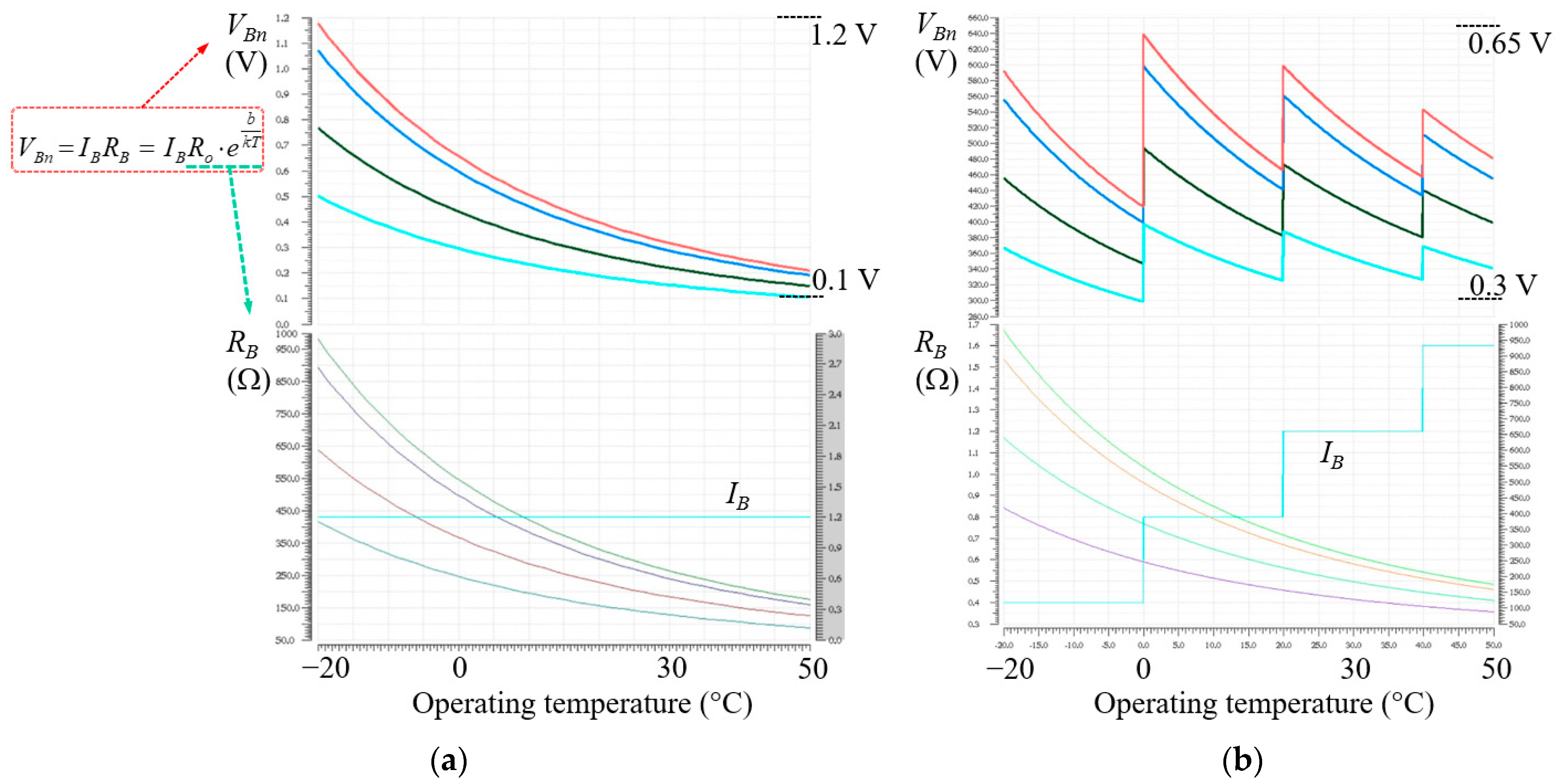
The resistance
RB of the target VO
x bolometer is modeled using Equation (1). Four bolometers are set up with a variation in
Ro and
b in Equation (1) of 10% each, and their characteristics are shown in the lower part of
Figure 7a. If
IB is independent of the operating temperature, the change in
VBn according to the operating temperature is equal to the change in
RB, as shown in the upper part of
Figure 7a. In this case, it is difficult to design a bias circuit and integrator because the range of
VBn is very wide. As shown in
Figure 7b, the range of
VBn can be significantly reduced by dividing the range of operating temperatures into four sections and using different
IB values for each.
IB values for each section do not need to be constant because the deviation of
IB is corrected, as demonstrated in
Section 3.
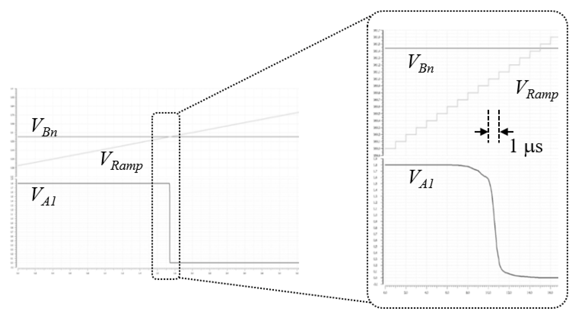
Figure 8 shows the process of determining
VBn during start-up calibration. After
VBn is determined by
IB, a rising ramp signal,
VRamp, is supplied from the bias circuit. When the
VRamp value becomes equal to
VBn, the output voltage
VA1 of comparator
A1 changes, and the digital value of
VBn is stored in the 12-bit memory of each unit circuit. Considering the speed of comparator
A1, the step time of
VRamp is set to 1 μs, and the time taken to determine the
VBn of the entire array is less than 70 ms. Therefore, the frame rate for determining
VBn is approximately 14.3 Hz, and real-time NUC is possible, as mentioned in
Section 3.4. The DC offset effect of comparator
A1 observed in
Figure 8 compensates for itself when fed to the corresponding bolometer after
VBn transmission.
Figure 9 shows the simulated waveforms for verifying the unit cell circuit in the operation mode, which were previously described in
Figure 4 and
Figure 6. The period for
VBn transmission is set using signal
ϕB, and the
IS integration time is determined using signals
ϕRST and
ϕH. When
ϕH changes to logic ‘0′, the integration voltage
V(
CINT) remains constant. After the integration of
IS, a 12-bit SS A/D conversion is performed using a row-level circuit for the ADC and comparator
A2. The output voltage
VA2 of
A2 controls the enabled terminal of the 12-bit memory.
Figure 10 shows the mask layout of the proposed unit cell circuit shown in
Figure 4. As the pixel size is (17 μm)
2, the size of the unit cell circuit is {68 (= 17 × 4) μm}
2. The integrator and comparator in
Figure 10 are marked based on the operation mode, and the capacitors occupy most of the layout.
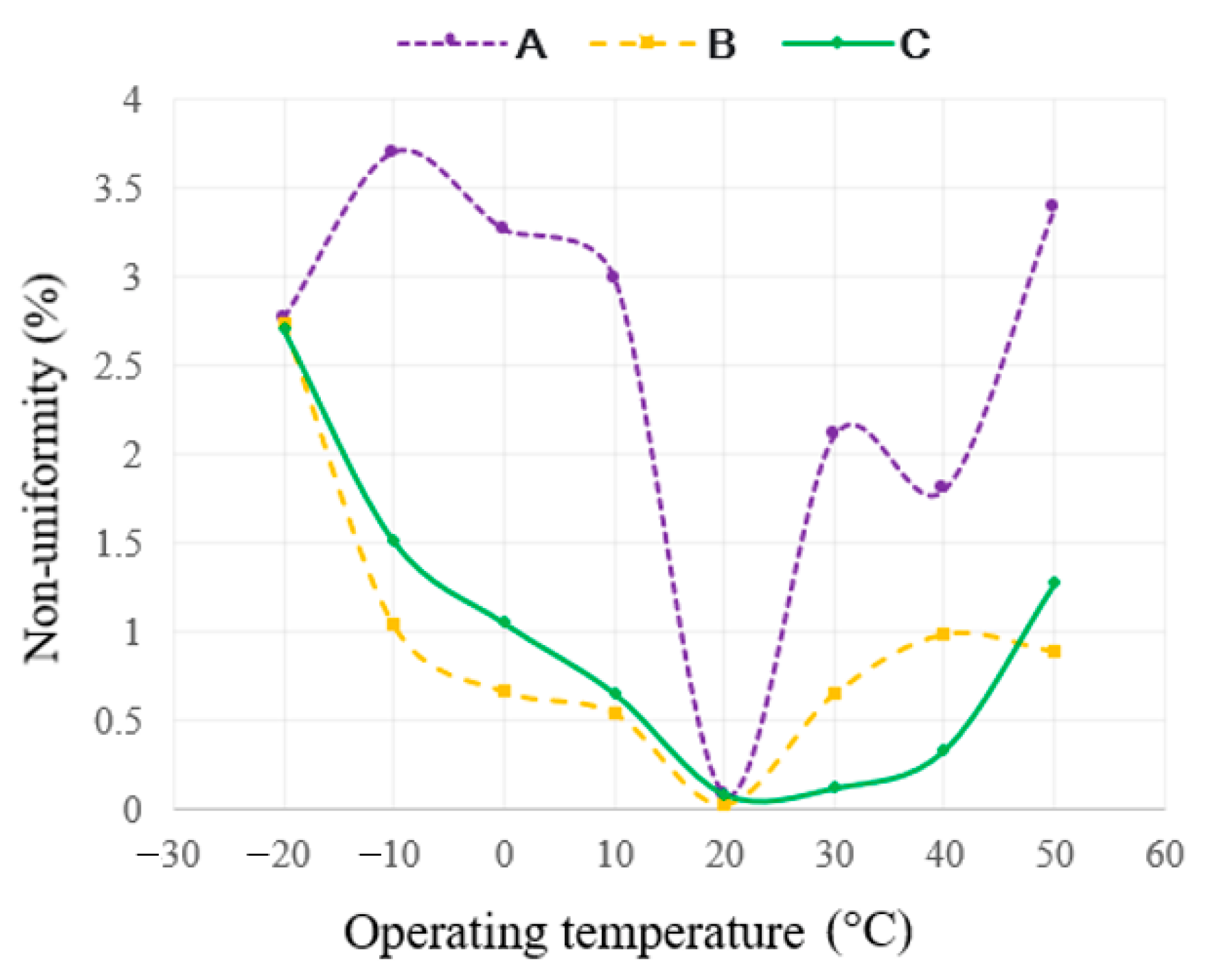
To verify the proposed NUC method, corner simulations are performed using the Cadence Virtuoso. For a conventional calibration method that uses a single correction coefficient table to perform a two-point correction, if the operating temperature changes in the absence of a TEC, the correction table will not fit, and the non-uniformity will increase.
Figure 11 shows the non-uniformity of the final digital signal obtained by applying the conventional calibration method to a bolometer with non-uniformity, as shown in
Figure 7. The correction coefficient is set according to the operating temperature of 20 °C, and
Figure 11 shows that the greater the difference between the operating temperature and 20 °C, the greater the non-uniformity. The offset correction in
Figure 11 uses the
VBn adjustment method, as in the proposed method. In this case, the charge feed-through and leakage current caused by the
ϕB switch generated during the
VBn transmission-and-hold process may affect the correction accuracy. Therefore, three types of
ϕB switches are designed, which are denoted as A, B, and C in
Figure 11, indicating an NMOS switch, CMOS switch, and NMOS switch with a dummy switch, respectively.
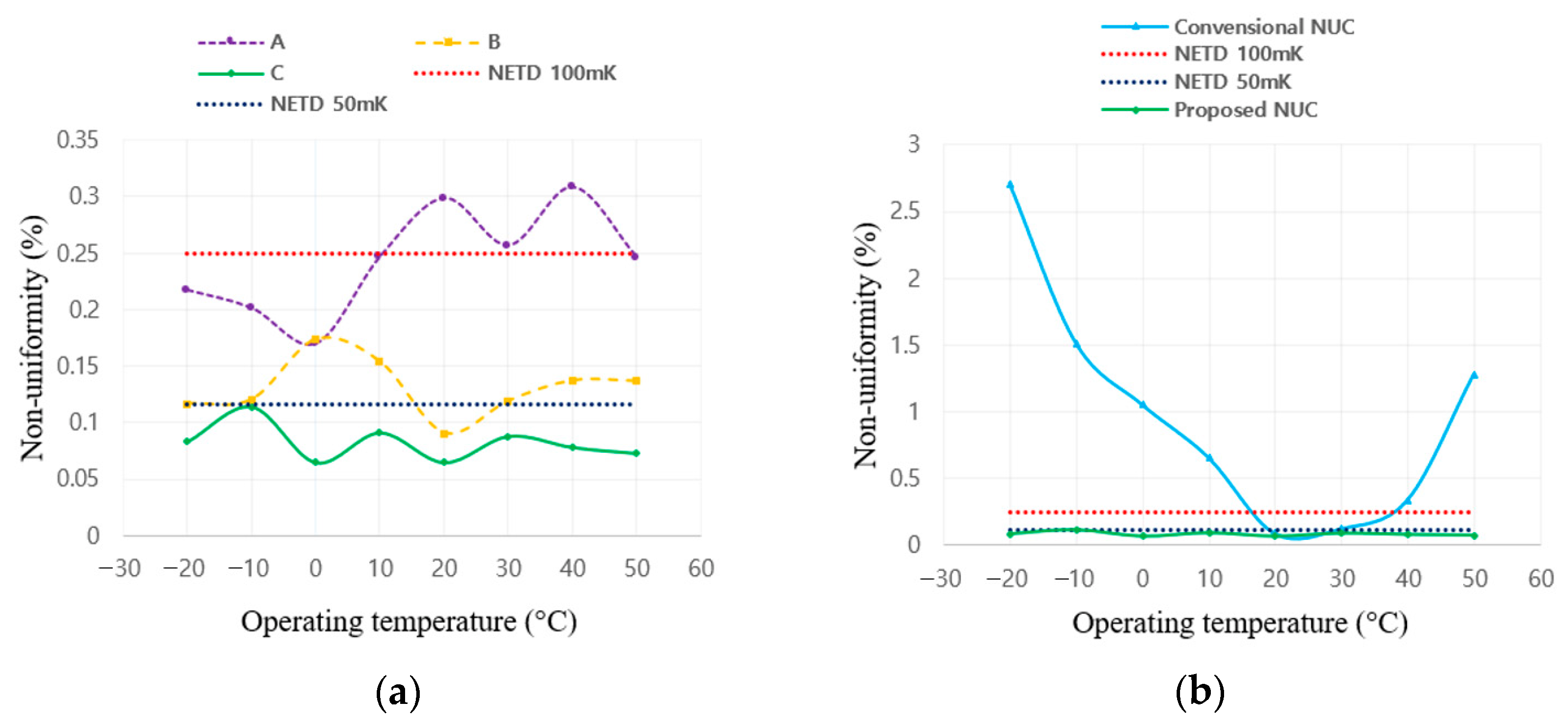
Figure 12a shows that non-uniformity is greatly decreased by the proposed NUC. A table for
βn is obtained by the calibration in production, as shown in
Figure 3a, at an operating temperature of 25 °C, and
αn is obtained by the start-up calibration shown in
Figure 3b, at an operating temperature of 20 °C.
Table 2 shows the
βn and
αn for the four bolometers shown in
Figure 7. Subsequently, the non-uniformity according to the operating temperature is observed by applying the same
αn, regardless of the operating temperature. When using the C switch, the transmission and hold of
VBn are most accurate, and non-uniformity also decreases relatively. The noise equivalent temperature difference (NETD), which can be used as a measure of non-uniformity, is the smallest possible temperature difference that a thermal imager can resolve. The smaller the NETD value, the higher the image resolution. The most frequently used limiting criteria for NETD are 50 and 100 mK, and the corresponding non-uniformities for these two values are shown in
Figure 12a.
Figure 12b compares the non-uniformity between the conventional NUC and the proposed NUC and shows the superiority of the proposed NUC.
Table 3 shows the performance comparison between the proposed NUC and other methods.


