Abstract
Current source topologies have several advantages compared to conventional voltage systems. Their inherent voltage-boosting function, intrinsic short-circuit protection, no electrolytic capacitor, direct-current control, continuous input current, and high reliability make them exceptional candidates for power generation systems, particularly for photovoltaic applications. This study provides an overview of the current source topologies for multi-stage photovoltaic grid-connected systems by comparing the number of components, performance, power-decoupling techniques, efficiency, and frequency operation. The overview reveals gain, performance, energy quality and lifetime improvements, thereby providing current source systems as an attractive alternative for renewable applications.
1. Introduction
Today, renewable energy is a favorable solution for providing green energy to address global power issues [1]. Photovoltaic (PV) power generation systems are trending technologies owing to their efficiency, projection, suitability, practicality, and use [2]. The PV systems are divided into two principal groups [3]: standalone systems, which operate independently, and interconnected systems, which operate in parallel with the electric utility grid [4].
The interconnected systems are classified based on the number of stages in power processing, use of transformer, transformerless configurations (to provide galvanic isolation between panel terminals and AC line), and type of commutation used. Thus, topologies that depend on the number of stages in energy processing are divided into single- and multistage systems, as shown in Figure 1.
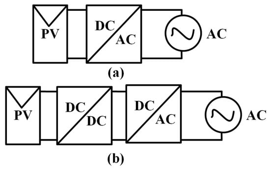
Figure 1.
Types of PV inverters: (a) single stage, (b) multi stage [5].
The boosting voltage level, processing of the maximum power point tracking (MPPT), and injected voltage waveform are included in the system capabilities shown in Figure 1. It should be noted that the key to using a single stage is to avoid a bulky transformer to reduce the size, weight, and power losses [6]. However, these inverters have drawbacks, such as low DC voltage range, poor power quality, and reduced power-processing capability.
In contrast, multi-stage inverters (Figure 1b) have galvanic isolation between the PV source and the grid to avoid common ground problems, protect power semiconductor devices, and boost the input voltage [7]. In addition, to interconnect DC and AC components, the system must inject an AC component with proper voltage magnitude, frequency, and phase into the grid network. This can generate more power losses owing to the saturation of magnetic cores [8] and thus needs compliance with international standards to ensure the correct interconnection. Table 1 lists some of these standards [9].

Table 1.
Standards of PV-interconnected systems.
Voltage and current-fed converters are part of the applied power topologies from Figure 1b [10,11,12,13,14]; among the two, the voltage ones are widely used systems because of their simple design and control. However, current source topologies provide numerous attractive features [15], such as inherent short-circuit capability, no electrolytic capacitor, step-up voltage capability, and continuous input current, which renders them as an interesting alternative not only for PV systems, but also for all DC-AC long lifetime applications.
In this context, this study provides an overview of the current source topologies for PV grid-connected systems by comparing the number of components, efficiency, complexity, reliability, and frequency operation with their conventional counterparts. The overview reveals the reliability, short-circuit protection, input current, voltage boosting, THD, and grid-integration improvements, thus providing current source systems as an attractive alternative for renewable applications.
The remainder of this study is organized as follows. Section 2 presents a comparison of the DC-DC stage between the non-resonant, quasi-resonant, and resonant converters. Section 3 presents some differences between the two principal DC-AC inverters: voltage and current inverters; additionally, it presents part of the principal characteristics of the latter. Finally, Section 4 presents the summary and concluding remarks.
2. DC-DC Power Converters
2.1. Non-Resonant DC-DC Power Converters
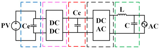
Figure 2.
Conventional scheme used for multi-stage PV-connected applications.
Based on the conventional scheme shown in Figure 2, the first stage () allows a low-frequency ripple. The second stage increases the voltage level of the PV according to the inverter specifications. The third and fourth stages represent the decoupling capacitor () and inverter, which must fulfill the following functions: (1) to shape the current into a sinusoidal waveform, and (2) if the PV array voltage is lower than the grid voltage, the PV array voltage must be boosted with an additional element. Finally, the fifth stage filters the sinusoidal signal.
In single-phase PV-connected applications, has critical importance because it must store the necessary energy to buffer the inherent time-varying double-line frequency ripple from the AC port [16]. Therefore, the decoupling component commonly used is an electrolytic capacitor, which reduces the lifetime of the system but is necessary to conserve energy. This point is critical because the application is generally used for power decoupling, a bulky and low reliable electrolytic capacitor, which considerably reduces the lifetime of the application [17].
For PV applications in the DC-DC stage, the pulse width modulated (PWM) converters are among the most applied topologies. One example is the boost converter [18,19]. This topology has advantages, such as low cost, low number of elements, and relative simplicity of design and implementation, which renders them suitable for the PV applications. However, issues, such as hard switching, severe reverse recovery in the output diode, limited efficiency, low power density, and low voltage gain, render it a viable option for low-power applications.
Other topologies used are the conventional and active flyback converters [20,21], whose particular characteristics in low-power applications are the well-coupled transformer, simplicity and low cost. However, issues, such as the high-voltage stress, reverse recovery loss, discontinuous input current (such as buck and buck-boost), large air gap for high power applications, and leakage inductance energy loss, do not render them a strong candidate for PV applications.
Similar to a flyback, the forward converter exhibits a high step-up voltage for low power applications [22]. Nevertheless, the energy is not transferred in a whole switching period, which not only increases the peak current, but also decreases the efficiency of the converter. Alternatively, Ćuk and SEPIC converters have a continuous input current [23,24], a characteristic that is fundamental for maximum renewable source energy extraction [25]. However, the Ćuk converter has an inverted output voltage, whereas SEPIC presents several constraints that need to be considered during its design.
From the above characteristics, Table 2 lists a comparison between DC-DC PWM voltage source and current source converters (VSC and CSC respectively).
Table 2.
Characteristics of DC-DC PWM converters.
Table 2 summarizes that PWM topologies for PV applications are required to be designed at low switching frequencies to avoid high power losses. In this context, the trend of increasing the switching frequency to demand an optimal weight, size, cost, and power density is not completely in agreement with PWM converters. However, topologies with continuous input current, such as SEPIC, Ćuk, and Zeta converters, are preferred for maximum renewable source energy extraction. On the other hand, for low power levels in which galvanic isolation is required, flyback, forward and push-pull converters are still popular.
A different category of DC-DC converters exists, where the switching frequency can be chosen to be as high as several hundred kilohertz, particularly for certain applications where high power density is of primary concern. These DC-DC converters are quasi-resonant.
2.2. Quasi-Resonant DC-DC Power Converters
In contrast with PWM topologies, for a quasi-resonant converter, the zero voltage switching and zero current switching techniques (ZCS and ZVS) are performed by applying an resonant array across the switch [40], where the injected energy is exchanged between the inductor and capacitor in a periodic sinusoidal form. Therefore, the current or voltage waveform of the semiconductor is forced to oscillate almost into a sinusoidal waveform, thus creating switching conditions at zero current or voltage during turn-on and turn-off instances; hence, semiconductor turn-off power losses are reduced.
Another characteristic of quasi-resonant converters is high-frequency operation without an increase in power loss. This characteristic reduces the reactive components of the topology and increases the power density of the system with less switching-voltage stress and noise [41].
The tank can be used as a lossless waveform device, where the resonance condition always appears at the turn-on instance. For this arrangement, if an ideal switch is implemented in the M- or L-type configuration (Figure 3a), and an anti-parallel diode is added, the voltage across is clamped by to positive, with the resonant switch operating in a half-wave mode (Figure 3b). However, if is implemented in series with , the resonant switch operates in the full-wave mode (Figure 3c).
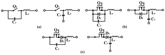
Figure 3.
Voltage mode resonant switches: (a) m-type, l-type configurations, (b) half-wave mode, and (c) full-wave mode.
As shown in Figure 3, when the resonant switch is turned on, the voltage can saturate before the current gradually increases in approximately a sinusoidal manner. Because of the resonance between and , the current through tends to oscillate to a negative value, aiming for to have a natural commutation, and the turn-off state is determined by the resonant frequency (), which cannot be freely varied. A common topology obtained by applying a resonant switch is the boost converter [42,43,44] (Figure 4a). This topology can be analyzed as a constant current () that feeds a voltage load (Figure 4b). By adding and through , the quasi-resonant topology performs ZVS (Figure 4c).
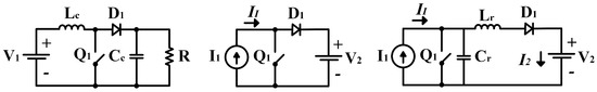
Figure 4.
Boost converter: (left) common structure, (middle) steady-state equivalent circuit, and (right) ZVS quasi-resonant converter.
The converter shown in Figure 4c has four operating modes. For the first mode (Figure 5a), and are off and flows into , thus linearly increasing its voltage (). The second mode (Figure 5b) describes the resonance state when is conducted by driving a portion of to . In this mode, the voltage across the inductor () and the current across () are the differences between - and -, respectively. In the third mode (Figure 5c), is discharged and its time is determined when reaches zero. Finally, in the fourth mode (Figure 5d), flows through and remains constant until turns off.
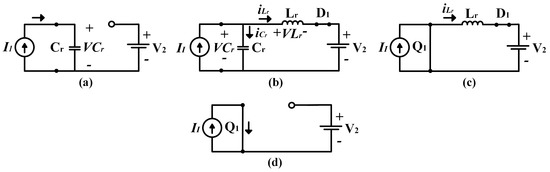
Figure 5.
Operation modes: (a) charging of , (b) resonant mode, (c) discharging of , and (d) freewheeling mode.
The quasi-resonant buck converter [45,46] (Figure 6a) is another topology whose switching period consists of four operating modes. In the first mode (Figure 6b), is turned on, which allows the inductor to be charged with input current . The second mode is the resonance condition performed by the series , array (Figure 6c). During this time, the input current increases its value, diode is off, and the difference between and flows across (), which causes a sinusoidal increment of . In the third mode (Figure 6d), is turned off, which generates to be discharged and causes the energy stored in to flow directly to the load until decreases linearly to zero. Finally, in the fourth mode (Figure 6e), the output current flows, which causes to conduct concluding the switching cycle of the converter.
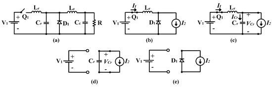
Figure 6.
Topology and operation modes: (a) quasi-resonant buck converter, (b) charging of , (c) resonant mode, (d) discharging of , and (e) freewheeling mode.
Similar to the quasi-resonant boost and buck converter, the common quasi-resonant buck–boost topology (Figure 7a) tends to reduce power losses, thereby providing a robust system with an excellent transient response and noise immunity by applying a ZCS condition [47,48]. Therefore, the new quasi-resonant buck-boost topologies develop an arrangement with a reduced capacitor size, whose inverter is generally composed of two interleaved converters with a smaller number of components for its implementation.
Figure 7.
Quasi-resonant topologies: (a) buck–boost, (b) forward, (c) flyback, (d) Ćuk, and (e) SEPIC.
Other quasi-resonant topologies are based on the forward (Figure 7b), flyback (Figure 7c), Ćuk (Figure 7d), and SEPIC (Figure 7e) converters [49,50,51,52,53,54]. These topologies eliminate most of the issues encountered in PWM systems because of their fast response for the dynamic PV system, soft-switching operation, reduction in voltage stress, high voltage gain, and high power density. However, some quasi-resonant topologies still have poor cross-regulation, are limited to discontinuous conduction mode (DCM), have a challenging electromagnetic interference (EMI) filter design, require a high output capacitance, and present high input current ripple. The major causes of losses are switch turn-off and diode reverse recovery, which is a significant disadvantage for many of these converters.
Table 3 lists a general summary of some quasi-resonant topologies reported in the literature.
Table 3.
Characteristics of DC-DC quasi-resonant power converters.
Quasi-resonant DC-DC converters offer to PV-connected applications, operating at high switching frequency, high voltage gain, low input ripple, low transformer turn ratio, and low current stress on switches to reduce the size of the magnetic components and increase power density. Full-bridge, half-bridge, and push–pull converters are the most utilized topologies [62], which achieve soft commutations and reduce the negative impacts of high ripple current, providing high efficiency over a considerable range of power ratings.
2.3. Resonant DC-DC Power Converters
Resonant power converters are suitable for medium- to high-power applications and have numerous benefits compared to the conventional PWM converters, such as low EMI, low switching losses, low volume and weight, high operating frequency, and low reverse-recovery losses [63]. These resonant converters can be divided into two categories: voltage-fed DC-DC resonant converters (VFRC), which have fewer components, higher efficiency, and higher frequency operation; and current-fed DC-DC resonant converters (CFRC), which do not present a pulsating input current but require a large inductor to feed the inverter.
One VFRC that applies a series LLC resonant tank, which achieves ZVS operation of the primary switches and ZCS operation of the rectifier diodes, is presented in [64]. However, the hold-up time presents an unfavorable effect on the efficiency because the DC/DC conversion stage should cover a wide range of input voltages. Similarly, full- and half-bridge resonant converters can run over an extensive input voltage capacity and a considerable load range while keeping excellent efficiency [65,66,67].
Another VFRC is the LLCC series-parallel resonant converter [68,69], which uses a full-bridge inverter connected to a half-bridge rectifier and transformer. This converter operates at a high frequency, which allows for a considerable decrease in the size of its magnetic elements. Furthermore, it presents the ZVS and ZCS in MOSFETs and diodes.
In contrast to the VFRC, the CFRC uses parallel resonant tanks and unidirectional switches that apply IGBTs, BJTs, or an array of MOSFET in series with a diode. These converters present ZVS, and in comparison, with other resonant converters, use only two choke inductors instead of the push–pull current source inverter, and only two grounded switches instead of the full bridge. One of these topologies that can be applied in an interconnected PV system is the current source parallel resonant converter (CSPRC) [70], wherein the AC load can be connected in parallel with a resonant capacitor. If the quality factor (Q) of the resonant tank is higher and the switching frequency is close to the resonant frequency, the output voltage applied to the load is almost sinusoidal. The topology is shown in Figure 8.
Figure 8.
Resonant converter. (a) CSPRC, (b) adding transformer and rectifier.
The circuit in Figure 8 is comprised of four stages: The first stage consists of a DC input current source () forming by the DC input source () and the choke inductor (). The second stage consists of a parallel resonant tank (, , ) which converts the square-wave voltage ( and ) into a sinusoidal output voltage () and , represents the DC power; also, the magnetic isolation is derived by , where A and B are coupled to C and D. The third stage consists of a full-wave rectifier (, , and , ), where the input power is in phase with the input voltage and contains only the fundamental component of the square-wave input current. Finally, the fourth stage consists of the decoupling elements ( and ).
The CSPRC, compared to conventional non-resonant topologies, provides a continuous input current with a very low AC ripple, does not present stability problems, and due to the use of the parallel resonant tank, presents a natural array with transformers, which is desirable for PV-connected applications. However, the resonant tank and the components used need to be carefully selected since these parameters affect directly the overlapped signals in the two bidirectional two-quadrant switches ( and ). Therefore, slightly overlapping gate-to-source voltages should be used.
Similar to the CSPRC, the current-fed push–pull converter is another topology that is suitable for PV-connected applications, owing to its small ripple of both an input current and output voltage with fewer components. In comparison with the voltage-fed push–pull converter, only an input inductor to obtain a small ripple of the input current and an output capacitor to obtain a small ripple of the output voltage is necessary [71]. As the primary side voltage is higher than the input source voltage, the copper loss and leakage of the transformer are reduced.
In contrast, the performance of the traditional current-fed push–pull converter is affected by issues, such as voltage spikes of switches, high-voltage stress, reverse recovery, and low power conversion. As the duty cycle needs to be 50%, the operating range of the input voltage is relatively narrow. However, applying a voltage-doubler rectifier in combination with resonant techniques enables achieving soft-switching techniques and removes the reverse-recovery problem, thereby providing a topology with a higher voltage conversion ratio and efficiency.
A focused work in a current-fed push–pull converter was presented in [72], which presented a topology (Figure 9) to decrease the switching losses and turn ratio of the transformer by applying soft switching of the primary switches (, ) and a voltage doubler of the secondary side.
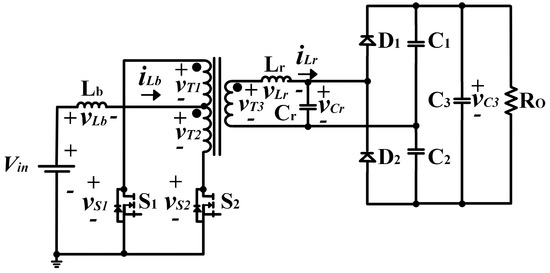
Figure 9.
Push–pull converter.
The topology in Figure 9 comprises switches and , a current source (), a voltage-doubler diode (, ), an resonant tank (, ), and a transformer, whose primary side voltages (, ) are the sum of the input voltage () and . This topology reduces the switching losses by applying ZVS and ZCS and presents continuous input current, high voltage gain, fewer components, natural isolation arrangement, and high efficiency, which results in a proper topology for PV-connected applications.
Similar to the current-fed push–pull converter, the high step-up current-fed converter decreases switching losses by applying ZVS and ZCS [73]. In addition, the arrangement in the transformer reduces the weight and volume, has a higher voltage gain with a lower transformer turn ratio, and reduces the complexity in the control stage by applying only two switches [74].
An example of a high step-up current-fed converter is presented in [75], which presents a new ZVS current-fed isolated push–pull converter, where all switches are in the on-state under ZVS and ZCS, and the off-state under almost ZVS. Moreover, the topology absorbs the voltage across its main switch, thus exhibiting high efficiency and high gain voltage. The circuit is illustrated in Figure 10.
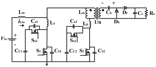
Figure 10.
High step-up current-fed converter.
In Figure 10, , are the main switches and CS1, CS2 represent their snubber capacitors; , are the leakage and magnetizing inductances, respectively; , are the auxiliary switches; , are the clamp capacitors; is the blocking capacitor; , is the secondary-side transformer diode; and is the output capacitor.
A main feature of the circuit shown in Figure 10 is its ability to absorb the leakage inductance energy and clamp the voltage stress across the switches, thereby reducing the switching losses and improving the power density. In addition, it presents a high-voltage gain, high efficiency, and low input current ripple, which renders the topology suitable for high-power applications with low input and high output voltages, such as PV systems.
Based on the above description, Table 4 lists some characteristics offered by the DC-DC resonant converters, Table 5 lists comparison indices for VSC and CSC used in PV-connected applications, and Table 6 lists some features and drawbacks offered for current-fed topologies.
Table 4.
Characteristics of DC-DC resonant power converters.
Table 5.
Comparison indices between DC-DC CSC and VSC.
Table 6.
Features and drawbacks of current-fed topologies [83,84,85,86].
3. MPPT for DC-DC Power Converters
As MPPT is an essential capability for PV power generation systems, classifying the different algorithms reported in the literature is essential to determine their performance. Thus, ref. [91] classified MPPT methods for PV systems into three categories: offline, online, and hybrid. The offline method uses the physical values of the PV system to generate control signals, the online method requires instantaneous values of the output voltage, and the hybrid method requires a separate algorithmic loop.
From this classification, the classical algorithms used in some PWM converters are perturb and observe (PO) [92], fractional open-circuit voltage [93], fractional short-circuit current [94], and incremental conductance [95]. However, in contrast to conventional PWM converters that are modulated by the variation in duty cycle, the quasi-resonant and resonant converters must be controlled with frequency modulation [96].
Frequency-based MPPT algorithms increase the system complexity owing to the voltage maximum power point (MPP) variation, which requires a DC-DC converter that allows variations in its effective input resistance. Hence, as the resonant converters have to work very close to the resonance condition, the switching and resonant frequencies must to be close. This can affect the interval of variation in switching frequency and the values of the resonant components, which can drastically reduce the number of topologies that can be applied.
In addition, the literature reports some applications of tracking the MPP for PV systems by applying fuzzy logic controllers [97], neural networks [98], evolutionary algorithms [99], and hybrid methods [100]. Thus, it exhibits a faster converging speed, good performance and efficiency, fewer oscillations, and no convergence from the MPP under varying weather conditions. For these conditions, particularly for partial shading conditions (PSC), the literature summarizes some strategies based on PSC into four categories.
- Hardware and control methods based on array reconfiguration.
- Control method based on artificial intelligence algorithms.
- Improved direct control methods based on perturbation self-optimization.
- Some MPPT methods based on partial shading detection schemes.
From the previous overview, Table 7 lists the MPPT algorithms classified based on the topology to be implemented.
Table 7.
MPPT algorithms for PV-connected applications.
4. DC-AC Inverter
For PV-connected applications, the DC-AC inverters can be classified into self- and line-commutated inverters [117]. The self-commutated inverter transfers the current and controls the turn-on and turn-off conditions by applying both an H-bridge arrangement and a PWM technique. In contrast, the grid network dictates the commutation process for the line-commutated inverter, thus controlling the turn-on and turn-off conditions using an additional circuit.
Self-commuted inverters are classified into the following two types: first, voltage source inverters (VSIs), which can be designed by an input parallel-capacitor with a discontinuous input current () (Figure 11a); and second, current source inverters (CSIs), which can be designed by a bulky series inductor, where its input side is fed with a constant DC source with the same polarity, thus aiming that the is continuous (Figure 11b).
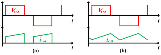
Figure 11.
Voltage and current representation over one switching period at the entrance of the inverter: (a) VSI and (b) CSI.
From Figure 11 the CSI can apply the or filter, as compared to the VSI, which has the diagonals switched with a certain dead time and generally uses an filter. However, for a single-phase multistage PV-connected system, the pulsating energy manifests itself as a current or voltage ripple for a CSI or VSI, respectively, which generates problems related to the filtering stage, size of passive elements, power losses, quality of the power signal, and performance.
In this regard, for an interconnected single-phase system, a low power ripple will cause a DC-link current or voltage ripple for the inverter because the grid voltage and current are defined as
where V and I are the voltage and current supplied by the inverter; is the angular frequency (AC); and is the offset angle between V and I. Thus, the instantaneous power flow is
Equation (3) shows the instantaneous power flow considering the time intervals at which the power varies at twice the line frequency. This oscillating ripple degrades the performance of MPPT, and affects the extraction efficiency in single phase PV inverters [118], thereby causing the decoupling DC component to have a high energy density. Thus, in several cases, the use of an electrolytic capacitor is required [119]. Nevertheless, as described above, these capacitors have several disadvantages, which reduce the lifetime of the system [120], thus rendering them undesirable for application.
4.1. The Typical Voltage Source Inverter
The conventional VSI [121] is composed of a power-decoupling component (), a current source (), four bidirectional voltage switches (–), an output filter (), three parasitic resistances , , and , and a switch to interconnect the inverter with the utility grid (Figure 12). The averaged mathematical model of the VSI was defined by applying Kirchhoff’s voltage and current laws, as shown in Equation (4).
where u is the duty cycle with values between . Considering that the VSI is decoupled with the DC/DC converter, the direct current bus () is constant.
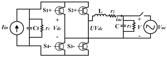
Figure 12.
Typical VSI.
The VSI can operate in the voltage control mode (VCM), also known as grid-forming, and the current control mode (CCM), known as grid-following, where both modes can be applied to an interconnected system [122]. However, CCM is used commonly because it exhibits s better suppression of the current ripple and energy control, thus providing a higher power factor. In addition, the polarity of the input current on the DC side determines the direction of the average power flowing through the inverter; however, the VSI is not entirely compatible with low-power single-phase applications because the input voltage is typically lower than the peak voltage of the grid network.
4.2. Typical Current Source Inverter
The common CSI [123] (Figure 13) is composed of a DC voltage source (), an inductor () that absorbs the voltage harmonics produced by the CSI, four unidirectional switches (, , and , ), and an output filter (C and L) with parasitic resistances , , and . The mathematical model is given by Equation (5). In this case, the complexity of the model concerning the VSI is evident because there is a non-linear model, that is, there are products of state variables with the control signal. This type of model is known as a bilinear system [124,125].
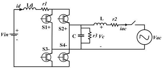
Figure 13.
Typical CSI.
In Figure 13, power decoupling is realized by applying a DC-link inductor, which retains the input current through the inverter instead of the electrolytic capacitor in a VSI. In addition, the CSI draws a continuous input current, which makes it suitable for renewable applications. This current generates an AC waveform, where is charged during the shoot-through periods and discharged during normal conduction.
Additionally, the CSI can operate without the need of a previous DC-DC converter while the input voltage is under the peak value of the grid voltage. However, the input current ripple of the inductor increases as a result of the switching frequency and inductance values, and the control is more complex compared to the VSI because the control variable appears in both the inductor-current and capacitor-voltage equations.
Based on previous characteristics, the literature shows important contrasts between VSI and CSI. Some of these characteristics are listed in Table 8.
Table 8.
Differences between VSI and CSI [117,118,119,120,121,122,123,124,125,126].
According to Table 8, the CSI presents important characteristics that make it a good alternative for renewable applications than the commonly used VSI. Therefore, there is a need to study the feasibility of these systems with the aim of determining the main characteristics and drawbacks that they offer to PV-connected applications. Some of these studies are described below.
4.3. Inverter Topologies Fed by a Current Source
According to the literature, the use of CSI can potentially eliminate the decoupling electrolytic capacitor used by the VSI, thereby resulting in numerous benefits [127]. One study focused on this issue is presented in [128], which offers a power-decoupling circuit viewed as a controlled voltage source in series with a DC inductor. The topology is shown in Figure 14.
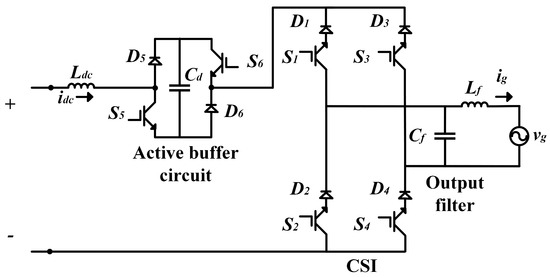
Figure 14.
Single-phase current source converter.
The topology in Figure 14 comprises an active buffer circuit that consists of four power semiconductor devices (, , and , ) and an active buffer capacitor () that absorbs the power pulsation with a twice-line frequency. The switching modes of the circuits are presented in Table 9.
Table 9.
Switching modes in the current source converter.
As per Table 9, in Modes 1 and 3, is disconnected from the main circuit and buffer, and works as a freewheeling path. In Mode 2, is charged by absorbing the excess energy provided by the utility grid. Finally, in Mode 4, is discharged, and the insufficient energy required by the load is supplemented.
This type of topology presents a possibility to replace the original electrolytic capacitor with a film capacitor with a low rated voltage, which can extend the lifetime and reduce the size and weight of the system.
Another advantage of CSI is the possibility to reduce the input current ripple [129]. The study involving it explains the performance of a CSI with six voltage bidirectional switches comprised of three upper (, , and ) and three lower switches (, , and ), as shown in Figure 15.
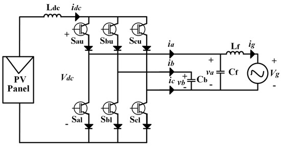
Figure 15.
CSI with six voltage bidirectional switches.
The circuit in Figure 15 implements a current source () whose size depends on the switching frequency. The voltage of section b () is connected to the grid by and the inverter is interconnected through an filter, which comprises and . The work in Figure 15 is presented to have a low-frequency ripple by comparing the link () and a reference current, as well as a component of the grid current calculated from the reactive power, which ensures that among the currents , , and , can achieve a continuous power flow. However, one critical issue in this type of topology is the performance and power oscillation on the DC link, which results in a bulky inductor, whose main drawbacks are low power density and dynamic response degradation. Thus, an effort focused on proposing solutions to the aforementioned problems is reported in [130], whose main contribution is an active power filter (APF) to compensate for power ripple.
This work is shown in Figure 16, and presents an auxiliary circuit (APF) as a novel power decoupling by applying the typical H-bridge CSI, and an active voltage regulator (AVR) connected to the grid voltage (vg) through the filter ( and ).
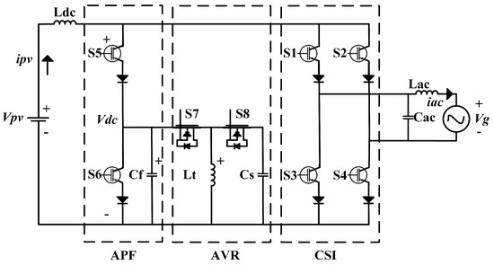
Figure 16.
Power decoupling circuit for CSI.
As shown in Figure 16, the APF circuit has one phase leg connected to the CSI and an auxiliary DC source (). In addition, a bidirectional buck–boost converter comprises the AVR (in discontinuous current mode), with an energy transfer inductor () and an energy storage capacitor (), performing an optimal power density, aiming for an important size reduction in the passive components.
However, according to the literature, the use of a CSI negatively impacts the inverter efficiency because presents high conduction losses due to its high levels of current during its control stage [131]. In this regard, a study focused on passivity-based control (PBC) was conducted [132]. This proposal maintained an output voltage with fast dynamic response, continuous-time domain, negligible sensitivity, guaranteed stability, good load regulation, no performance limitation, and low THD.
As mentioned earlier, the decoupling energy of a CSI compared to that of a VSI provides an attractive option for a longer lifetime, owing to the elimination of the electrolytic capacitor. Ref. [133] is a focused study on this issue, which introduces a different energy management by applying six bidirectional switches, excluding the filter at the output inverter. The electrolytic capacitor is replaced by managing the decoupling energy with the component , which is connected on the AC side to absorb the AC fluctuation, thereby allowing a smaller capacitor. The topology and switching modes are illustrated in Figure 17.
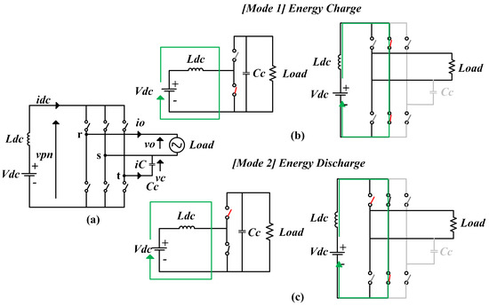
Figure 17.
Topologies: (a) structure of the single-phase current source inverter with power decoupling function, (b) boost technique of conventional circuit, (c) boost technique of the presented circuit.
The topology in Figure 17a comprises a direct input voltage () and current source (), six bidirectional switches and a film capacitor (); because works as a filter inductance, an output filter is not required. The principle of voltage boost can be explained by the commutations of the switches. Thus, as shown in Figure 17b, the DC voltage is increased by storing energy in (Mode 1) and discharging it through the upper arm (Mode 2). By contrast, in Figure 17c, the AC voltage is raised directly by (Mode 1) and discharged to the load (Mode 2), thus allowing a no longer step-up boost circuit. Finally, by controlling the capacitor current (), power flows to offset the component in the output power. Consequently, the input power becomes constant and does not fluctuate.
However, as mentioned earlier, the recognized issue of the leakage current in an interconnected PV system depends extremely on the value of the parasitic capacitance between the PV panel and the ground [134].
As shown in Figure 18, the potential differences produced by the switching states on the inverter inject leakage current on the DC and AC sides, which causes grid current distortion, losses in the PV system, electromagnetic interference (EMI), and harmonics injected into the utility grid. Consequently, consideration of the appearance of leakage current during the design of a PV-connected application becomes critical because the leakage current cannot be totally eliminated, but can be reduced.

Figure 18.
Simplified common-mode leakage current.
A precise focused study to reduce the leakage current is presented in [135], which presents a novel CSI with AC-side clamping (Figure 19).
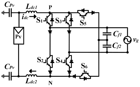
Figure 19.
CSI with AC-side clamping [135].
The circuit in Figure 19 comprises two DC-side inductors ( and ), six insulated-gate bipolar transistors (, , , and , , and ), and two AC-side filter capacitors ( and ). represents the AC-side voltage, and represents the parasitic capacitance between the PV system and the ground. This circuit reduces the leakage current and suppresses the switching-frequency common-mode voltage when the positive and negative DC-side buses (P and N, respectively) are clamped at the midpoint of the AC-side filter capacitors during the freewheeling period (when and are turned on, respectively).
As described below, there are some important issues to be considered when choosing the type of inverter to be implemented; these include power decoupling, number of switches, THD, and leakage current. In this regard, Table 10 shows some inverters presented for PV-connected applications, considering the work presented in [136].
Table 10.
Single-stage inverters for PV-connected applications.
According to Table 10, CSI is a good candidate for grid-interconnected systems because it does not require the use of electrolytic capacitors, which are essential for the lifetime of an application. In addition, with an active damping control or by applying an additional switch, it is possible to reduce the harmonic content, minimize losses, and attenuate the excitation of the LC filter. However, the limited acceptance of a bulky inductor and the need to use (sometimes) more power semiconductor devices are some of the issues that CSI must improve with the aim of consolidating itself for this application.
4.4. Control of Inverters
Control of the VSI and CSI can be classified into (a) grid forming and (b) grid following. Grid forming is responsible for fixing the voltage and frequency at the output, and grid following is responsible for injecting active and reactive power into the electrical network, as shown in Figure 20.
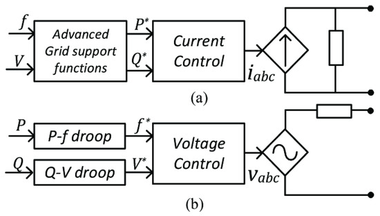
Figure 20.
Inverter controllers: (a) grid-following control with grid support functions; and (b) grid-forming droop control [122].
Grid-following inverters rely primarily on measuring the point of the connection voltage to be synchronized with the grid [140,141,142]. Apart from sensing the point of connection voltage, its phase angle and frequency are extracted using a phase-locked loop, which is subsequently used by a current controller [143,144,145,146].
However, grid-forming inverters exploit droop control for grid synchronization [147,148,149] and regulate the point of connection voltage as the frequency and magnitude of this voltage are provided by active and reactive power control loops, which operate primarily based on droop control [150,151].
Currently, most commercial PV inverters operate as grid-following sources that regulate their power output by measuring the angle of the grid voltage by applying a phase-locked loop [152]. Therefore, they simply follow the angle or frequency of the grid and do not actively control their frequency outputs. In contrast, a grid-forming source actively controls its frequency and is used extensively in microgrid setups.
5. Summary and Conclusions
Some main features offered for the current source topologies are listed below.
For current source DC-DC converters, they are as follows:
- Reliable auto short-circuit protection.
- A constant and continuous input current.
- A simple gate-drive circuit without requirement of isolation or optical couplers.
- A reduced leakage inductance.
- Inherent voltage boosting capability.
- A filter stage is not required to prevent the ripple current from being reflected in the PV system.
- Simple converter structure.
- Low switch count, low switching dv/dt.
- Controllable current at its output terminals.
- Smooth DC-output current.
For current source inverters, they are as follows:
- Better sinusoidal output voltage.
- Low THD.
- A reduced leakage current.
- High reliability and long lifetime owing to the use of a bulky inductor as a power-decoupling component instead of an electrolytic capacitor.
- A small filter is required on the AC side.
- Excellent grid-integration performance, such as sinusoidal current/voltage and fully controlled power factor.
- Inherent current-limiting capability.
- The DC-link inductor provides natural protection against short-circuit faults.
- Lower voltage stresses.
- Direct-current control capability, where AC current is controlled in magnitude and phase.Less switching loss.
- Avoids shoot-through damage.
- Lower operation and maintenance cost.
The advantages described above could be translated into a considerable increase in the reliability and lifetime of the system, thereby increasing the interest in these topologies that, according to the literature, represent the minority part of the systems studied for renewable energy applications. In this regard, the viability that the current-fed topologies present compared to that of the voltage-fed topologies, has to be considered and more research will be necessary to determine the real opportunities and limitations that these topologies can offer to the application.
Funding
The authors would like to thank the financial support from Programa de becas posdoctorales en la UNAM POSDOC, DGAPA-UNAM, Mexico, and by DGAPA-UNAM under grant PAPIIT IN109622.
Data Availability Statement
Not applicable.
Acknowledgments
This work was undertaken as part of the “Programa de becas posdoctorales” of Universidad Nacional Autónoma de México. The authors would like to thank the DGAPA-UNAM for supporting the research activities described in this paper.
Conflicts of Interest
The authors declare no conflict of interest.
References
- Cai, Y.; Huang, G.; Yeh, S.; Liu, L.; Li, G. A modeling approach for investigating climate change impacts on renewable energy utilization. Int. J. Energy Res. 2012, 36, 764–777. [Google Scholar] [CrossRef]
- Dincer, I. Renewable energy and sustainable development: A crucial review. Renew. Sustain. Energy Rev. 2000, 4, 157–175. [Google Scholar] [CrossRef]
- Xiao, W. Photovoltaic Power System: Modeling, Design, and Control; John Wiley & Sons: Hoboken, NJ, USA, 2017. [Google Scholar]
- Obi, M.; Bass, R. Trends and challenges of grid-connected photovoltaic systems—A review. Renew. Sustain. Energy Rev. 2016, 58, 1082–1094. [Google Scholar] [CrossRef]
- Kjaer, S.B.; Pedersen, J.K.; Blaabjerg, F. A review of single-phase grid-connected inverters for photovoltaic modules. IEEE Trans. Ind. Appl. 2005, 41, 1292–1306. [Google Scholar] [CrossRef]
- Meneses, D.; Blaabjerg, F.; Garcia, O.; Cobos, J.A. Review and comparison of step-up transformerless topologies for photovoltaic AC-module application. IEEE Trans. Power Electron. 2012, 28, 2649–2663. [Google Scholar] [CrossRef]
- Xiao, W.; El Moursi, M.S.; Khan, O.; Infield, D. Review of grid-tied converter topologies used in photovoltaic systems. IET Renew. Power Gener. 2016, 10, 1543–1551. [Google Scholar] [CrossRef]
- Barater, D.; Lorenzani, E.; Concari, C.; Franceschini, G.; Buticchi, G. Recent advances in single-phase transformerless photovoltaic inverters. IET Renew. Power Gener. 2016, 10, 260–273. [Google Scholar] [CrossRef]
- Basso, T.S.; DeBlasio, R. IEEE 1547 series of standards: Interconnection issues. IEEE Trans. Power Electron. 2004, 19, 1159–1162. [Google Scholar] [CrossRef]
- Forouzesh, M.; Baghramian, A. Galvanically isolated high gain Y-source DC–DC converters for dispersed power generation. IET Power Electron. 2016, 9, 1192–1203. [Google Scholar] [CrossRef]
- Geury, T.; Pinto, S.; Gyselinck, J. Current source inverter-based photovoltaic system with enhanced active filtering functionalities. IET Power Electron. 2015, 8, 2483–2491. [Google Scholar] [CrossRef]
- Sinha, A.; Chandra Jana, K. Comprehensive review on control strategies of parallel-interfaced voltage source inverters for distributed power generation system. IET Renew. Power Gener. 2020, 14, 2297–2314. [Google Scholar] [CrossRef]
- Ye, Y.; Cheng, K.; Chen, S. A high step-up PWM DC-DC converter with coupled-inductor and resonant switched-capacitor. IEEE Trans. Power Electron. 2016, 32, 7739–7749. [Google Scholar] [CrossRef]
- Zhang, N.; Sutanto, D.; Muttaqi, K.M.; Zhang, B.; Qiu, D. High-voltage-gain quadratic boost converter with voltage multiplier. IET Power Electron. 2015, 8, 2511–2519. [Google Scholar] [CrossRef]
- Dash, P.P.; Kazerani, M. Dynamic modeling and performance analysis of a grid-connected current-source inverter-based photovoltaic system. IEEE Trans. Sustain. Energy 2011, 2, 443–450. [Google Scholar] [CrossRef]
- Zhang, H.; Li, X.; Ge, B.; Balog, R.S. Capacitance, dc voltage utilizaton, and current stress: Comparison of double-line frequency ripple power decoupling for single-phase systems. IEEE Ind. Electron. Mag. 2017, 11, 37–49. [Google Scholar] [CrossRef]
- Georgitsioti, T.; Pearsall, N.; Forbes, I.; Pillai, G. A combined model for PV system lifetime energy prediction and annual energy assessment. Sol. Energy 2019, 183, 738–744. [Google Scholar] [CrossRef]
- Khazaei, P.; Modares, S.; Dabbaghjamanesh, M.; Almousa, M.; Moeini, A. A high efficiency DC/DC boost converter for photovoltaic applications. Int. J. Soft Comput. Eng. 2016, 6, 2231–2307. [Google Scholar]
- Padmanaban, S.; Blaabjerg, F.; Wheeler, P.; Ojo, J.O.; Ertas, A.H. High-voltage dc-dc converter topology for pv energy utilization—Investigation and implementation. Electr. Power Compon. Syst. 2017, 45, 221–232. [Google Scholar] [CrossRef]
- Shadmand, M.; Balog, R.S.; Rub, H.A. Maximum Power Point Tracking using Model Predictive Control of a flyback converter for photovoltaic applications. In Proceedings of the Power and Energy Conference at Illinois (PECI), Champaign, IL, USA, 28 February–1 March 2014; pp. 1–5. [Google Scholar]
- Zhang, J.; Huang, X.; Wu, X.; Qian, Z. A high efficiency flyback converter with new active clamp technique. IEEE Trans. Power Electron. 2010, 25, 1775–1785. [Google Scholar] [CrossRef]
- Tan, F.D. The forward converter: From the classic to the contemporary. In Proceedings of the APEC. Seventeenth Annual IEEE Applied Power Electronics Conference and Exposition (Cat. No. 02CH37335), Dallas, TX, USA, 10–14 March 2002; Volume 2, pp. 857–863. [Google Scholar]
- Banaei, M.R.; Sani, S.G. Analysis and implementation of a new SEPIC-based single-switch buck–boost DC–DC converter with continuous input current. IEEE Trans. Power Electron. 2018, 33, 10317–10325. [Google Scholar] [CrossRef]
- Sun, Z.; Yang, Z. Improved maximum power point tracking algorithm with cuk converter for PV systems. J. Eng. 2017, 2017, 1676–1681. [Google Scholar] [CrossRef]
- Williams, B.W. DC-to-DC converters with continuous input and output power. IEEE Trans. Power Electron. 2012, 28, 2307–2316. [Google Scholar] [CrossRef]
- Kasa, N.; Iida, T.; Chen, L. Flyback inverter controlled by sensorless current MPPT for photovoltaic power system. IEEE Trans. Ind. Electron. 2005, 52, 1145–1152. [Google Scholar] [CrossRef]
- Sukesh, N.; Pahlevaninezhad, M.; Jain, P.K. Analysis and implementation of a single-stage flyback PV microinverter with soft switching. IEEE Trans. Ind. Electron. 2013, 61, 1819–1833. [Google Scholar] [CrossRef]
- Shi, Y.; Li, R.; Xue, Y.; Li, H. Optimized operation of current-fed dual active bridge DC–DC converter for PV applications. IEEE Trans. Ind. Electron. 2015, 62, 6986–6995. [Google Scholar] [CrossRef]
- Prasanna, U.R.; Rathore, A.K. Analysis, design, and experimental results of a novel soft-switching snubberless current-fed half-bridge front-end converter-based PV inverter. IEEE Trans. Power Electron. 2012, 28, 3219–3230. [Google Scholar] [CrossRef]
- Zhang, Z.; He, X.F.; Liu, Y.F. An optimal control method for photovoltaic grid-tied-interleaved flyback microinverters to achieve high efficiency in wide load range. IEEE Trans. Power Electron. 2013, 28, 5074–5087. [Google Scholar] [CrossRef]
- Kim, Y.H.; Ji, Y.H.; Kim, J.G.; Jung, Y.C.; Won, C.Y. A new control strategy for improving weighted efficiency in photovoltaic AC module-type interleaved flyback inverters. IEEE Trans. Power Electron. 2012, 28, 2688–2699. [Google Scholar] [CrossRef]
- Tan, G.; Wang, J.; Ji, Y. Soft-switching flyback inverter with enhanced power decoupling for photovoltaic applications. IET Electr. Power Appl. 2007, 1, 264–274. [Google Scholar] [CrossRef]
- Elkhateb, A.; Abd Rahim, N.; Selvaraj, J.; Williams, B.W. DC-to-DC converter with low input current ripple for maximum photovoltaic power extraction. IEEE Trans. Ind. Electron. 2014, 62, 2246–2256. [Google Scholar] [CrossRef]
- Meneses, D.; Garcia, O.; Alou, P.; Oliver, J.A.; Cobos, J.A. Grid-connected forward microinverter with primary-parallel secondary-series transformer. IEEE Trans. Power Electron. 2014, 30, 4819–4830. [Google Scholar] [CrossRef]
- Radmanesh, H.; Soltanpour, M.R.; Azizkandi, M.E. Design and implementation of an ultra-high voltage DC-DC converter based on coupled inductor with continuous input current for clean energy applications. Int. J. Circuit Theory Appl. 2021, 49, 348–379. [Google Scholar] [CrossRef]
- Lahooti Eshkevari, A.; Mosallanejad, A.; Sepasian, M.S. Design, analysis, and implementation of a new high-gain P-type step-up dc/dc converter with continuous input current and common ground. IET Power Electron. 2021, 14, 225–238. [Google Scholar] [CrossRef]
- Radmanesh, H.; Soltanpour, M.R.; Azizkandi, M.E. A Continuous Input Current DC-DC Converter Based on Coupled Inductor for Renewable Energy Applications. In Proceedings of the 12th Power Electronics, Drive Systems, and Technologies Conference (PEDSTC), Tabriz, Iran, 2–4 February 2021; pp. 1–5. [Google Scholar]
- Yari, K.; Mojallali, H.; Shahalami, S.H. A new coupled-inductor-based buck–boost DC–DC converter for PV applications. IEEE Trans. Power Electron. 2021, 37, 687–699. [Google Scholar] [CrossRef]
- Mahmood, A.; Zaid, M.; Ahmad, J.; Khan, M.A.; Khan, S.; Sifat, Z.; Lin, C.H.; Sarwar, A.; Tariq, M.; Alamri, B. A non-inverting high gain DC-DC converter with continuous input current. IEEE Access 2021, 9, 54710–54721. [Google Scholar] [CrossRef]
- Kwon, J.M.; Choi, W.Y.; Kwon, B.H. Single-switch quasi-resonant converter. IEEE Trans. Ind. Electron. 2008, 56, 1158–1163. [Google Scholar] [CrossRef]
- Blinov, A.; Korkh, O.; Chub, A.; Vinnikov, D.; Peftitsis, D.; Norrga, S.; Galkin, I. High gain DC–AC high-frequency link inverter with improved quasi-resonant modulation. IEEE Trans. Ind. Electron. 2021, 69, 1465–1476. [Google Scholar] [CrossRef]
- Bellini, A.; Bifaretti, S. A quasi-resonant ZCS boost DC-DC converter for photovoltaic applications. In Proceedings of the IEEE International Symposium on Industrial Electronics, Vigo, Spain, 4–7 June 2007; pp. 815–820. [Google Scholar]
- Jeyasudha, S.; Geethalakshmi, B.; Saravanan, K.; Kumar, R.; Son, L.H.; Long, H.V. A novel Z-source boost derived hybrid converter for PV applications. Analog. Integr. Circuits Signal Process. 2021, 109, 283–299. [Google Scholar] [CrossRef]
- Park, K.B.; Moon, G.W.; Youn, M.J. High step-up boost converter integrated with a transformer-assisted auxiliary circuit employing quasi-resonant operation. IEEE Trans. Power Electron. 2011, 27, 1974–1984. [Google Scholar] [CrossRef]
- Dymerets, A.V.; Yershov, R.D.; Gorodny, A.N.; Denisov, Y.O.; Boiko, S.; Kuznetsov, V. Dynamic Characteristics of Zero-Current-Switching Quasi-Resonant Buck Converter under Variation of Resonant Circuit and Load Parameters. In Proceedings of the 2020 IEEE 40th International Conference on Electronics and Nanotechnology (ELNANO), Kyiv, Ukraine, 22–24 April 2020; pp. 848–853. [Google Scholar]
- Farrakhov, D.; Barabanov, K.; Podguzov, A.; Yamalov, I.; Urazbakhtin, R. Quasi-resonant buck converter for high power application. In Proceedings of the International Conference on Electrotechnical Complexes and Systems (ICOECS), Kyiv, Ukraine, 22–24 April 2020; pp. 1–4. [Google Scholar]
- Lee, F.C. High-frequency quasi-resonant converter technologies. Proc. IEEE 1988, 76, 377–390. [Google Scholar] [CrossRef]
- Liu, K.H.; Oruganti, R.; Lee, F.C. Quasi-resonant converters-topologies and characteristics. IEEE Trans. Power Electron. 1987, PE-2, 62–71. [Google Scholar] [CrossRef]
- Ayubirad, M.A.; Yazdanpanah, M.J. Analysis and robust passivity-based control of zero-voltage switching quasi-resonant Cuk converter. IET Power Electron. 2021, 14, 1409–1420. [Google Scholar] [CrossRef]
- Erickson, R.W.; Maksimovic, D. Fundamentals of Power Electronics; Springer: Berlin/Heidelberg, Germany, 2007. [Google Scholar]
- Hasanpour, S.; Baghramian, A.; Mojallali, H. A modified SEPIC-based high step-up DC–DC converter with quasi-resonant operation for renewable energy applications. IEEE Trans. Ind. Electron. 2018, 66, 3539–3549. [Google Scholar] [CrossRef]
- Park, H.P.; Jung, J.H. Design Methodology of Quasi-Resonant Flyback Converter With a Divided Resonant Capacitor. IEEE Trans. Ind. Electron. 2020, 68, 10796–10805. [Google Scholar] [CrossRef]
- Salehi Dobakhshari, S.; Taheri, M.; Banaiemoghadam, A.; Milimonfared, J.; Fathi, S.H. A new integrated high step-up quasi-resonant flyback-forward converter. Int. J. Circuit Theory Appl. 2018, 46, 1899–1916. [Google Scholar] [CrossRef]
- Wang, C.; Xu, S.; Shen, W.; Lu, S.; Sun, W. A single-switched high-switching-frequency quasi-resonant flyback converter. IEEE Trans. Power Electron. 2018, 34, 8775–8786. [Google Scholar] [CrossRef]
- Prasanna, U.; Rathore, A.K. Extended range ZVS active-clamped current-fed full-bridge isolated DC/DC converter for fuel cell applications: Analysis, design, and experimental results. IEEE Trans. Ind. Electron. 2012, 60, 2661–2672. [Google Scholar]
- Kanathipan, K.; Lam, J. A New Single-switch, Electrolytic Capacitor-less Step-up DC/DC Converter Topology with Complete Soft-switching Operation for Photovoltaic Application. In Proceedings of the IEEE Applied Power Electronics Conference and Exposition (APEC), Anaheim, CA, USA, 17–21 March 2019; pp. 147–153. [Google Scholar]
- Hassan, J.; Bai, C.; Lim, J.W.; Kim, M. High Step-Up Quasi-Resonant Converter Featuring Minimized Switching Loss over Wide Input Voltage Range. IEEE Trans. Ind. Electron. 2020, 68, 10784–10795. [Google Scholar] [CrossRef]
- Moury, S.; Lam, J. A soft-switched power module with integrated battery interface for photovoltaic-battery power architecture. IEEE J. Emerg. Sel. Top. Power Electron. 2019, 8, 3090–3110. [Google Scholar] [CrossRef]
- Jia, P.; Su, Z.; Guo, T.; Zhu, H.; Guo, H.; Hao, Y. High Efficiency Isolated Quasi-Resonant Converter for High Step-Up Applications. In Proceedings of the 12th Energy Conversion Congress & Exposition-Asia (ECCE-Asia), Singapore, 24–27 May 2021; pp. 1952–1957. [Google Scholar]
- Forouzesh, M.; Yari, K.; Baghramian, A.; Hasanpour, S. Single-switch high step-up converter based on coupled inductor and switched capacitor techniques with quasi-resonant operation. IET Power Electron. 2017, 10, 240–250. [Google Scholar] [CrossRef]
- Zhu, T.; Wang, J.; Ji, Y.; Liu, Y. A Novel High Efficiency Quasi-Resonant Converter. Energies 2018, 11, 1961. [Google Scholar] [CrossRef]
- Han, S.K.; Yoon, H.K.; Moon, G.W.; Youn, M.J.; Kim, Y.H.; Lee, K.H. A new active clamping zero-voltage switching PWM current-fed half-bridge converter. IEEE Trans. Power Electron. 2005, 20, 1271–1279. [Google Scholar] [CrossRef]
- Kazimierczuk, M.K.; Czarkowski, D. Resonant Power Converters; John Wiley & Sons: Hoboken, NJ, USA, 2012. [Google Scholar]
- Chang, C.H.; Chang, E.C.; Cheng, H.L. A high-efficiency solar array simulator implemented by an LLC resonant DC–DC converter. IEEE Trans. Power Electron. 2012, 28, 3039–3046. [Google Scholar] [CrossRef]
- Jeong, Y.; Kim, J.K.; Lee, J.B.; Moon, G.W. An asymmetric half-bridge resonant converter having a reduced conduction loss for DC/DC power applications with a wide range of low input voltage. IEEE Trans. Power Electron. 2016, 32, 7795–7804. [Google Scholar] [CrossRef]
- Steigerwald, R.L. A comparison of half-bridge resonant converter topologies. IEEE Trans. Power Electron. 1988, 3, 174–182. [Google Scholar] [CrossRef]
- Vu, H.N.; Choi, W. A novel dual full-bridge LLC resonant converter for CC and CV charges of batteries for electric vehicles. IEEE Trans. Ind. Electron. 2017, 65, 2212–2225. [Google Scholar] [CrossRef]
- Kouro, S.; Leon, J.I.; Vinnikov, D.; Franquelo, L.G. Grid-connected photovoltaic systems: An overview of recent research and emerging PV converter technology. IEEE Ind. Electron. Mag. 2015, 9, 47–61. [Google Scholar] [CrossRef]
- Lin, B.R. Analysis of a Series-Parallel Resonant Converter for DC Microgrid Applications. Processes 2021, 9, 542. [Google Scholar] [CrossRef]
- Kazimierczuk, M.K.; Abdulkarim, A. Current-source parallel-resonant DC/DC converter. IEEE Trans. Ind. Electron. 1995, 42, 199–208. [Google Scholar] [CrossRef]
- Kim, E.H.; Kwon, B.H. High step-up resonant push–pull converter with high efficiency. IET Power Electron. 2009, 2, 79–89. [Google Scholar] [CrossRef]
- Kim, Y.H.; Shin, S.C.; Lee, J.H.; Jung, Y.C.; Won, C.Y. Soft-switching current-fed push–pull converter for 250-W AC module applications. IEEE Trans. Power Electron. 2013, 29, 863–872. [Google Scholar]
- Seok, H.; Han, B.; Kwon, B.H.; Kim, M. High step-up resonant DC–DC converter with ripple-free input current for renewable energy systems. IEEE Trans. Ind. Electron. 2018, 65, 8543–8552. [Google Scholar] [CrossRef]
- Meghdad, T.; Jafar, M.; Bijan, A. High step-up current-fed ZVS dual half-bridge DC–DC converter for high-voltage applications. IET Power Electron. 2015, 8, 309–318. [Google Scholar] [CrossRef]
- Delshad, M.; Farzanehfard, H. High step-up zero-voltage switching current-fed isolated pulse width modulation DC–DC converter. IET Power Electron. 2011, 4, 316–322. [Google Scholar] [CrossRef]
- Lin, B.R.; Wang, K.W. Interleaved soft switching resonant converter with a small input ripple current. Int. J. Electron. 2020, 107, 644–658. [Google Scholar] [CrossRef]
- Liang, Z.; Guo, R.; Wang, G.; Huang, A. A new wide input range high efficiency photovoltaic inverter. In Proceedings of the Energy Conversion Congress and Exposition, Atlanta, GA, USA, 12–16 September 2010; pp. 2937–2943. [Google Scholar]
- Dick, C.P.; Titiz, F.K.; De Doncker, R.W. A high-efficient LLCC series-parallel resonant converter. In Proceedings of the Twenty-Fifth Annual IEEE Applied Power Electronics Conference and Exposition (APEC), Palm Springs, CA, USA, 21–25 February 2010; pp. 696–701. [Google Scholar]
- Yuan, B.; Yang, X.; Zeng, X.; Duan, J.; Zhai, J.; Li, D. Analysis and design of a high step-up current-fed multiresonant DC–DC converter with low circulating energy and zero-current switching for all active switches. IEEE Trans. Ind. Electron. 2011, 59, 964–978. [Google Scholar] [CrossRef]
- Li, D.; Liu, B.; Yuan, B.; Yang, X.; Duan, J.; Zhai, J. A high step-up current fed multi-resonant converter with output voltage doubler. In Proceedings of the Twenty-Sixth Annual IEEE Applied Power Electronics Conference and Exposition (APEC), Fort Worth, TX, USA, 6–11 March 2011; pp. 2020–2026. [Google Scholar]
- Yuan, B.; Yang, X.; Li, D. A high efficiency current fed multi-resonant converter for high step-up power conversion in renewable energy harvesting. In Proceedings of the IEEE Energy Conversion Congress and Exposition, Atlanta, GA, USA, 12–16 September 2010; pp. 2637–2641. [Google Scholar]
- Lin, B.R.; Lin, Y. Parallel current-fed resonant converter with balance current sharing and no input ripple current. IET Power Electron. 2019, 12, 212–219. [Google Scholar] [CrossRef]
- Chen, Y.; Xu, D. Review of soft-switching topologies for single-phase photovoltaic inverters. IEEE Trans. Power Electron. 2021, 37, 1926–1944. [Google Scholar] [CrossRef]
- Danapour, N.; Akbari, E.; Tarafdar-Hagh, M. A Review on the Power Circuit Topologies of Current Source Inverters in Photovoltaic Applications. Iran. J. Electr. Electron. Eng. 2022, 3, 2404. [Google Scholar]
- Estévez-Bén, A.A.; Alvarez-Diazcomas, A.; Macias-Bobadilla, G.; Rodríguez-Reséndiz, J. Leakage current reduction in single-phase grid-connected inverters—A review. Appl. Sci. 2020, 10, 2384. [Google Scholar] [CrossRef]
- Kabalcı, E. Review on novel single-phase grid-connected solar inverters: Circuits and control methods. Sol. Energy 2020, 198, 247–274. [Google Scholar] [CrossRef]
- Azary, M.T.; Sabahi, M.; Babaei, E.; Meinagh, F.A.A. Modified single-phase single-stage grid-tied flying inductor inverter with MPPT and suppressed leakage current. IEEE Trans. Ind. Electron. 2017, 65, 221–231. [Google Scholar] [CrossRef]
- Chen, D.; Qiu, Y.; Chen, Y.; He, Y. Nonlinear PWM-controlled single-phase boost mode grid-connected photovoltaic inverter with limited storage inductance current. IEEE Trans. Power Electron. 2016, 32, 2717–2727. [Google Scholar] [CrossRef]
- Kumar, A.; Sensarma, P. A four-switch single-stage single-phase buck–boost inverter. IEEE Trans. Power Electron. 2016, 32, 5282–5292. [Google Scholar] [CrossRef]
- Kumar, A.; Sensarma, P. New switching strategy for single-mode operation of a single-stage buck–boost inverter. IEEE Trans. Power Electron. 2017, 33, 5927–5936. [Google Scholar] [CrossRef]
- Reisi, A.R.; Moradi, M.H.; Jamasb, S. Classification and comparison of maximum power point tracking techniques for photovoltaic system: A review. Renew. Sustain. Energy Rev. 2013, 19, 433–443. [Google Scholar] [CrossRef]
- Ahmed, J.; Salam, Z. An improved perturb and observe (P & O) maximum power point tracking (MPPT) algorithm for higher efficiency. Appl. Energy 2015, 150, 97–108. [Google Scholar]
- Murtaza, A.F.; Sher, H.A.; Chiaberge, M.; Boero, D.; De Giuseppe, M.; Addoweesh, K.E. Comparative analysis of maximum power point tracking techniques for PV applications. In Proceedings of the Inmic, Lahore, Pakistan, 9–20 December 2013; pp. 83–88. [Google Scholar]
- Subudhi, B.; Pradhan, R. A comparative study on maximum power point tracking techniques for photovoltaic power systems. IEEE Trans. Sustain. Energy 2012, 4, 89–98. [Google Scholar] [CrossRef]
- Sera, D.; Mathe, L.; Kerekes, T.; Spataru, S.V.; Teodorescu, R. On the perturb-and-observe and incremental conductance MPPT methods for PV systems. IEEE J. Photovoltaics 2013, 3, 1070–1078. [Google Scholar] [CrossRef]
- Lee, I.O.; Moon, G.W. The k-Q Analysis for an LLC Series Resonant Converter. IEEE Trans. Power Electron. 2013, 29, 13–16. [Google Scholar] [CrossRef]
- Larbes, C.; Cheikh, S.A.; Obeidi, T.; Zerguerras, A. Genetic algorithms optimized fuzzy logic control for the maximum power point tracking in photovoltaic system. Renew. Energy 2009, 34, 2093–2100. [Google Scholar] [CrossRef]
- Bahgat, A.; Helwa, N.; Ahmad, G.; El Shenawy, E. Maximum power point traking controller for PV systems using neural networks. Renew. Energy 2005, 30, 1257–1268. [Google Scholar] [CrossRef]
- Gómez-Lorente, D.; Triguero, I.; Gil, C.; Estrella, A.E. Evolutionary algorithms for the design of grid-connected PV-systems. Expert Syst. Appl. 2012, 39, 8086–8094. [Google Scholar] [CrossRef]
- Bataineh, K. Improved hybrid algorithms-based MPPT algorithm for PV system operating under severe weather conditions. IET Power Electron. 2019, 12, 703–711. [Google Scholar] [CrossRef]
- Manna, S.; Akella, A.K. Comparative analysis of various P & O MPPT algorithm for PV system under varying radiation condition. In Proceedings of the 1st International Conference on Power Electronics and Energy (ICPEE), Bhubaneswar, India, 2–3 January 2021; pp. 1–6. [Google Scholar]
- Lasheen, M.; Abdel Rahman, A.K.; Abdel-Salam, M.; Ookawara, S. Adaptive reference voltage-based MPPT technique for PV applications. IET Renew. Power Gener. 2017, 11, 715–722. [Google Scholar] [CrossRef]
- Femia, N.; Petrone, G.; Spagnuolo, G.; Vitelli, M. Optimization of perturb and observe maximum power point tracking method. IEEE Trans. Power Electron. 2005, 20, 963–973. [Google Scholar] [CrossRef]
- Frezzetti, A.; Manfredi, S.; Suardi, A. Adaptive FOCV-based Control Scheme to improve the MPP Tracking Performance: An experimental validation. IFAC Proc. Vol. 2014, 47, 4967–4971. [Google Scholar] [CrossRef]
- Sher, H.A.; Murtaza, A.F.; Noman, A.; Addoweesh, K.E.; Al-Haddad, K.; Chiaberge, M. A new sensorless hybrid MPPT algorithm based on fractional short-circuit current measurement and P & O MPPT. IEEE Trans. Sustain. Energy 2015, 6, 1426–1434. [Google Scholar]
- Safari, A.; Mekhilef, S. Simulation and hardware implementation of incremental conductance MPPT with direct control method using cuk converter. IEEE Trans. Ind. Electron. 2010, 58, 1154–1161. [Google Scholar] [CrossRef]
- Hsieh, G.C.; Hsieh, H.I.; Tsai, C.Y.; Wang, C.H. Photovoltaic power-increment-aided incremental-conductance MPPT with two-phased tracking. IEEE Trans. Power Electron. 2012, 28, 2895–2911. [Google Scholar] [CrossRef]
- Zhang, Q.; Hu, C.; Chen, L.; Amirahmadi, A.; Kutkut, N.; Shen, Z.J.; Batarseh, I. A center point iteration MPPT method with application on the frequency-modulated LLC microinverter. IEEE Trans. Power Electron. 2013, 29, 1262–1274. [Google Scholar] [CrossRef]
- Conesa, A.; Velasco, G.; Martínez, H.; Román, M. LCLC resonant converter as maximum power point tracker in PV systems. In Proceedings of the 13th European Conference on Power Electronics and Applications, Barcelona, Spain, 8–10 September 2009; pp. 1–9. [Google Scholar]
- Tang, C.Y.; Wu, H.J.; Liao, C.Y.; Wu, H.H. An Optimal Frequency-Modulated Hybrid MPPT Algorithm for the LLC Resonant Converter in PV Power Applications. IEEE Trans. Power Electron. 2021, 37, 944–954. [Google Scholar] [CrossRef]
- Nguyen, D.; Lehman, B. An adaptive solar photovoltaic array using model-based reconfiguration algorithm. IEEE Trans. Ind. Electron. 2008, 55, 2644–2654. [Google Scholar] [CrossRef]
- Velasco-Quesada, G.; Guinjoan-Gispert, F.; Piqué-López, R.; Román-Lumbreras, M.; Conesa-Roca, A. Electrical PV array reconfiguration strategy for energy extraction improvement in grid-connected PV systems. IEEE Trans. Ind. Electron. 2009, 56, 4319–4331. [Google Scholar] [CrossRef]
- Hamdi, H.; Regaya, C.B.; Zaafouri, A. Real-time study of a photovoltaic system with boost converter using the PSO-RBF neural network algorithms in a MyRio controller. Sol. Energy 2019, 183, 1–16. [Google Scholar] [CrossRef]
- Kumar, R.; Khandelwal, S.; Upadhyay, P.; Pulipaka, S. Global maximum power point tracking using variable sampling time and pv curve region shifting technique along with incremental conductance for partially shaded photovoltaic systems. Sol. Energy 2019, 189, 151–178. [Google Scholar] [CrossRef]
- Al-Majidi, S.D.; Abbod, M.F.; Al-Raweshidy, H.S. A novel maximum power point tracking technique based on fuzzy logic for photovoltaic systems. Int. J. Hydrogen Energy 2018, 43, 14158–14171. [Google Scholar] [CrossRef]
- Manickam, C.; Raman, G.P.; Raman, G.R.; Ganesan, S.I.; Chilakapati, N. Fireworks enriched P & O algorithm for GMPPT and detection of partial shading in PV systems. IEEE Trans. Power Electron. 2016, 32, 4432–4443. [Google Scholar]
- Zeb, K.; Uddin, W.; Khan, M.A.; Ali, Z.; Ali, M.U.; Christofides, N.; Kim, H. A comprehensive review on inverter topologies and control strategies for grid connected photovoltaic system. Renew. Sustain. Energy Rev. 2018, 94, 1120–1141. [Google Scholar] [CrossRef]
- Benavides, N.D.; Chapman, P.L. Modeling the effect of voltage ripple on the power output of photovoltaic modules. IEEE Trans. Ind. Electron. 2008, 55, 2638–2643. [Google Scholar] [CrossRef]
- Bramoulle, M. Electrolytic or film capacitors? In Proceedings of the Conference Record of 1998 IEEE Industry Applications Conference, Thirty-Third IAS Annual Meeting (Cat. No. 98CH36242), St. Louis, MO, USA, 12–15 October 1998; Volume 2, pp. 1138–1141. [Google Scholar]
- Wang, H.; Blaabjerg, F. Reliability of capacitors for DC-link applications in power electronic converters—An overview. IEEE Trans. Ind. Appl. 2014, 50, 3569–3578. [Google Scholar] [CrossRef]
- Bauer, J. Single phase voltage source inverter photovoltaic application. Acta Polytech. 2010, 50, 7–14. [Google Scholar] [CrossRef]
- Pattabiraman, D.; Lasseter, R.; Jahns, T. Comparison of grid following and grid forming control for a high inverter penetration power system. In Proceedings of the IEEE Power & Energy Society General Meeting (PESGM), Portland, OR, USA, 5–10 August 2018; pp. 1–5. [Google Scholar]
- Li, R.T.; Chung, H.S.H.; Lau, W.H.; Zhou, B. Use of hybrid PWM and passive resonant snubber for a grid-connected CSI. IEEE Trans. Power Electron. 2010, 25, 298–309. [Google Scholar] [CrossRef]
- Cisneros, R.; Pirro, M.; Bergna, G.; Ortega, R.; Ippoliti, G.; Molinas, M. Global tracking passivity-based PI control of bilinear systems: Application to the interleaved boost and modular multilevel converters. Control Eng. Pract. 2015, 43, 109–119. [Google Scholar] [CrossRef]
- Gutman, P.O. Stabilizing controllers for bilinear systems. IEEE Trans. Autom. Control 1981, 26, 917–922. [Google Scholar] [CrossRef]
- Azmi, S.; Ahmed, K.; Finney, S.; Williams, B. Comparative analysis between voltage and current source inverters in grid-connected application. In Proceedings of the IET Conference on Renewable Power Generation (RPG 2011), Edinburgh, UK, 6–8 September 2011. [Google Scholar]
- Venkateswari, R.; Sreejith, S. Factors influencing the efficiency of photovoltaic system. Renew. Sustain. Energy Rev. 2019, 101, 376–394. [Google Scholar] [CrossRef]
- Han, H.; Liu, Y.; Sun, Y.; Su, M.; Xiong, W. Single-phase current source converter with power decoupling capability using a series-connected active buffer. IET Power Electron. 2015, 8, 700–707. [Google Scholar] [CrossRef]
- Bush, C.R.; Wang, B. A single-phase current source solar inverter with reduced-size DC link. In Proceedings of the Energy Conversion Congress and Exposition, San Jose, CA, USA, 20–24 September 2009; pp. 54–59. [Google Scholar]
- Román, I.T.; Silva, L.S. A single-phase current-source inverter with active power filter for grid-tied PV systems. In Proceedings of the 3rd IEEE International Symposium on Power Electronics for Distributed Generation Systems (PEDG), Aalborg, Denmark, 25–28 June 2012; pp. 349–356. [Google Scholar]
- Baier, C.R.; Torres, M.A.; Acuna, P.; Munoz, J.A.; Melín, P.E.; Restrepo, C.; Guzman, J.I. Analysis and design of a control strategy for tracking sinusoidal references in single-phase grid-connected current-source inverters. IEEE Trans. Power Electron. 2017, 33, 819–832. [Google Scholar] [CrossRef]
- Komurcugil, H. Steady-state analysis and passivity-based control of single-phase PWM current-source inverters. IEEE Trans. Ind. Electron. 2009, 57, 1026–1030. [Google Scholar] [CrossRef]
- Saisho, M.; Harimoto, T.; Hayashi, H.; Saito, M. Development of single-phase current source inverter with power decoupling function. In Proceedings of the 10th International Conference on Power Electronics and Drive Systems (PEDS), Kitakyushu, Japan, 22–25 April 2013; pp. 591–596. [Google Scholar]
- Chen, W.; Yang, X.; Zhang, W.; Song, X. Leakage current calculation for PV inverter system based on a parasitic capacitor model. IEEE Trans. Power Electron. 2016, 31, 8205–8217. [Google Scholar] [CrossRef]
- Li, X.; Wang, N.; San, G.; Guo, X. Current source AC-Side clamped inverter for leakage current reduction in grid-connected PV system. Electronics 2019, 8, 1296. [Google Scholar] [CrossRef]
- Jana, J.; Saha, H.; Bhattacharya, K.D. A review of inverter topologies for single-phase grid-connected photovoltaic systems. Renew. Sustain. Energy Rev. 2017, 72, 1256–1270. [Google Scholar] [CrossRef]
- Kasa, N.; Iida, T.; Iwamoto, H. An inverter using buck-boost type chopper circuits for popular small-scale photovoltaic power system. In Proceedings of the IECON’99 25th Annual Conference of the IEEE Industrial Electronics Society (Cat. No. 99CH37029), San Jose, CA, USA, 29 November–3 December 1999; Volume 1, pp. 185–190. [Google Scholar]
- Caceres, R.O.; Barbi, I. A boost DC-AC converter: Analysis, design, and experimentation. IEEE Trans. Power Electron. 1999, 14, 134–141. [Google Scholar] [CrossRef]
- Jain, S.; Agarwal, V. A single-stage grid connected inverter topology for solar PV systems with maximum power point tracking. IEEE Trans. Power Electron. 2007, 22, 1928–1940. [Google Scholar] [CrossRef]
- Rocabert, J.; Luna, A.; Blaabjerg, F.; Rodriguez, P. Control of power converters in AC microgrids. IEEE Trans. Power Electron. 2012, 27, 4734–4749. [Google Scholar] [CrossRef]
- Suul, J.A.; D’Arco, S.; Rodríguez, P.; Molinas, M. Impedance-compensated grid synchronisation for extending the stability range of weak grids with voltage source converters. IET Gener. Transm. Distrib. 2016, 10, 1315–1326. [Google Scholar] [CrossRef]
- Teodorescu, R.; Liserre, M.; Rodriguez, P. Grid Converters for Photovoltaic and Wind Power Systems; John Wiley & Sons: Hoboken, NJ, USA, 2011. [Google Scholar]
- Avila-Becerril, S.; Espinosa-Pérez, G. Control of islanded microgrids considering power converter dynamics. Int. J. Control 2021, 94, 2520–2530. [Google Scholar] [CrossRef]
- Bahrani, B. Advanced Control Strategies for Voltage Source Converters in Microgrids and Traction Networks; Technical Report; EPFL: Lausanne, Switzerland, 2012. [Google Scholar]
- Bahrani, B.; Kenzelmann, S.; Rufer, A. Multivariable-PI-based dq current control of voltage source converters with superior axis decoupling capability. IEEE Trans. Ind. Electron. 2010, 58, 3016–3026. [Google Scholar] [CrossRef]
- Bahrani, B.; Vasiladiotis, M.; Rufer, A. High-order vector control of grid-connected voltage-source converters with LCL-filters. IEEE Trans. Ind. Electron. 2013, 61, 2767–2775. [Google Scholar] [CrossRef]
- Lasseter, R.H.; Chen, Z.; Pattabiraman, D. Grid-forming inverters: A critical asset for the power grid. IEEE J. Emerg. Sel. Top. Power Electron. 2019, 8, 925–935. [Google Scholar] [CrossRef]
- Zhang, L.; Harnefors, L.; Nee, H.P. Power-synchronization control of grid-connected voltage-source converters. IEEE Trans. Power Syst. 2010, 25, 809–820. [Google Scholar] [CrossRef]
- Zhong, Q.C.; Weiss, G. Synchronverters: Inverters that mimic synchronous generators. IEEE Trans. Ind. Electron. 2010, 58, 1259–1267. [Google Scholar] [CrossRef]
- Meng, X.; Liu, J.; Liu, Z. A generalized droop control for grid-supporting inverter based on comparison between traditional droop control and virtual synchronous generator control. IEEE Trans. Power Electron. 2018, 34, 5416–5438. [Google Scholar] [CrossRef]
- Ortega-Velázquez, I.; Avila-Becerril, S.; Espinosa-Pérez, G. A Droop Approach for the Passivity–based Control of Microgrids. IFAC-PapersOnLine 2020, 53, 12962–12967. [Google Scholar] [CrossRef]
- Ackermann, T.; Prevost, T.; Vittal, V.; Roscoe, A.J.; Matevosyan, J.; Miller, N. Paving the way: A future without inertia is closer than you think. IEEE Power Energy Mag. 2017, 15, 61–69. [Google Scholar] [CrossRef]
Publisher’s Note: MDPI stays neutral with regard to jurisdictional claims in published maps and institutional affiliations. |
© 2022 by the authors. Licensee MDPI, Basel, Switzerland. This article is an open access article distributed under the terms and conditions of the Creative Commons Attribution (CC BY) license (https://creativecommons.org/licenses/by/4.0/).