Review

Recent Trends in Copper Metallization

China Nanhu Academy of Electronics and Information Technology, Jiaxing 314001, China
Electronics 2022, 11(18), 2914; https://doi.org/10.3390/electronics11182914
Submission received: 15 August 2022 / Revised: 5 September 2022 / Accepted: 9 September 2022 / Published: 14 September 2022
(This article belongs to the Special Issue Advanced CMOS Devices and Applications)

Abstract

:
The Cu/low-k damascene process was introduced to alleviate the increase in the RC delay of Al/SiO2 interconnects, but now that the technology generation has reached 1× nm or lower, a number of limitations have become apparent. Due to the integration limit of low-k materials, the increase in the RC delay due to scaling can only be suppressed through metallization. As a result, various metallization methods have been proposed, including traditional barrier/liner thickness scaling, and new materials and integration schemes have been developed. This paper introduces these methods and summarizes the recent trends in metallization. It also includes a brief introduction to the Cu damascene process, an explanation of why the low-k approach faces limitations, and a discussion of the measures of reliability (electromigration and time-dependent dielectric breakdown) that are essential for all validation schemes.

1. Introduction

Continuous developments in integrated chip scaling have improved circuit density and chip performance in recent decades. Moore’s law, which states that the number of transistors on a microchip doubles every two years, is now accepted as an empirical law. These advances have been achieved not only with simple reductions in dimensions; they have also been spurred by new patterning approaches, innovative device architectures, tool improvements, design–technology co-optimization, and the integration of new materials [1,2].
The increasing number of transistors on an integrated chip usually leads to an increase in the complexity of the interconnections. This can be resolved by increasing the number of vertical stacking levels based on hierarchical wiring schemes for effective design allocation [3,4]. A hierarchical wiring system is commonly constructed by vertically distributing various metal levels with different minimum pitches. Depending on their purpose, these interconnects can be divided into three groups: local, intermediate, or global interconnects.
Local interconnects: The minimum metal pitch is applied to the levels closest to the transistor. They adopt state-of-the-art processes and technologies with low-k dielectrics and metallization to minimize the resistance−capacitance (RC) delay, which is most affected by patterning.
Intermediate interconnects: They connect primitive cells or signal transmission, such as the system clock. Because the congestion is lower than for local interconnects, a relaxed metal pitch and an increase in thickness are allowed.
Global interconnects: These are the wiring levels at the top of the integrated chip and are used to minimize the power transmission and voltage drop. They typically have a thick metal layer and a relaxed pitch. However, they are subject to additional requirements related to connections with the outside of the chip, i.e., the packaging.
The purpose of scaling is to aggregate more transistors within the same unit area while improving the performance of the semiconductor chip [5]. When the dimensions of a transistor are reduced, the transit time of the carriers passing through the transistor channel decreases. However, the interconnect performance is degraded due to an increase in the RC delay, which is the product of the conductor resistance (R) and the dielectric capacitance (C). R and C are calculated using Equations (1) and (2), respectively:
R = ρ   L W T  
C = k L T S
where ρ is the metal resistivity and k is the dielectric constant. L, W, and T are the length, width, and thickness of the metal lines, respectively, while S is the spacing between the metal lines. Based on these equations, it can be seen that the interconnect RC delay is determined by the physical dimensions and constituent material of the wiring.
W and S are determined by the physical scaling in terms of the minimum pitch. However, T and H (where H is the via height, the space between Mx and Mx+1) can be optimized during the fabrication process. Therefore, attempts have been made to improve the RC delay by optimizing the physical dimensions via process integration based on the given material and the target electrical and reliability specifications. Another consideration is the metal and dielectric insulators in the interconnects. Traditionally, aluminum (Al) and SiO2 have been used as metal and dielectric insulators, respectively, since the introduction of 3 μm technology. However, as shown in Figure 1, when the technology generation reached 0.25 μm, the interconnect RC delay began to exceed the gate delay, leading to a bottleneck for integrated chip performance [6].
In order to address this increase in the RC delay, new materials to replace Al and SiO2 have been sought. Due to their low resistivity, copper (Cu), gold (Au), and silver (Ag) have been considered as replacements for Al, with Cu in particular showing lower resistivity and producing better electromigration (EM) performance [7]. In addition, porous SiCOH (pSiCOH) has been developed from fluorinated silicon glass (FSG) and SiCOH (organosilicate glass; OSG) as a low-k material to replace SiO2 (k~4.3). The replacement of Al with Cu was successfully achieved with the release of mass-produced products in 1997 [8], and low-k materials began to be introduced in earnest with the emergence of 90 nm technology [9,10]. Furthermore, over the last 25 years, Cu and low-k materials have served as successful platforms for back-end-of-line (BEOL) interconnects.
However, as the minimum metal pitch approaches the electron mean free path (eMFP) of Cu (39 nm), various interconnection problems have emerged, including patterning restrictions. In particular, while dual-damascene (DD) schemes, which include a metal hard mask (HM), are unaffected, single patterning (SP) is no longer possible at the wavelength of argon fluoride (ArF; 193 nm). Various resolution enhancement techniques (RETs) and immersion lithography have been employed to overcome the limitations of SP, but the use of multiple patterning (MP) is inevitable. If scaling continues at its current rate despite the introduction of extreme ultraviolet (EUV) lithography, MP will be required for future nodes.
Another issue is the limitations of low-k materials. The porous low-k material pSiCOH has been successfully implemented at 45 nm [10], but the development of increasingly low-k materials is hindered by the loss of mechanical strength with an increase in porosity and integration issues arising from plasma-induced damage (PID) [11]. Finally, challenges also arise for Cu metallization as the metal dimensions shrink [12,13,14]. Cu resistivity increases with higher refractory metal ratios, surface scattering, and grain boundary (GB) scattering in the Cu lines. Various attempts have been reported to overcome this, with the most recent trend being to employ metals with barrier-free advantages and the ability to be used in direct metal etching (DME) [15,16]. From this perspective, ruthenium (Ru) has emerged as the most promising metal to replace Cu [15,17]. This suggests that BEOL interconnects will no longer be confined in Cu damascene structures only.

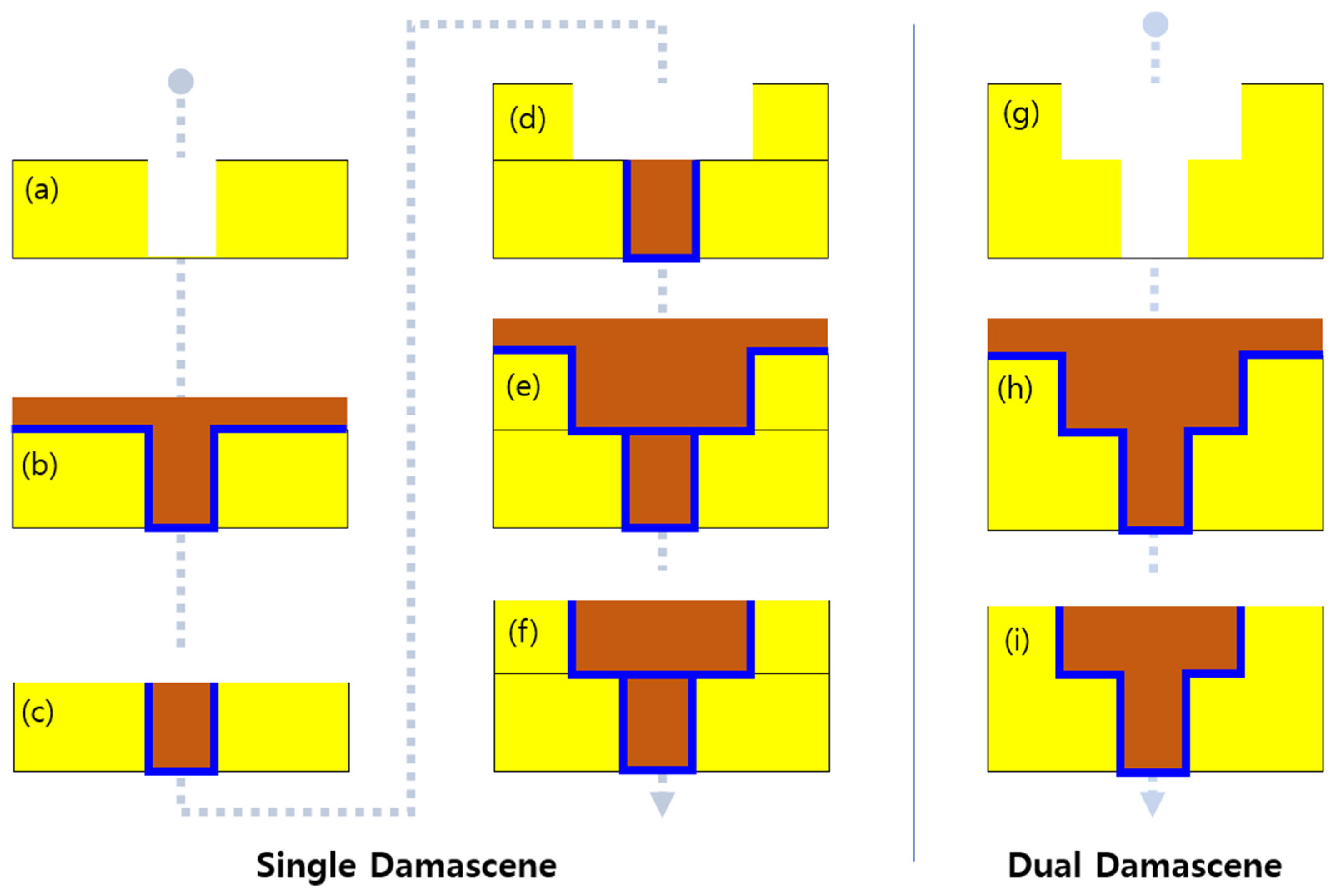
2. Cu Dual-Damascene Interconnects

Unlike Al, Cu cannot be easily patterned using reactive ion etching (RIE) due to the low volatility of CuCl2 and CuF at low temperatures. Due to this constraint, the damascene process was introduced as a replacement for subtractive etching [18,19]. Cu also has reliability issues due to its high diffusivity into the surrounding dielectric material unless it is perfectly encapsulated [20,21,22]. Many studies have sought to resolve the diffusion issue, with tantalum nitride (TaN) mostly employed as a diffusion barrier based on comprehensive comparisons of many candidate materials [23]. IBM announced the first product implementation of a Cu damascene structure in 1997 [7], since which this structure has become the standard platform for on-chip interconnects with improved resistivity and reliability compared with Al interconnects.
In the damascene process, the dielectric is first deposited onto the substrate and then etched to form a metal and via profile. Finally, the incoming profile is filled with Cu metal and the excess Cu removed using chemical mechanical polishing (CMP).
Damascene interconnects have two variations: single-damascene (SD) and dual-damascene (DD) structures. Figure 2 presents a schematic comparison of SD and DD interconnects. The SD process produces the via and the trench separately, while the DD process conducts via and trench patterning separately but their metallization together. Due to the economic advantages of reducing the number of steps in a process, the DD process is widely preferred. However, the SD process is still used for particular purposes such as M1 or with thick metal layers used for global interconnects. SD interconnects are employed for M1 because connection with the CNT module is required, and an SD structure is effective if a thick metal such as an inductor is required.
The DD fabrication process can be divided into via-first and trench-first schemes according to the patterning order. In the trench-first scheme, which was the first DD process, there is no fence between the via and trench, so depositing the seed Cu for electroplating is easy. However, this approach suffers from indirect alignment and a narrower depth of focus for via lithography due to the step height, leading to a non-planar resist. These issues place a restriction on scaling. In contrast, the via-first scheme has a broader lithography processing window, though it is susceptible to plasma damage to the dielectric when employing a porous low-k material. Therefore, DD processing with a metal HM has generally been employed since the 32 nm technology generation [19]. This method effectively combines the advantages of the via-first and trench-first schemes. Figure 3 presents the differences in the plasma damage arising from the via-first and trench-first schemes using a titanium nitride (TiN) metal HM.
Patterned profiles created using the DD process need to be filled using metallization. Cu metallization consists of three steps: barrier/liner deposition, seed Cu deposition, and bulk Cu deposition [12]. Physical vapor deposition (PVD) is employed for the first two steps, while electroplating with additives is used as the standard process for the third. Following metallization, the excess Cu is removed using CMP to produce the final wiring. A dielectric barrier (DB) covers the surface after Cu CMP has been completed. This process is repeated until the final metal is connected to the bonding structure.
The Cu/low-k damascene process has served as a platform for the successful fabrication of BEOL interconnects while satisfying the scaling roadmap over the past 25 years. However, as scaling progresses, patterning, low-k materials, and metallization are all subject to process limitations. The next section summarizes these limitations and describes the approaches that have been proposed to overcome them.

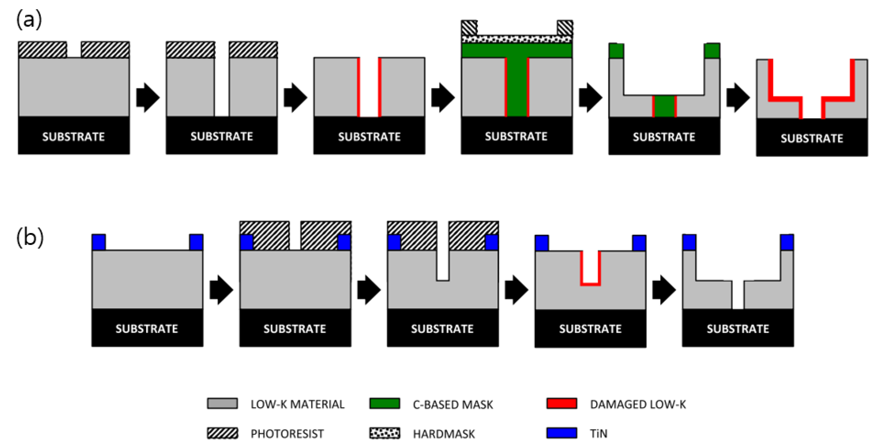
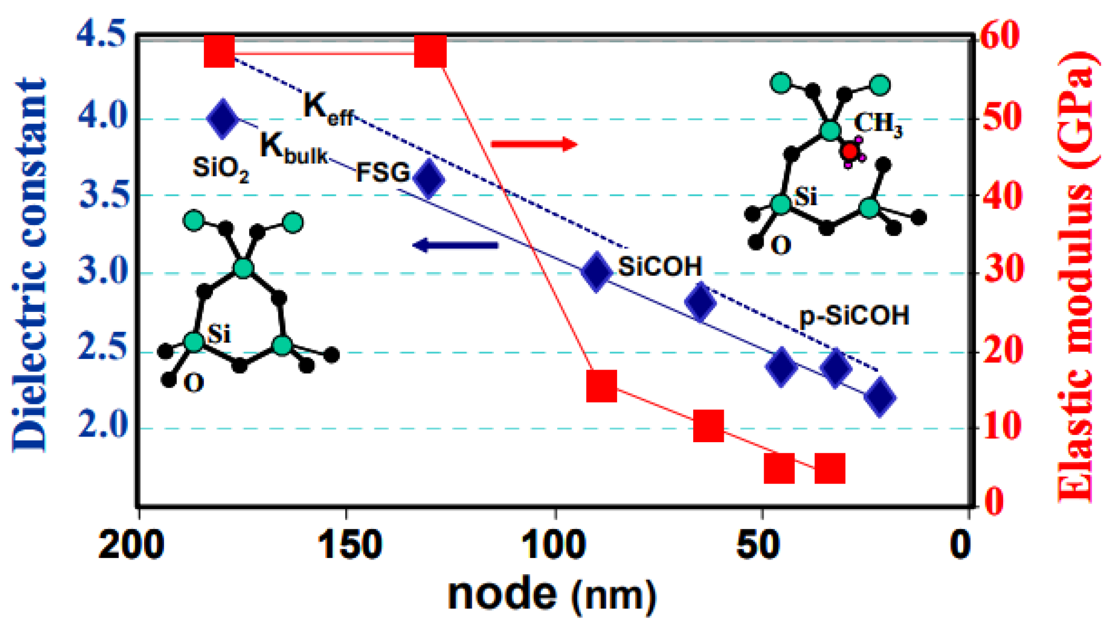
3. Low-k Dielectric Materials

A dielectric material electrically insulates interconnections. When a voltage is applied to an electric wire, the dielectric material induces parasitic capacitance, causing cross-talk noise, power dissipation, and RC delay. These parameters are proportional to the dielectric constant k of the material [8]. However, dielectric materials should not only serve as electrical insulators; they also require reliable mechanical, thermal, chemical, and physical stability under the processing conditions and compatibility with other materials for successful integration [24].
SiO2 is a dielectric material used for 2 to 0.25 μm CMOS technology generations with a dielectric constant of ~4.2. Though SiO2 satisfies the dielectric requirements mentioned above, its k value no longer mitigates the RC delay. Therefore, efforts have been made to find materials with a lower k value that also satisfies the other insulator requirements.
The dielectric constant represents the ratio of the permittivity of a material to that of a vacuum and is generally described using Equation (3) [25]:
k 1 k + 2 = N 3 α  
where k = ε/ε0 and ε and ε0 are the permittivity of the material and vacuum, respectively, N is the number of molecules per unit volume (density), and α is the total polarizability, consisting of electronic (αe) and distortion (αd) polarization.
By decreasing the total polarizability (α) and/or density (N), the k value of the dielectric can be reduced. Density has a more substantial effect on the dielectric constant than does polarizability because density can be reduced to 0 (in an air), leading to k = 1. In the first-generation low-k material obtained using this method, some Si-O bonds were replaced by less polarized Si-F bonds, resulting in FSG [25,26]. In the second generation, a low dielectric constant was achieved using silsesquioxane-based materials and the chemical vapor deposition (CVD) of OSG (SiCOH) [25]. The low dielectric constant of these materials is partially due to the lower density compared with SiO2. The density is reduced by breaking the 3D Si-O-Si bonding network via the incorporation of terminating Si-H or Si-R (where R is an organic moiety such as CH3) [27].
Porosity must also be introduced in order for dense low-k materials to achieve k values below 2.5. This can be accomplished using sacrificial nanoparticles (i.e., porogen) desorbed in a high-temperature baking step, though maintaining a solid matrix structure is essential to avoid weakening the mechanical properties. The resulting material is pSiCOH [8,28]. Table 1 compares the characteristics of low-k materials for each generation.
However, low-k materials with high porosity suffer from lower mechanical strength, lower thermal conductivity, poor adhesion to barriers, plasma damage, and moisture absorption [29]. Figure 4 presents the relationship between mechanical strength and changes in the k value. For FSG, the difference from SiO2 is insignificant in terms of the elastic modulus, but a rapid decrease occurs for dense low-k OSG and pSiCOH.
Unlike low-k inter/intralayer dielectrics (ILDs), low-k DBs offer the integration requirements for downstream manufacturing processes [30]. Low-k DBs are essential components of BEOL interconnects and contribute to their capacitance. This has an increasingly significant impact on technology generations, allowing a decrease in interconnect dimensions. New DBs have a low k value and a low thickness, which reduces the impact on the capacitance of the interconnection and increases reliability concerns. SiN DBs (k~7.0) were replaced by SiCH and SiCNH (k~5.3) caps in 90 nm technology, and thus, the contribution of these DBs to total capacitance has been relatively small in several subsequent technical nodes. However, this contribution has since increased because low-k DBs have not scaled in proportion with the ILDs [8]. In other words, though the thickness of ILDs has decreased every time a new technology node is created, the thickness of low-k DBs cannot decrease at the same rate without degrading the DB characteristics [31,32].
Although low-k dielectrics have been introduced, ensuring a reliable interconnect process under k~2.4 is challenging. However, the use of an air gap is a promising approach to significantly reducing the capacitance because it can achieve an effective dielectric constant below 2.0. Figure 5 presents a cross-sectional image of an air gap.
Although this concept was already known beforehand [33,34,35,36,37], it was first commercially implemented in Intel’s 14 nm technology using an 80 nm pitch multilayer (M4 and M6), with RC benefits of up to 17% [38,39]. In addition, IBM recently suggested the possibility of extending the air gap to the thin-wire level by achieving a capacitance reduction of about 20% compared with the baseline process using an ultra-low-k (ULK) dielectric (k~2.4) [40]. However, air gaps have been limited to selectively applied critical paths.

4. Metallization

A typical DD Cu line is surrounded by a barrier, a liner, and a cap (Figure 6) [41]. The barrier promotes metal adhesion to the dielectric, protects Cu from oxidation, and acts as a nucleation layer for the liner metals. The liner facilitates Cu seeding and the plating process and, more importantly, improves the Cu interface for the suppression of EM. After the emergence of 14 nm technology, a metal cap was applied to the top of the line to improve for EM performance due to the small volume of Cu [42]. A diffusion barrier is required to prevent the Cu from mixing with the surrounding dielectric material when manufacturing a Cu interconnect with a damascene structure. The barrier layer reduces the cross-sectional area of the interconnect, and the effective resistance of the Cu line becomes higher than that of a barrier-free Cu line. The increase in resistivity due to the barrier increases significantly when the width of the interconnect line is reduced. According to Matthiessen’s law, line resistivity consists of bulk resistivity, impurity scattering, surface scattering, and GB scattering [43,44]. Before the emergence of 7 nm technology, bulk resistivity and impurity scattering usually determined line resistivity. However, since then, surface scattering and particle boundary scattering have taken on greater importance. For surface scattering, it is essential to minimize the volume fraction of Cu occupied by the barrier and liner, while particle boundary scattering is likely to affect scattering at the interface and the Cu grain size. This section summarizes important studies reported to date on these issues.

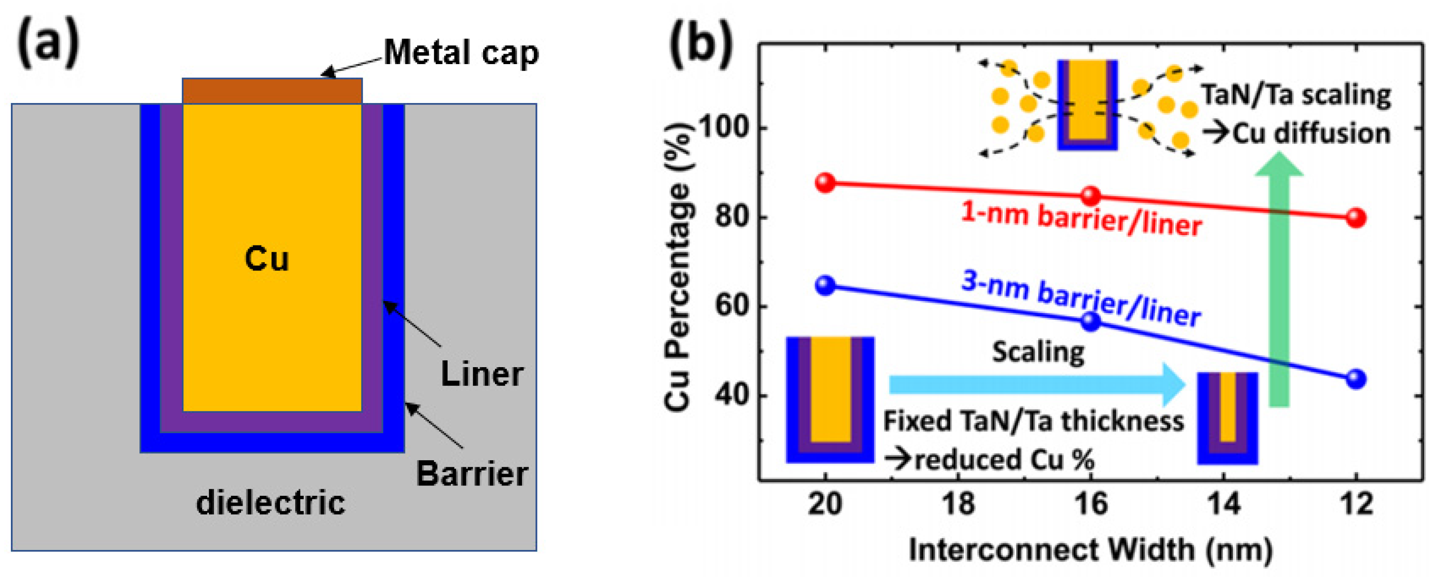
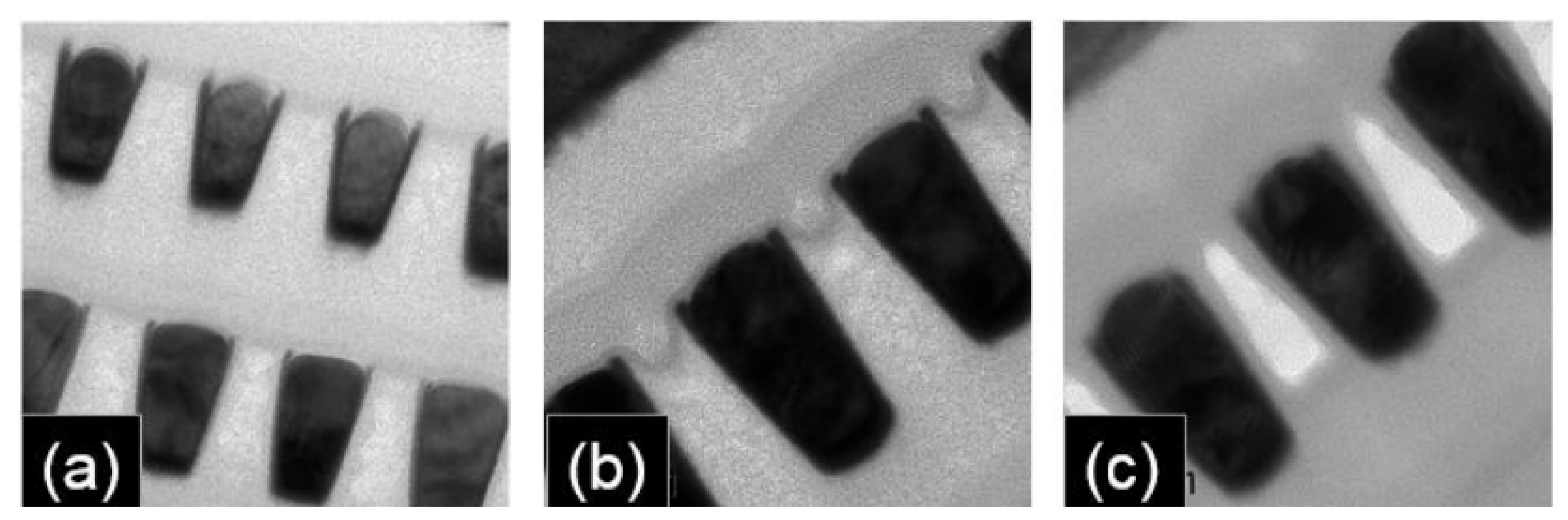
4.1. TaN Barrier/Liner Scaling

In order to maximize the Cu volume fraction, the TaN/Ta liner thickness must be reduced. In addition, the thickness of the Cu seed needs to be reduced to prevent the top pinch-off shape during subsequent Cu electroplating. However, the nonconformal step coverage of PVD results in gap-fill problems caused by the overhang and high resistance due to the thick barrier at the via bottom. Therefore, atomic layer deposition (ALD)/CVD is preferred for maximizing the gap-filling window and minimizing the resistance.
Several approaches have been explored for reducing the TaN barrier thickness. First, the minimum thickness can be reduced without sacrificing TaN barrier properties using PVD [45]. In particular, based on time-dependent dielectric breakdown (TDDB) measurements using a planar capacitor structure, TaN barrier characteristics have been shown to be retained even if the thickness is reduced to as low as 0.8 nm. In addition, it has been reported that using a Co/Ru liner instead of a Ta liner significantly improves the overall integrity of the TaN barrier [45]. However, due to the step coverage limit and the overhang problem associated with PVD, it is necessary to switch to ALD as the dimensions decrease. However, TaN thermally deposited using ALD has a higher number of impurities than PVD-fabricated TaN films, a lower film density, a higher resistance, and a lower interface quality, meaning that it cannot emulate the performance of PVD TaN at the same thickness. For this reason, PVD Ta and ALD TaN have been employed as bilayers (1 nm/1 nm) to reduce the thickness while ensuring the barrier properties [46]. Another approach is treating ALD-fabricated TaN in a PVD chamber to transform it into PVD-like film with optimal density and resistivity [47,48]. Using this method, the TaN thickness is 1.2 nm, compared with 1.5 nm for a Co liner and 2.0 nm for a Ru liner [48]. As a result, ALD has been combined with PVD to maintain the barrier properties and a low TaN thickness.
Scaling of the liner has also been actively carried out. The ALD/CVD method is required to overcome the step coverage and overhang problems, but a Ta liner cannot be used. Therefore, replacements for the Ta liner have been considered. Of these, Ru has received significant attention due to its suitability for ALD/CVD and the possibility of direct Cu plating without a PVD Cu seed layer [49,50,51,52,53,54,55]. In addition, Co has also been considered as a replacement for the Ta liner [56]. In [41], a Ru liner was found to be superior to a Co liner for Cu filling and electroplating with a liner thickness of 2 nm. However, the resistance of Ru was about 10% higher than that of Co as revealed by the temperature coefficient of resistance (TCR), which was believed to be due to interface and GB scattering. A Co liner has also been shown to outperform a Ru liner in terms of EM characteristics [57].
However, in order to fully exploit the excellent void-free gap-fill performance of Ru liners, approaches to improving their EM deficiencies have been reported. Co caps have been established as a standard process since the emergence of 14 nm technology. As a result, a significant improvement in EM performance has been observed with a Ru liner as the Co cap thickness increases [57]. It has also been demonstrated that the EM problem arises from the diffusion of Co from the cap to the liner due to the Co concentration gradient between the two [57,58,59]. Thus, a Co-doped Ru liner has been proposed to overcome this problem, and EM improvements have been reported [58,59]. Efforts to scale the TaN barrier and Co/Ru liner continue, but if the metal half-pitch decreases below 10 nm, the barrier/liner scaling limit is reached.

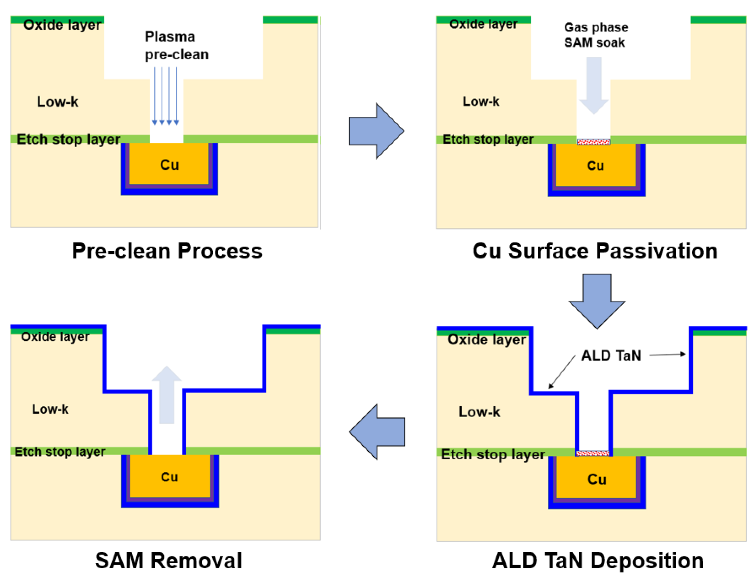
4.2. Selective Barrier Schemes

As advanced technologies emerge, the importance of the resistance and reliability of the vias increases. In particular, via resistance is strongly affected by the bottom thickness of the TaN. Therefore, as scaling progresses, the via resistance rapidly increases due to the thicker TaN. Furthermore, one of the most critical areas of a Cu-based DD structure is the bottom of the via, where the two metal levels meet [60], so selective deposition control of the via bottom barrier is advantageous for improved reliability. In this vein, argon (Ar) sputtering was used as a precleaning PVD barrier/liner [60]. The barrier-first process was conducted in the order of TaN/Ar sputtering/Ta instead of Ar sputtering/TaN/Ta to remove TaN in the via bottom and obtain a Cu/Ta/Cu interface. However, this process disappeared when the precleaning method for removing Cu oxide was changed from Ar sputtering to the oxide-reduction method.
Now that the via size is much smaller, self-assembled monolayers (SAM) have been pursued [61,62]. Figure 7 presents the process for the formation of a selective barrier on the via bottom. The Cu surface is passivated by depositing a SAM on the Cu surface subjected to the CuOx reduction treatment. The SAM should be highly selective and self-limited and be adsorbed onto metals but not other peripheral dielectrics. However, when the SAM attaches to the metal surface, it interferes with the adsorption of ALD TaN precursors, resulting in significant nucleation delays in ALD TaN growth [61,62]. As a result, ALD TaN does not deposit on the via bottom area where the SAM is located. The SAM is finally removed. The SAM process needs to be developed further before it can be adopted for mass production. Nevertheless, because it can achieve a reduction in the via resistance of about 50% and its TDDB and EM results are equivalent to the process of record (POR), it is likely to be useful in future advanced technologies [61].

4.3. Self-Forming Barriers

Another promising approach to Cu extendibility is the through Co self-forming barrier (tCoSFB), a method in which manganese (Mn) atoms added to the seed Cu diffuse through the thin Co liner layer to form a strong diffusion barrier at the interface between the trench and the dielectric, as seen in Figure 8 [63,64,65,66].
Initially, the Mn dopant is employed to form MnSixOy at the dielectric and Cu interface [64,65,67,68]. If CuMn seed deposition occurs without a barrier/liner and Cu plating and annealing are conducted, an SFB is created. This MnSixOy barrier is very thin and uniform, and its EM and TDDB performance is similar to that of POR. However, vertical trench triangular voltage sweep (VT-TVS) and O2 barrier tests indicate that MnSixOy is inadequate for blocking Cu and O2 diffusion, which led to the switch from the SFB to tCoSFB containing thin Ta(N) and Co [69].
The advantage of the tCoSFB process is that the cross-sectional area of Cu in the wiring can be maximized, and low line resistance can be obtained due to the 1 nm thickness of the Co liner and Ta barrier. However, because the line resistance and reliability balance are controlled by the Mn concentration of Cu(Mn) PVD, an increase in resistance may occur. Nevertheless, compared with the POR process, the results are encouraging, with improved resistance and EM and TDDB performance [66,70].

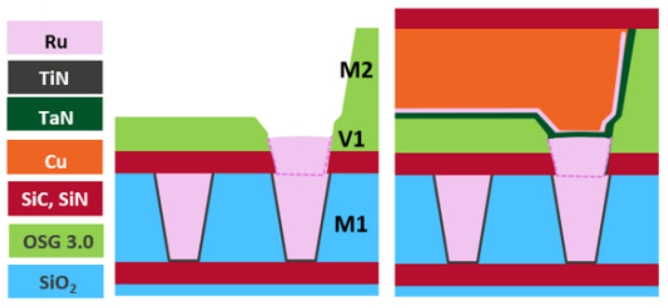
4.4. Hybrid Metallization

At the system-on-chip level, vias have become much more important for signal routing, and via resistance has increased significantly when downscaling the bottom contact area of the via. Therefore, introducing barrierless metal to the via is valuable, and metal−metal selective deposition is essential for the high-aspect-ratio (AR) vias. Hybrid metallization is a method of pre-filling a via with a barrierless metal and then filling the remaining metal area using Cu metallization, as seen in Figure 9 [71].
A barrierless prefill has a number of advantages. First, the prefill moves the barrier position of the Cu DD from the bottom to the top of the via, increasing the tapered via cross-section and reducing the resistance. Second, the gap–fill margin increases because SD trench metallization is employed. Third, because the high-AR vias are excluded, step coverage can be achieved with a thinner barrier/liner [72]. In addition, the optimized barrierless prefilling process may reduce RC delay by increasing the height of the vias and trenches, which can significantly improve circuit performance [73].
The first reported via prefill used Co [73]. However, due to Co ion drift, it was found that barrierless Co was not possible and that TiN barriers are required [72,74]. Ru has been found to be suitable for barrierless prefilling, resulting in a 40% reduction in via resistance and EM results that are similar to those for POR [71].

4.5. Alternative Metals

The thickness of the barrier layer cannot arbitrarily be reduced. If the thickness is less than a certain threshold, it no longer functions as a Cu diffusion barrier. Based on past experimental results, it is unclear whether the barrier/liner combination can have a thickness lower than 2 nm [45,46,47,75]. However, a barrierless solution is required when the half pitch falls below 10 nm, and thus, new metals to replace Cu have been sought. Some of these metals have a larger bulk resistivity than Cu but do not require a thick barrier/liner and exhibit lower resistance at sufficiently small dimensions because their inelastic average free path is shorter than that of Cu (39 nm) [76,77]. Examples of metals and substitutes proposed under these conditions include Ir, Rh, Mo [78], and W [79], but experimentally verified cases are rare except for Co and Ru [80,81,82,83].
Figure 10 displays the line resistance derived from the TCR according to the cross-sectional area of the conductor. Cu has a higher resistance than Ru and Co below ~400 nm2 at a 16-nm metal width and an AR of 2 [84].

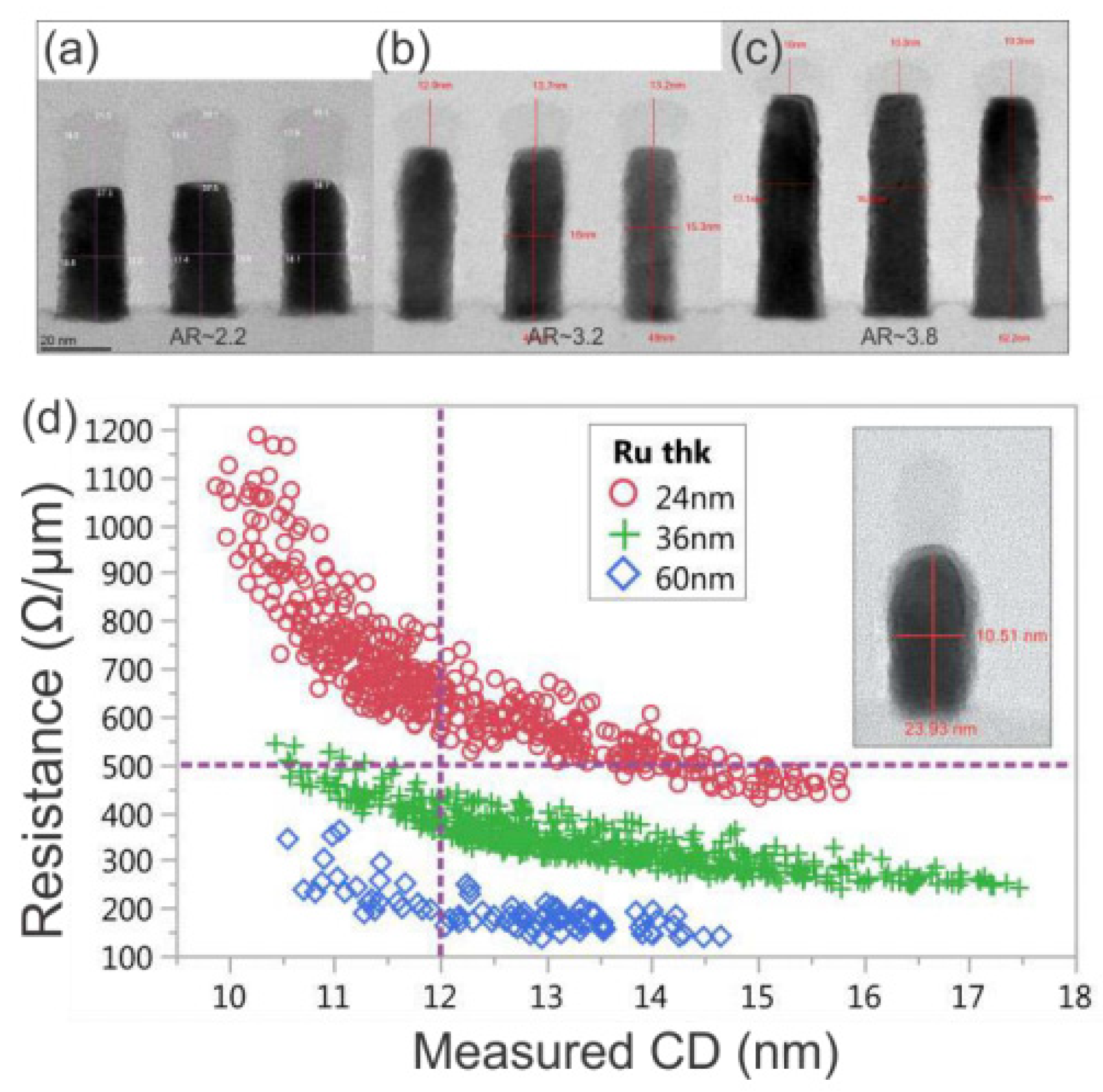
4.6. Ru Semi-Damascene Schemes

Ru can be used in barrierless damascene structures and direct metal etching (DME). Figure 11 shows Ru metal implemented with subtractive etching.
The use of subtractive etching opens up many possibilities that have not previously been possible for Cu damascene structures. First, because the Ru film is deposited on the entire wafer, the grain size is not limited by the damascene profile width. Therefore, it can significantly restrain the increase in resistance due to GB scattering. Second, the metal thickness is determined by Ru deposition, not by metal CMP. Therefore, if necessary, the resistance can be reduced by increasing the Ru thickness, and there is no AR-related filling problem. Third, because the metal thickness is not affected by the pattern density but is determined by the uniformity of the deposited Ru film, the variation in the metal Rs will be reduced. Finally, a space between Ru metal with an increase in the AR could be introduced by employing an intentional air gap.
The semi-damascene process is an interesting approach that utilizes the advantages of Ru, such as barrierless designs and subtractive etching. This method begins with vias fabricated in a low-k material, and the vias and trench layers are filled using a single deposition step. Subtractive etching is then applied to the trench patterning [14,85,86,87]. According to the latest result, Ru line resistance outperforms Cu at 270 nm2 or lower (CD < 12 nm) based on line resistance vs. conducting area plot, and the EM and TDDB results are promising so far [17]. For this reason, the Ru semi-damascene process is the most competitive candidate for use in 3 nm technology and lower.
Figure 12 shows the conceptual summary of the metallization approaches mentioned in this section as they have evolved. As shown in the figure, the main trend of metallization has been to reduce the area ratio occupied by the barrier in the scaled wire. Traditional attempts were to reduce the existing barrier/liner (TaN/Ta) thickness by replacing a new process method (ALD) and a new liner material (Co/Ru). After that, it was gradually developed to implement a barrier-free process using Co or Ru. Moreover, the boundary has recently been extended to the subtraction etch process using Ru instead of the Cu damascene scheme.
In addition to the metallization approaches mentioned here, various studies are being conducted. One of them is the study of a 2D-like barrier. The approach is to minimize the volume fraction of Cu occupied by the barrier by replacing the thick Ta or TaN barrier with 2D-like materials such as graphene [88,89], MoS2 [41,90], TaS2 [41], and WSe2 [41].
In the process of these efforts, the limitation of Cu metallization in CMOS interconnects is becoming more apparent. However, it is interesting that Cu plating is actively applied in other areas, such as solar cells’ silicon heterojunction (SHJ) [91,92].

5. Reliability

Recognizing the underlying causes of reliability problems in scaled Cu/low-k interconnects and clearly understanding the degradation mechanisms are essential. EM and TDDB are standard methods for assessing the reliability of metal and dielectrics. Therefore, EM and TDDB are summarized in this section, and countermeasures proposed for improving reliability in the pursuit of scaling are discussed.

5.1. Electromigration

EM is a phenomenon in which metal atoms move in a metal conductor due to a high current density [93]. When EM stress is continuously applied, voids appear on the cathode side of the wire as the metal atoms accumulate on the anode side, resulting in hydrostatic stress. This stress also produces an inverse flux of atoms in the opposite direction to the electron transport flux, which is referred to as the Blech effect or the short-length effect [94,95]. This back-stress force is more evident as the wire length decreases, preventing EM failure because it prevents the formation of a void when it is shorter than the critical threshold length [94,95].
In a Cu damascene structure, the TaN/Ta barrier and the DB act as a boundary for the Cu, and this is where the depletion of metal atoms begins. As a result, Cu EM shifts into the voids through the nucleation, incubation, and growth phases [96]. The dimensions of the vias and metal determine the likelihood that the voids produced in this manner will affect the resistance. Therefore, early failure initiates near the via bottom, and late failure is observed as a void in the metal line.
EM testing is performed under high-current-density and high-temperature conditions to obtain a failure time for when the resistance increases experimentally. The failure time (t) is widely described using Black’s equation [97]:
t = A j n exp E a k T
where j is the current density, E a   is the activation energy for diffusion, k is the Boltzmann constant, T is the temperature, A is a constant, and n is the current exponent, whose value is typically between 1 and 2.
The activation energy for diffusion depends on the specific metal atoms involved and the diffusion path. Table 2 summarizes the activation energy for Al and Cu, with the diffusion paths divided into bulk, GB, interface, and surface. It is expected that the lower the activation energy, the faster the failure time detection will be.
GB diffusion is the fastest path for Al, while surface diffusion is the fastest path for Cu due to the low activation energy. Therefore, to improve the EM lifetime, it is necessary to improve the paths with the lowest activation energy. For example, for Cu, the surface and interface should be improved first. For the surface diffusion path, strengthening the adhesion between Cu and the DB is the most important goal, with HN3 plasma employed to remove Cu oxidation. CoWP [98] is then added, along with a Co cap [42,99] to maintain EM performance and meet the higher current density requirements of advanced technology generations. Similarly, at the interface, there is an adhesion issue between the liner and Cu. Therefore, EM improvement must be verified when evaluating new materials such as Co and Ru liners and reducing barrier/liner thickness [46,47,57,58,59,75]. For the GBs, the lower the metal width, the more difficult it is to improve the EM because the grain growth is limited by the metal width. However, it has been reported that the grain size increases with a longer annealing time when Cu reflowing is employed, although the result is not yet clear [48]. Finally, there is a method of improving EM by depositing doping impurities together with the seed Cu. Various metals (e.g., Al, Ag, Mn, Mg, and Zr) have been tested in this respect, and Mn is currently the most commonly used. However, the resistance increases as the doping concentration increases, so optimizing EM and resistance are required.

5.2. Time-Dependent Dielectric Breakdown

When long-term stress is applied in a strong electric field, electrical damage occurs to the dielectric material, and insulation is lost, ultimately leading to TDDB [100]. This TDDB has been treated as an essential reliability item in the gate oxide. In the past BEOL interconnects, the size of the electric field applied to the insulator did not become a problem because of the excellent insulation characteristics of SiO2 and sufficient gaps between wirings. However, as scaling progressed, the size of the electric field across the dielectric gradually increased, and porous low-k materials were introduced, leading to TDDB becoming an essential measure of reliability for BEOL interconnects [101]. The breakdown strength of a porous low-k material decreases as the dielectric constant decreases.
The pores in a porous low-k material shorten the percolation paths, weaken the bonds at the metal−insulator interface, and have a high trap density. The interface between the low-k material and the DB is the most problematic in this respect because of the possibility of a high trap density due to CMP, bond mismatches due to material differences, and the shorter distances arising from a tapered morphology [102]. In addition, a breakdown current may be generated by the defects in the porous low-k material in its as-deposited state or following plasma damage received during the fabrication process such as RIE etch.
In addition to these intrinsic causes, Cu metallization also affects TDDB. Cu diffusion into the dielectric may occur through the metal barrier and DB. Thus, TDDB should be evaluated when applying a change in the characteristics or thickness of a new barrier material. Since the TDDB test is performed at a deliberately high acceleration voltage, a TDDB lifetime model is required for predicting the actual lifetime at the standard operating voltage from the TDDB measurement results. E and E1/2 models are widely used as standards for TDDB reliability testing, which is important because they are the most conservative predictors of low-k TDDB [103]. Of these, the E1/2 model is most capable of explaining low-k TDDB behavior due to Cu diffusion.

6. Summary

Because introducing a new dielectric material with a lower k value to microchip interconnects is likely to prove difficult, efforts to suppress the increase in RC delay due to scaling have concentrated on the metallization process. Furthermore, more innovative approaches to metallization are required when the minimum metal pitch required by the process node is less than 40 nm (10 nm technology or lower).
These innovative approaches, as mentioned earlier, are traditionally moving toward implementing a barrier-less method by introducing new materials from an approach that reduces the thickness of the barrier/liner. Moreover, in recent years, due to the limitations of Cu damascene structures, subtractive etching has been employed as a process option. However, no single metallization approach can satisfy all BEOL interconnect levels simultaneously. Therefore, depending on the purpose of each level, maximum chip performance can be achieved by selectively employing the various metallization options.
As the scaling of interconnects continues, it is doubtful that current metallization approaches will continue to satisfy the requirements for minimizing the RC delay. As in the case of low-k materials, it may no longer be practical to pursue the scaling of metallization. Rather, the innovative approaches proposed to date can contribute to scaling requirements not through direct scaling but with architectural innovations such as super vias and buried power rails.

Funding

This work is supported by the “Ling Yan” Program for Tackling Key Problems in Zhejiang Province under Grant number of No. 2022C01098.

Data Availability Statement

No new data were created or analyzed in this study. Data sharing is not applicable to this article.

Conflicts of Interest

The author declares no conflict of interest.

References

  1. Davis, J.A.; Venkatesan, R.; Kaloyeros, A.; Beylansky, M.; Souri, S.; Banerjee, K.; Saraswat, K.; Rahman, A.; Reif, R.; Meindl, J. Interconnect limits on gigascale integration (GSI) in the 21st century. Proc. IEEE 2001, 89, 305–324. [Google Scholar] [CrossRef]
  2. Bonilla, G.; Lanzillo, N.; Hu, C.-K.; Penny, C.; Kumar, A. Interconnect scaling challenges, and opportunities to enable system-level performance beyond 30 nm pitch. In Proceedings of the 2020 IEEE International Electron Devices Meeting (IEDM), San Francisco, CA, USA, 12–18 December 2020. [Google Scholar] [CrossRef]
  3. Theis, T.N. The future of interconnection technology. IBM J. Res. Dev. 2000, 44, 379–390. [Google Scholar] [CrossRef]
  4. Havemann, R.; Hutchby, J. High-performance interconnects: An integration overview. Proc. IEEE 2001, 89, 586–601. [Google Scholar] [CrossRef]
  5. Baccarani, G.; Wordeman, M.; Dennard, R. Generalized scaling theory and its application to a ¼ micrometer MOSFET design. IEEE Trans. Electron Devices 1984, 31, 452–462. [Google Scholar] [CrossRef]
  6. Cheng, Y.-L.; Lee, C.-Y. Porous low-dielectric-constant material for semiconductor microelectronics. In Nanofluid Flow in Porous Media; IntechOpen: London, UK, 2018. [Google Scholar] [CrossRef]
  7. Saito, T.; Imai, T.; Noguchi, J.; Kubo, M.; Ito, Y.; Omori, S.; Ohashi, N.; Tamaru, T.; Yamaguchi, H. A high performance liner for copper damascene interconnects. In Proceedings of the IEEE 2001 International Interconnect Technology Conference (Cat. No. 01EX461), Burlingame, CA, USA, 6 June 2001. [Google Scholar] [CrossRef]
  8. Edelstein, D.; Heidenreich, J.; Goldblatt, R.; Cote, W.; Uzoh, C.; Lustig, N.; Roper, P.; McDevitt, T.; Motsiff, W.; Simon, A.; et al. Full copper wiring in a sub-0.25/spl mu/m CMOS ULSI technology. In Proceedings of the International Electron Devices Meeting. IEDM Technical Digest, Washington, DC, USA, 10 December 1997. [Google Scholar] [CrossRef]
  9. Grill, A.; Gates, S.M.; Ryan, T.E.; Nguyen, S.V.; Priyadarshini, D. Progress in the development and understanding of advanced low k and ultralow k dielectrics for very large-scale integrated interconnects—State of the art. Appl. Phys. Rev. 2014, 1, 011306. [Google Scholar] [CrossRef]
  10. Grill, A. Porous pSiCOH ultralow-k dielectrics for chip interconnects prepared by PECVD. Annu. Rev. Mater. Res. 2009, 39, 49–69. [Google Scholar] [CrossRef]
  11. Lionti, K.; Volksen, W.; Magbitang, T.; Darnon, M.; Dubois, G.; Lyu, Y.-R.; Hsieh, T.-E. Toward successful integration of porous low-k materials: Strategies addressing plasma damage. ECS J. Solid State Sci. Technol. 2014, 4, N3071. [Google Scholar] [CrossRef]
  12. Cheng, Y.-L.; Lee, C.-Y.; Huang, Y.-L. Copper metal for semiconductor interconnects. In Noble and Precious Metals-Properties, Nanoscale Effects and Applications; IntechOpen: London, UK, 2018; pp. 220–221. [Google Scholar] [CrossRef]
  13. Simon, A.; van der Straten, O.; Lanzillo, N.A.; Yang, C.-C.; Nogami, T.; Edelstein, D.C. Role of high aspect-ratio thin-film metal deposition in Cu back-end-of-line technology. J. Vac. Sci. Technol. A Vac. Surf. Film. 2020, 38, 053402. [Google Scholar] [CrossRef]
  14. Croes, K.; Adelmann, C.; Wilson, C.J.; Zahedmanesh, H.; Pedreira, O.V.; Wu, C.; Leśniewska, A.; Oprins, H.; Beyne, S.; Ciofi, I.; et al. Interconnect metals beyond copper: Reliability challenges and opportunities. In Proceedings of the 2018 IEEE International Electron Devices Meeting (IEDM), San Francisco, CA, USA, 1–5 December 2018. [Google Scholar] [CrossRef]
  15. Decoster, S.; Camerotto, E.; Murdoch, G.; Kundu, S.; Le, Q.T.; Tőkei, Z.; Jurczak, G.; Lazzarino, F. Patterning challenges for direct metal etch of ruthenium and molybdenum at 32 nm metal pitch and below. J. Vac. Sci. Technol. B Nanotechnol. Microelectron. Mater. Process. Meas. Phenom. 2022, 40, 032802. [Google Scholar] [CrossRef]
  16. Paolillo, S.; Wan, D.; Lazzarino, F.; Rassoul, N.; Piumi, D.; Tőkei, Z. Direct metal etch of ruthenium for advanced interconnect. J. Vac. Sci. Technol. B Nanotechnol. Microelectron. Mater. Process. Meas. Phenom. 2018, 36, 03E103. [Google Scholar] [CrossRef]
  17. Murdoch, G.; O’Toole, M.; Marti, G.; Pokhrel, A.; Tsvetanova, D.; Decoster, S.; Kundu, S.; Oniki, Y.; Thiam, A.; Le, Q.; et al. First demonstration of Two Metal Level Semi-damascene Interconnects with Fully Self-aligned Vias at 18MP. In Proceedings of the 2022 IEEE Symposium on VLSI Technology and Circuits (VLSI Technology and Circuits), Honolulu, HI, USA, 13–17 June 2022. [Google Scholar] [CrossRef]
  18. Gambino, J.; Chen, F.; He, J. Copper interconnect technology for the 32 nm node and beyond. In Proceedings of the 2009 IEEE Custom Integrated Circuits Conference, San Jose, CA, USA, 13–16 September 2009. [Google Scholar] [CrossRef]
  19. Kriz, J.; Angelkort, C.; Czekalla, M.; Huth, S.; Meinhold, D.; Pohl, A.; Schulte, S.; Thamm, A.; Wallace, S. Overview of dual damascene integration schemes in Cu BEOL integration. Microelectron. Eng. 2008, 85, 2128–2132. [Google Scholar] [CrossRef]
  20. Lloyd, J.; Murray, C.; Ponoth, S.; Cohen, S.; Liniger, E. The effect of Cu diffusion on the TDDB behavior in a low-k interlevel dielectrics. Microelectron. Reliab. 2006, 46, 1643–1647. [Google Scholar] [CrossRef]
  21. Tsu, R.; McPherson, J.W.; McKee, W.R. Leakage and breakdown reliability issues associated with low-k dielectrics in a dual-damascene Cu process. In Proceedings of the 2000 IEEE International Reliability Physics Symposium Proceedings 38th Annual (Cat. No. 00CH37059), San Jose, CA, USA, 10–13 April 2000. [Google Scholar] [CrossRef]
  22. McPherson, J.W. Time dependent dielectric breakdown in copper low-k interconnects: Mechanisms and reliability models. Materials 2012, 5, 1602–1625. [Google Scholar] [CrossRef]
  23. Edelstein, D.; Uzoh, C.; Cabral, C.; DeHaven, P.; Buchwalter, P.; Simon, A.; Cooney, E.; Malhotra, S.; Klaus, D.; Rathore, H.; et al. A high performance liner for copper damascene interconnects. In Proceedings of the IEEE 2001 International Interconnect Technology Conference (Cat. No. 01EX461), Burlingame, CA, USA, 6 June 2001. [Google Scholar] [CrossRef]
  24. Shamiryan, D.; Abell, T.; Iacopi, F.; Maex, K. Low-k dielectric materials. Mater. Today 2004, 7, 34–39. [Google Scholar] [CrossRef]
  25. Maex, K.; Baklanov, M.R.; Shamiryan, D.; Lacopi, F.; Brongersma, S.H.; Yanovitskaya, Z.S. Low dielectric constant materials for microelectronics. J. Appl. Phys. 2003, 93, 8793–8841. [Google Scholar] [CrossRef]
  26. Cheng, Y.; Wang, Y.; Liu, C.; Wu, Y.; Lo, K.; Lan, J. Characterization and reliability of low dielectric constant fluorosilicate glass and silicon rich oxide process for deep sub-micron device application. Thin Solid Films 2001, 398, 533–538. [Google Scholar] [CrossRef]
  27. Hoofman, R.; Verheijden, G.; Michelon, J.; Iacopi, F.; Travaly, Y.; Baklanov, M.; Tökei, Z.; Beyer, G. Challenges in the implementation of low-k dielectrics in the back-end of line. Microelectron. Eng. 2005, 80, 337–344. [Google Scholar] [CrossRef]
  28. Sankaran, S.; Arai, S.; Augur, R.; Beck, M.; Biery, G.; Bolom, T.; Bonilla, G.; Bravo, O.; Chanda, K.; Chae, M.; et al. A 45 nm CMOS node Cu/Low-k/Ultra Low-k PECVD SiCOH (k = 2.4) BEOL technology. In Proceedings of the 2006 International Electron Devices Meeting, San Francisco, CA, USA, 11–13 December 2006. [Google Scholar] [CrossRef]
  29. Travaly, Y.; van Aelst, J.; Truffert, V.; Verdonck, P.; Dupont, T.; Camerotto, E.; Richard, O.; Bender, H.; Kroes, C.; de Roest, D.; et al. Key factors to sustain the extension of a MHM-based integration scheme to medium and high porosity PECVD low-k materials. In Proceedings of the 2008 International Interconnect Technology Conference, Burlingame, CA, USA, 1–4 June 2008. [Google Scholar] [CrossRef]
  30. King, S.W. Dielectric barrier, etch stop, and metal capping materials for state of the art and beyond metal interconnects. ECS J. Solid State Sci. Technol. 2014, 4, N3029. [Google Scholar] [CrossRef]
  31. Cheng, Y.-L.; Chen, S.-A.; Chiu, T.-J.; Wu, J.; Wei, B.-J.; Chang, H.-J. Electrical and reliability performances of nitrogen-incorporated silicon carbide dielectric by chemical vapor deposition. J. Vac. Sci. Technol. B Nanotechnol. Microelectron. Mater. Process. Meas. Phenom. 2010, 28, 573–576. [Google Scholar] [CrossRef]
  32. Cheng, Y.-L.; Chiu, T.-J.; Wei, B.-J.; Wang, H.-J.; Wu, J.; Wang, Y.-L. Effect of copper barrier dielectric deposition process on characterization of copper interconnect. J. Vac. Sci. Technol. B Nanotechnol. Microelectron. Mater. Process. Meas. Phenom. 2010, 28, 567–572. [Google Scholar] [CrossRef]
  33. Nitta, S.; Edelstein, D.; Ponoth, S.; Clevenger, L.; Liu, X.; Standaert, T. Performance and reliability of airgaps for advanced BEOL interconnects. In Proceedings of the 2008 International Interconnect Technology Conference, Burlingame, CA, USA, 1–4 June 2008. [Google Scholar] [CrossRef]
  34. Chen, H.-W.; Jeng, S.-P.; Tsai, H.-Y.; Liu, Y.-W.; Yu, C.; Sun, Y. A self-aligned air gap interconnect process. In Proceedings of the 2008 International Interconnect Technology Conference, Burlingame, CA, USA, 1–4 June 2008. [Google Scholar] [CrossRef]
  35. Nakamura, N.; Matsunaga, N.; Kaminatsui, T.; Watanabe, K.; Shibata, H. Cost-effective air-gap interconnects by all-in-one post-removing process. In Proceedings of the 2008 International Interconnect Technology Conference, Burlingame, CA, USA, 1–4 June 2008. [Google Scholar] [CrossRef]
  36. Uno, S.; Noguchi, J.; Ashihara, H.; Oshima, T.; Sato, K.; Konishi, N.; Saito, T.; Hara, K. Dual damascene process for air-gap Cu interconnects using conventional CVD films as sacrificial layers. In Proceedings of the IEEE 2005 International Interconnect Technology Conference, Burlingame, CA, USA, 6–8 June 2005. [Google Scholar] [CrossRef]
  37. Noguchi, J.; Sato, K.; Konishi, N.; Uno, S.; Oshima, T.; Ishikawa, K.; Ashihara, H.; Saito, T.; Kubo, M.; Tamaru, T.; et al. Process and reliability of air-gap Cu interconnect using 90-nm node technology. IEEE Trans. Electron Devices 2005, 52, 352–359. [Google Scholar] [CrossRef]
  38. Fischer, K.; Agostinelli, M.; Allen, C.; Bahr, D.; Bost, M.; Charvat, P.; Chikarmane, V.; Fu, Q.; Ganpule, C.; Haran, M.; et al. Low-k interconnect stack with multi-layer air gap and tri-metal-insulator-metal capacitors for 14nm high volume manufacturing. In Proceedings of the 2015 IEEE International Interconnect Technology Conference and 2015 IEEE Materials for Advanced Metallization Conference (IITC/MAM), Grenoble, France, 18–21 May 2015. [Google Scholar] [CrossRef]
  39. Fischer, K.; Chang, H.; Ingerly, D.; Jin, I.; Kilambi, H.; Longun, J.; Patel, R.; Pelto, C.; Petersburg, C.; Plekhanov, P.; et al. Performance enhancement for 14nm high volume manufacturing microprocessor and system on a chip processes. In Proceedings of the 2016 IEEE International Interconnect Technology Conference/Advanced Metallization Conference (IITC/AMC), San Jose, CA, USA, 23–26 May 2016. [Google Scholar] [CrossRef]
  40. Penny, C.; Gates, S.; Peethala, B.; Lee, J.; Priyadarshini, D.; Nguyen, S.; McLaughlin, P.; Liniger, E.; Hu, C.-K.; Clevenger, L.; et al. Reliable airgap BEOL technology in advanced 48 nm pitch copper/ULK interconnects for substantial power and performance benefits. In Proceedings of the 2017 IEEE International Interconnect Technology Conference (IITC), Hsinchu, Taiwan, 16–18 May 2017. [Google Scholar] [CrossRef]
  41. Lo, C.-L.; Helfrecht, B.A.; He, Y.; Guzman, D.M.; Onofrio, N.; Zhang, S.; Weinstein, D.; Strachan, A.; Chen, Z. Opportunities and challenges of 2D materials in back-end-of-line interconnect scaling. J. Appl. Phys. 2020, 128, 080903. [Google Scholar] [CrossRef]
  42. Chang, S.Y.; Wan, C.C.; Wang, Y.Y. Selectivity enhancement of electroless Co deposition for Cu capping process via spontaneous diazonium ion reduction. Electrochem. Solid-State Lett. 2007, 10, D43. [Google Scholar] [CrossRef]
  43. Shimada, M.; Moriyama, M.; Ito, K.; Tsukimoto, S.; Murakami, M. Electrical resistivity of polycrystalline Cu interconnects with nano-scale linewidth. J. Vac. Sci. Technol. B Microelectron. Nanometer Struct. Process. Meas. Phenom. 2006, 24, 190–194. [Google Scholar] [CrossRef]
  44. Steinhögl, W.; Schindler, G.; Steinlesberger, G.; Engelhardt, M. Size-dependent resistivity of metallic wires in the mesoscopic range. Phys. Rev. B 2002, 66, 075414. [Google Scholar] [CrossRef]
  45. Witt, C.; Yeap, K.; Lesniewska, A.; Wan, D.; Jordan, N.; Ciofi, I.; Wu, C.; Tokei, Z. Testing the limits of TaN barrier scaling. In Proceedings of the 2018 IEEE International Interconnect Technology Conference (IITC), Santa Clara, CA, USA, 4–7 June 2018. [Google Scholar] [CrossRef]
  46. Motoyama, K.; van der Straten, O.; Maniscalco, J.; Huang, H.; Kim, Y.; Choi, J.; Lee, J.; Hu, C.-K.; McLaughlin, P.; Standaert, T.; et al. Ru liner scaling with ALD TaN barrier process for low resistance 7 nm Cu interconnects and beyond. In Proceedings of the 2018 IEEE International Interconnect Technology Conference (IITC), Santa Clara, CA, USA, 4–7 June 2018. [Google Scholar] [CrossRef]
  47. Wu, Z.; Li, R.; Xie, X.; Suen, W.; Tseng, J.; Bekiaris, N.; Vinnakota, R.; Kashefizadeh, K.; Naik, M. PVD-treated ALD TaN for Cu interconnect extension to 5 nm node and beyond. In Proceedings of the 2018 IEEE International Interconnect Technology Conference (IITC), Santa Clara, CA, USA, 4–7 June 2018. [Google Scholar] [CrossRef]
  48. Bhosale, P.S.; Maniscalco, J.; Lanzillo, N.; Nogami, T.; Canaperi, D.; Motoyama, K.; Huang, H.; McLaughlin, P.; Shaviv, R.; Stolfi, M.; et al. Modified ALD TaN barrier with Ru liner and dynamic Cu reflow for 36nm pitch interconnect integration. In Proceedings of the 2018 IEEE International Interconnect Technology Conference (IITC), Santa Clara, CA, USA, 4–7 June 2018. [Google Scholar] [CrossRef]
  49. Yang, C.-C.; Spooner, T.; Ponoth, S.; Chanda, K.; Simon, A.; Lavoie, C.; Lane, M.; Hu, C.-K.; Liniger, E.; Gignac, L.; et al. Physical, electrical, and reliability characterization of Ru for Cu interconnects. In Proceedings of the 2006 International Interconnect Technology Conference, Burlingame, CA, USA, 5–7 June 2006. [Google Scholar] [CrossRef]
  50. Abe, M.; Ueki, M.; Tada, M.; Onodera, T.; Furutake, N.; Shimura, K.; Saito, S.; Hayashi, Y. Highly-oriented PVD ruthenium liner for low-resistance direct-plated Cu interconnects. In Proceedings of the 2007 IEEE International Interconnect Technology Conference, Burlingame, CA, USA, 4–6 June 2007. [Google Scholar] [CrossRef]
  51. Mori, K.; Ohmori, K.; Torazawa, N.; Hirao, S.; Kaneyama, S.; Korogi, H.; Maekawa, K.; Fukui, S.; Tomita, K.; Inoue, M.; et al. Effects of Ru-Ta alloy barrier on Cu filling and reliability for Cu interconnects. In Proceedings of the 2008 International Interconnect Technology Conference, Burlingame, CA, USA, 1–4 June 2008. [Google Scholar] [CrossRef]
  52. Huang, H.Y.; Hsieh, C.H.; Jeng, S.M.; Tao, H.J.; Cao, M.; Mii, Y.J. A new enhancement layer to improve copper interconnect performance. In Proceedings of the 2010 IEEE International Interconnect Technology Conference, Burlingame, CA, USA, 6–9 June 2010. [Google Scholar] [CrossRef]
  53. Rullan, J.; Ishizaka, T.; Cerio, F.; Mizuno, S.; Mizusawa, Y.; Ponnuswamy, T.; Reid, J.; McKerrow, A.; Yang, C.-C. Low resistance wiring and 2Xnm void free fill with CVD Ruthenium liner and DirectSeed TM copper. In Proceedings of the 2010 IEEE International Interconnect Technology Conference, Burlingame, CA, USA, 6–9 June 2010. [Google Scholar] [CrossRef]
  54. Yang, C.-C.; Cohen, S.; Shaw, T.; Wang, P.-C.; Nogami, T.; Edelstein, D. Characterization of “Ultrathin-Cu”/Ru (Ta)/TaN liner stack for copper interconnects. IEEE Electron Device Lett. 2010, 31, 722–724. [Google Scholar] [CrossRef]
  55. Swerts, J.; Armini, S.; Carbonell, L.; Delabie, A.; Franquet, A.; Mertens, S.; Popovici, M.; Schaekers, M.; Witters, T.; Tökei, Z.; et al. Scalability of plasma enhanced atomic layer deposited ruthenium films for interconnect applications. J. Vac. Sci. Technol. A Vac. Surf. Film. 2012, 30, 01A103. [Google Scholar] [CrossRef]
  56. He, M.; Zhang, X.; Nogami, T.; Lin, X.; Kelly, J.; Kim, H.; Spooner, T.; Edelstein, D.; Zhao, L. Mechanism of Co liner as enhancement layer for Cu interconnect gap-fill. J. Electrochem. Soc. 2013, 160, D3040. [Google Scholar] [CrossRef]
  57. Wu, Z.; Chen, F.; Shen, G.; Hu, Y.; Pethe, S.; Lee, J.J.; Tseng, J.; Suen, W.; Vinnakota, R.; Kashefizadeh, K.; et al. Pathfinding of Ru-Liner/Cu-Reflow Interconnect Reliability Solution. In Proceedings of the 2018 IEEE International Interconnect Technology Conference (IITC), Santa Clara, CA, USA, 4–7 June 2018. [Google Scholar] [CrossRef]
  58. Motoyama, K.; van der Straten, O.; Maniscalco, J.; Cheng, K.; DeVries, S.; Huang, H.; Shen, T.; Lanzillo, N.; Hosadurga, S.; Park, K.; et al. Co-doped Ru liners for highly reliable Cu interconnects with selective Co cap. In Proceedings of the 2020 IEEE International Interconnect Technology Conference (IITC), San Jose, CA, USA, 5–8 October 2020. [Google Scholar] [CrossRef]
  59. Motoyama, K. EM performance improvements for Cu interconnects with Ru-based liner and Co cap in advanced nodes. In Proceedings of the 2021 IEEE International Interconnect Technology Conference (IITC), Kyoto, Japan, 6–9 July 2021. [Google Scholar] [CrossRef]
  60. Alers, G.; Rozbicki, R.T.; Harm, G.J.; Kailasam, S.; Ray, G.W.; Danek, M. Barrier-first integration for improved reliability in copper dual damascene interconnects. In Proceedings of the IEEE 2003 International Interconnect Technology Conference (Cat. No. 03TH8695), Burlingame, CA, USA, 4 June 2003. [Google Scholar] [CrossRef]
  61. You, S.; Ren, H.; Naik, M.; Chen, L.; Chen, F.; Cervantes, C.L.; Xie, X.; Kashefizadeh, K. Selective Barrier for Cu Interconnect Extension in 3nm Node and Beyond. In Proceedings of the 2021 IEEE International Interconnect Technology Conference (IITC), Kyoto, Japan, 6–9 July 2021. [Google Scholar] [CrossRef]
  62. Kawasaki, H.; Iwashita, M.; Warashina, H.; Nagai, H.; Iwai, K.; Komatsu, H.; Ozaki, Y.; Pattanaik, G. Advanced Damascene integration using selective deposition of barrier metal with Self Assemble Monolayer. In Proceedings of the 2021 IEEE International Interconnect Technology Conference (IITC), Kyoto, Japan, 6–9 July 2021. [Google Scholar] [CrossRef]
  63. Nogami, T.; Briggs, B.D.; Korkmaz, S.; Chae, M.; Penny, C.; Li, J.; Wang, W.; McLaughlin, P.S.; Kane, T.; Parks, C.; et al. Through-Cobalt Self Forming Barrier (tCoSFB) for Cu/ULK BEOL: A novel concept for advanced technology nodes. In Proceedings of the 2015 IEEE International Electron Devices Meeting (IEDM), Washington, DC, USA, 7–9 December 2015. [Google Scholar] [CrossRef]
  64. Koike, J.; Haneda, M.; Iijima, J.; Wada, M. Cu alloy metallization for self-forming barrier process. In Proceedings of the 2006 International Interconnect Technology Conference, Burlingame, CA, USA, 5–7 June 2006. [Google Scholar] [CrossRef]
  65. Siew, Y.K.; Jourdan, N.; Ciofi, I.; Croes, K.; Wilson, C.J.; Tang, B.J.; Demuynck, S.; Wu, Z.; Ai, H.; Cellier, D.; et al. Cu wire resistance improvement using mn-based self-formed barriers. In Proceedings of the IEEE International Interconnect Technology Conference, San Jose, CA, USA, 20–23 May 2014. [Google Scholar] [CrossRef]
  66. Nogami, T.; Zhang, X.; Kelly, J.; Briggs, B.; You, H.; Patlolla, R.; Huang, H.; McLaughlin, P.; Lee, J.; Shobha, H.; et al. Comparison of key fine-line BEOL metallization schemes for beyond 7 nm node. In Proceedings of the 2017 Symposium on VLSI Technology, Kyoto, Japan, 5–8 June 2017. [Google Scholar] [CrossRef]
  67. Usui, T.; Nasu, H.; Koike, J.; Wada, M.; Takahashi, S.; Shimizu, N.; Nishikawa, T.; Yoshimaru, A.; Shibata, H. Low resistive and highly reliable Cu dual-damascene interconnect technology using self-formed MnSi/sub x/O/sub y/barrier layer. In Proceedings of the IEEE 2005 International Interconnect Technology Conference, Burlingame, CA, USA, 6–8 June 2005. [Google Scholar] [CrossRef]
  68. Usui, T.; Tsumura, K.; Nasu, H.; Hayashi, Y.; Minamihaba, G.; Toyoda, H.; Sawada, H.; Ito, S.; Miyajima, H.; Watanabe, K.; et al. High performance ultra low-k (k = 2.0/keff = 2.4)/Cu dual-damascene interconnect technology with self-formed MnSixOy barrier layer for 32 nm-node. In Proceedings of the 2006 International Interconnect Technology Conference, Burlingame, CA, USA, 5–7 June 2006. [Google Scholar] [CrossRef]
  69. Nogami, T.; Chae, M.; Penny, C.; Shaw, T.; Shobha, H.; Li, J.; Cohen, S.; Hu, C.-K.; Zhang, X.; He, M.; et al. Performance of ultrathin alternative diffusion barrier metals for next-Generation BEOL technologies, and their effects on reliability. In Proceedings of the IEEE International Interconnect Technology Conference., San Jose, CA, USA, 20–23 May 2014. [Google Scholar] [CrossRef]
  70. Nogami, T.; Huang, H.; Shobha, H.; Patlolla, R.; Kelly, J.; Penny, C.; Hu, C.-K.; Sil, D.; Devries, S.; Lee, J.; et al. Technology challenges and enablers to extend Cu metallization to beyond 7 nm node. In Proceedings of the 2019 Symposium on VLSI Technology, Kyoto, Japan, 9–14 June 2019. [Google Scholar] [CrossRef]
  71. van der Veen, M.H.; Soethoudt, J.; Delabie, A.; Pedreira, O.V.; Gonzalez, V.V.; Lariviere, S.; Teugels, L.; Jourdan, N.; Decoster, S.; Struyf, H.; et al. Hybrid Metallization with Cu in sub 30nm Interconnects. In Proceedings of the 2020 IEEE International Interconnect Technology Conference (IITC), San Jose, CA, USA, 5–8 October 2020. [Google Scholar] [CrossRef]
  72. van der Veen, M.H.; Vandersmissen, K.; Dictus, D.; Demuynck, S.; Liu, R.; Bin, X.; Nalla, P.; Lesniewska, A.; Hall, L.; Croes, K.; et al. Cobalt bottom-up contact and via prefill enabling advanced logic and DRAM technologies. In Proceedings of the 2015 IEEE International Interconnect Technology Conference and 2015 IEEE Materials for Advanced Metallization Conference (IITC/MAM), Grenoble, France, 18–21 May 2015. [Google Scholar] [CrossRef]
  73. Zheng, J.-F.; Chen, P.; Baum, T.H.; Lieten, R.R.; Hunks, W.; Lippy, S.; Frye, A.; Li, W.; O'Neill, J.; Xu, J.; et al. Selective Co growth on Cu for void-free via fill. In Proceedings of the 2015 IEEE International Interconnect Technology Conference and 2015 IEEE Materials for Advanced Metallization Conference (IITC/MAM), Grenoble, France, 18–21 May 2015. [Google Scholar] [CrossRef]
  74. Steinhögl, W.; Schindler, G.; Steinlesberger, G.; Traving, M.; Engelhardt, M. Comprehensive study of the resistivity of copper wires with lateral dimensions of 100 nm and smaller. J. Appl. Phys. 2005, 97, 023706. [Google Scholar] [CrossRef]
  75. Lanzillo, N.A.; Yang, C.-C.; Motoyama, K.; Huang, H.; Cheng, K.; Maniscalco, J.; Van Der Straten, O.; Penny, C.; Standaert, T.; Choi, K. Exploring the limits of cobalt liner thickness in advanced copper interconnects. IEEE Electron Device Lett. 2019, 40, 1804–1807. [Google Scholar] [CrossRef]
  76. Hu, C.-K.; Kelly, J.; Chen, J.H.-C.; Huang, H.; Ostrovski, Y.; Patlolla, R.; Peethala, B.; Adusumilli, P.; Spooner, T.; Gignac, L.M.; et al. Electromigration and resistivity in on-chip Cu, Co and Ru damascene nanowires. In Proceedings of the 2017 IEEE International Interconnect Technology Conference (IITC), Hsinchu, Taiwan, 16–18 May 2017; pp. 1–3. [Google Scholar] [CrossRef]
  77. Bekiaris, N.; Wu, Z.; Ren, H.; Naik, M.; Park, J.H.; Lee, M.; Ha, T.H.; Hou, W.; Bakke, J.R.; Gage, M.; et al. Cobalt fill for advanced interconnects. In Proceedings of the 2017 IEEE International Interconnect Technology Conference (IITC), Hsinchu, Taiwan, 16–18 May 2017. [Google Scholar] [CrossRef]
  78. Tierno, D.; Hosseini, M.; van der Veen, M.; Dangol, A.; Croes, K.; Demuynck, S.; Tokei, Z.; Litta, E.; Horiguchi, N. Reliability of Barrierless PVD Mo. In Proceedings of the 2021 IEEE International Interconnect Technology Conference (IITC), Kyoto, Japan, 6–9 July 2021. [Google Scholar] [CrossRef]
  79. Choi, D.; Barmak, K. On the potential of tungsten as next-generation semiconductor interconnects. Electron. Mater. Lett. 2017, 13, 449–456. [Google Scholar] [CrossRef]
  80. Wen, L.G.; Roussel, P.; Pedreira, O.V.; Briggs, B.; Groven, B.; Dutta, S.; Popovici, M.I.; Heylen, N.; Ciofi, I.; Vanstreels, K.; et al. Atomic layer deposition of ruthenium with TiN interface for sub-10 nm advanced interconnects beyond copper. ACS Appl. Mater. Interfaces 2016, 8, 26119–26125. [Google Scholar] [CrossRef] [PubMed]
  81. Zhang, X.; Huang, H.; Patlolla, R.; Wang, W.; Mont, F.W.; Li, J.; Hu, C.-K.; Liniger, E.G.; McLaughlin, P.S.; Labelle, C.; et al. Ruthenium interconnect resistivity and reliability at 48 nm pitch. In Proceedings of the 2016 IEEE International Interconnect Technology Conference/Advanced Metallization Conference (IITC/AMC). San Jose, CA, USA, 23–26 May 2016. [Google Scholar] [CrossRef]
  82. Nogami, T.; Patlolla, R.; Kelly, J.; Briggs, B.; Huang, H.; Demarest, J.; Li, J.; Hengstebeck, R.; Zhang, X.; Lian, G.; et al. Cobalt/copper composite interconnects for line resistance reduction in both fine and wide lines. In Proceedings of the 2017 IEEE International Interconnect Technology Conference (IITC), Hsinchu, Taiwan, 16–18 May 2017. [Google Scholar] [CrossRef]
  83. Dutta, S.; Kundu, S.; Gupta, A.; Jamieson, G.; Granados, J.F.G.; Bommels, J.; Wilson, C.J.; Tokei, Z.; Adelmann, C. Highly scaled ruthenium interconnects. IEEE Electron Device Lett. 2017, 38, 949–951. [Google Scholar] [CrossRef]
  84. van der Veen, M.H.; Heyler, N.; Pedreira, O.V.; Ciofi, I.; Decoster, S.; Gonzalez, V.V.; Jourdan, N.; Struyf, H.; Croes, K.; Wilson, C.J.; et al. Damascene benchmark of Ru, Co and Cu in scaled dimensions. In Proceedings of the 2018 IEEE International Interconnect Technology Conference (IITC), Santa Clara, CA, USA, 4–7 June 2018. [Google Scholar] [CrossRef]
  85. Wan, D.; Paolillo, S.; Rassoul, N.; Kotowska, B.K.; Blanco, V.; Adelmann, C.; Lazzarino, F.; Ercken, M.; Murdoch, G.; Bommels, J.; et al. Subtractive etch of ruthenium for sub-5nm interconnect. In Proceedings of the 2018 IEEE International Interconnect Technology Conference (IITC), Santa Clara, CA, USA, 4–7 June 2018. [Google Scholar] [CrossRef]
  86. Murdoch, G.; Tokei, Z.; Paolillo, S.; Pedreira, O.V.; Vanstreels, K.; Wilson, C.J. Semidamascene Interconnects for 2nm node and Beyond. In Proceedings of the 2020 IEEE International Interconnect Technology Conference (IITC), San Jose, CA, USA, 5–8 October 2020. [Google Scholar] [CrossRef]
  87. Lesniewska, A.; Roussel, P.; Tierno, D.; Gonzalez, V.V.; van der Veen, M.H.; Verdonck, P.; Jourdan, N.; Wilson, C.; Tokei, Z.; Croes, K. Dielectric reliability study of 21 nm pitch interconnects with barrierless Ru fill. In Proceedings of the 2020 IEEE International Reliability Physics Symposium (IRPS), Dallas, TX, USA, 28 April–30 May 2020. [Google Scholar] [CrossRef]
  88. Son, M.; Jang, J.; Lee, Y.; Nam, J.; Hwang, J.Y.; Kim, I.S.; Lee, B.H.; Ham, M.-H.; Chee, S.-S. Copper-graphene heterostructure for back-end-of-line compatible high-performance interconnects. NPJ 2D Mater. Appl. 2021, 5, 41. [Google Scholar] [CrossRef]
  89. Nogami, T.; Nguyen, S.; Huang, H.; Lanzillo, N.; Shobha, H.; Li, J.; Peethela, B.; Parbatani, A.; van Schravendijk, B.; Varadarajan, B.; et al. Electromigration and line R of graphene capped Cu dual Damascene interconnect. In Proceedings of the 2021 IEEE International Electron Devices Meeting (IEDM), San Francisco, CA, USA, 11–16 December 2021. [Google Scholar] [CrossRef]
  90. Lo, C.-L.; Zhang, K.; Smith, R.S.; Shah, K.; Robinson, J.A.; Chen, Z. Large-area, single-layer molybdenum disulfide synthesized at BEOL compatible temperature as Cu diffusion barrier. IEEE Electron Device Lett. 2018, 39, 873–876. [Google Scholar] [CrossRef]
  91. Yu, J.; Li, J.; Zhao, Y.; Lambertz, A.; Chen, T.; Duan, W.; Liu, W.; Yang, X.; Huang, Y.; Ding, K. Copper metallization of electrodes for silicon heterojunction solar cells: Process, reliability and challenges. Sol. Energy Mater. Sol. Cells 2021, 224, 110993. [Google Scholar] [CrossRef]
  92. Yang, L.; Zhong, S.; Zhang, W.; Li, X.; Li, Z.; Zhuang, Y.; Wang, X.; Zhao, L.; Cao, X.; Deng, X.; et al. Study and development of rear-emitter Si heterojunction solar cells and application of direct copper metallization. Prog. Photovolt. Res. Appl. 2018, 26, 385–396. [Google Scholar] [CrossRef]
  93. Blech, I.A.; Herring, C. Stress generation by electromigration. Appl. Phys. Lett. 1976, 29, 131–133. [Google Scholar] [CrossRef]
  94. Christiansen, C.; Li, B.; Gill, J. Blech effect and lifetime projection for cu/low-k interconnects. In Proceedings of the 2008 International Interconnect Technology Conference, Burlingame, CA, USA, 1–4 June 2008. [Google Scholar] [CrossRef]
  95. Cheng, Y.-L.; Lee, S.Y.; Chiu, C.; Wu, K. Back stress model on electromigration lifetime prediction in short length copper interconnects. In Proceedings of the 2008 IEEE International Reliability Physics Symposium, Phoenix, AZ, USA, 27 April–1 May 2008. [Google Scholar] [CrossRef]
  96. Zhao, W.-S.; Zhang, R.; Wang, D.-W. Recent Progress in Physics-Based Modeling of Electromigration in Integrated Circuit Interconnects. Micromachines 2022, 13, 883. [Google Scholar] [CrossRef]
  97. Lloyd, J.R. Black’s law revisited-Nucleation and growth in electromigration failure. Microelectron. Reliab. 2007, 47, 1468–1472. [Google Scholar] [CrossRef]
  98. Hu, C.-K.; Gignac, L.; Rosenberg, R.; Liniger, E.; Rubino, J.; Sambucetti, C.; Stamper, A.; Domenicucci, A.; Chen, X. Reduced Cu interface diffusion by CoWP surface coating. Microelectron. Eng. 2003, 70, 406–411. [Google Scholar] [CrossRef]
  99. Hu, C.-K.; Gignac, L.; Lian, G.; Cabral, C.; Motoyama, K.; Shobha, H.; Demarest, J.; Ostrovski, Y.; Breslin, C.M.; Ali, M.; et al. Mechanisms of electromigration damage in Cu interconnects. In Proceedings of the 2018 IEEE International Electron Devices Meeting (IEDM), San Francisco, CA, USA, 1–5 December 2018. [Google Scholar] [CrossRef]
  100. Kimura, M. Oxide breakdown mechanism and quantum physical chemistry for time-dependent dielectric breakdown. In Proceedings of the 1997 IEEE International Reliability Physics Symposium Proceedings. 35th Annual, Denver, CO, USA, 8–10 April 1997. [Google Scholar] [CrossRef]
  101. Ogawa, E.; Kim, J.; Haase, G.; Mogul, H.; McPherson, J. Leakage, breakdown, and TDDB characteristics of porous low-k silica-based interconnect dielectrics. In Proceedings of the 2003 IEEE International Reliability Physics Symposium Proceedings, 2003. 41st Annual, Dallas, TX, USA, 30 March–4 April 2003. [Google Scholar] [CrossRef]
  102. Oshida, D.; Takewaki, T.; Iguchi, M.; Taiji, T.; Morita, T.; Tsuchiya, Y.; Tsuchiya, H.; Yokogawa, S.; Kunishima, H.; Aizawa, H.; et al. Quantitative analysis of correlation between insulator surface copper contamination and TDDB lifetime based on actual measurement. In Proceedings of the 2008 International Interconnect Technology Conference, Burlingame, CA, USA, 1–4 June 2008. [Google Scholar] [CrossRef]
  103. Noguchi, J. Dominant factors in TDDB degradation of Cu interconnects. IEEE Trans. Electron Devices 2005, 52, 1743–1750. [Google Scholar] [CrossRef]
Figure 1. Gate and interconnect delay in accordance with technology generations (ITRS ’99) [6].
Electronics 11 02914 g001
Figure 2. Process comparison of the (af) SD and (gi) DD schemes: (a) etching of the via in the deposited ILD, (b) filling of the via with Cu, (c) CMP of the excess Cu from the via, (d) etching of the trench in the deposited ILD, (e) filling the trench with Cu, (f) CMP of the excess Cu from the trench, (g) trench/via etching in the ILD, (h) filling with Cu, and (i) CMP of the excess Cu.
Electronics 11 02914 g002
Figure 3. Process flow for (a) via-first and (b) trench-first approaches with a metal hard mask (HM) [11]. The plasma damage to the low-k material is lower for the trench-first scheme.
Electronics 11 02914 g003
Figure 4. Relationship between the dielectric constant and the elastic modulus for different generation low-k materials. Reprinted/adapted with permission from Ref. [18]. 2009, IEEE.
Electronics 11 02914 g004
Figure 5. Cross-sectional images of (a) a baseline wafer without air gaps, (b) with air gaps excluded, and (c) with air gaps Reprinted/adapted with permission from Ref. [40]. 2017, IEEE.
Electronics 11 02914 g005
Figure 6. (a) Typical metallization of a Cu line with a barrier, liner, and metal cap. (b) Scaling challenges for the barrier and liner; in particular, a lower cross-sectional area is occupied by Cu with scaling [41].
Electronics 11 02914 g006
Figure 7. Selective barrier integration process. Reprinted/adapted with permission from Ref. [61]. 2021, IEEE.
Electronics 11 02914 g007
Figure 8. Through Co self-forming barrier (tCoSFB) structure and fabrication process. (a) an ultra-thin Ta(N)/CVD-Co film stack is formed on the patterned ULK pSiCOH surfaces, followed by a high-Mn% PVD-Cu(Mn) seed layer. (b) Cu electroplating and post-plating anneal. (c) CMP. (d) a PECVD SiCN(H) dielectric cap is deposited. Reprinted/adapted with permission from Ref. [63]. 2015, IEEE.
Electronics 11 02914 g008
Figure 9. Schematic diagram of Cu hybrid metallization in a two-metal system: (left) Ru pre-fill on Ru followed by (right) barrier/liner Cu trench metallization. Reprinted/adapted with permission from Ref. [71]. 2020, IEEE.
Electronics 11 02914 g009
Figure 10. Logarithmic comparison of the damascene line resistance versus the total conductor cross-sectional area for Ru, Co, and Cu nanowires as determined using the TCR. The dotted lines are used to highlight the general trend. Reprinted/adapted with permission from Ref. [84]. 2018, IEEE.
Electronics 11 02914 g010
Figure 11. Cross-sectional TEM of patterned Ru films with a thickness of (a) 24 nm, (b) 36 nm, and (c) 60 nm. (d) Corresponding R vs. CD for all structures on each wafer. Reprinted/adapted with permission from Ref. [85]. 2018, IEEE.
Electronics 11 02914 g011
Figure 12. Trends in recent metallization approaches.
Electronics 11 02914 g012
Table 1. Essential properties of representative dielectric materials [6].
PropertiesSiO2FSGDense Low-k
(Osg)
Porous Low-k
density (g/cm3)2.22.21.8~1.21.0~1.2
dielectric constant (k)43.5~3.82.8~3.21.9~2.7
modulus (gpa)55~70~5010~203~10
hardness (gpa)3.53.361.2~2.50.3~1.0
cte (ppm/k)0.6~0.61~510~18
thermal conductivity (w/mk)1.01.0~0.80.26
porosity (%)NANA<1025~50
average pore size (nm)NANA<1.02.0~10
breakdown field (mv/cm)>10>108~10<8
Table 2. Activation energy for different diffusion paths for Al, Al/Cu, and Cu metal [12].
MetalActivation Energy for Different Diffusion Paths (Ev)
BulkGrain BoundarySurfaceInterface
Al1.40.4~0.5NA
Al/Cu (Alloy)1.20.6~0.7NA0.9~1.1
Cu2.11.1~1.20.6~0.70.8~1.3
Publisher’s Note: MDPI stays neutral with regard to jurisdictional claims in published maps and institutional affiliations.

