1. Introduction
Currently, the all-digital transmitter (ADTx) technology [
1,
2] is considered the ideal solution for software-defined radio (SDR) [
3,
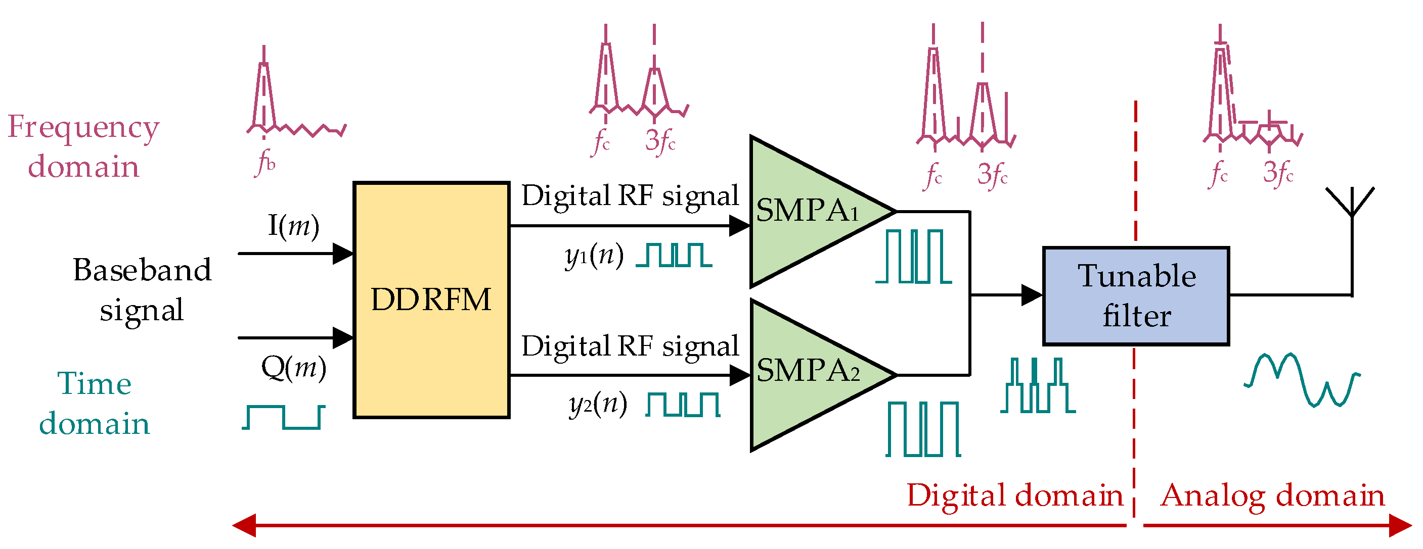
4]. It not only contains the features of a compact and logically programmable structure, but also meets the design requirements of low power consumption and high efficiency of the transmitter. To facilitate the physical implementation of the system, ADTx based on phase-shift control has been proposed [
5,
6], and its architecture is shown in
Figure 1. The direct digital radio frequency modulator (DDRFM) [
7] is used to complete the up-conversion and pulse encoding of the baseband signal. Subsequently, the two generated digital radio frequency (RF) pulse sequences are amplified by two switched-mode power amplifiers (SMPAs) [
8]. Finally, the signal is recovered by the tunable filter. Since the two-level pulse sequence can directly drive the rear amplifier, it does not need complicated signal processing. In order to achieve a three-level output, the baseband signal can be modulated in DDRFM first. Two two-level signals are obtained and then synthesized into a three-level one to reduce the difficulty of implementation. However, the two-level signal generation process inevitably contains a large amount of quantization noise. To ensure the spectral purity, certain pulse coding methods are needed to suppress the in-band and out-of-band noise [
9].
Delta-sigma modulation (DSM) [
10,
11,
12] and pulse-width modulation (PWM) [
13,
14,
15] are the most used pulse coding methods for DDRFM. DSM converts in-band quantization noise to out-of-band noise and has a high in-band signal-to-noise ratio. Nevertheless, it has lower coding efficiency (CE) and higher out-of-band suppression requirements for tunable filter. When it comes to PWM, radio frequency pulse width modulation (RF-PWM) [
16] has the advantages of simple structure and higher CE. Its noise is mainly reflected in the high-order harmonics, which can reduce the tunable filter design requirements. Given the advantages in terms of CE, spectral purity, and implementation complexity, RF-PWM is popular in ADTx applications.
PWM methods based on phase-shift control and mapping have gradually emerged in recent years. The phase-shift control method decomposes the carrier signal containing the modulation information into two phase-shift signals with the same amplitude. Then the two signals are synthesized after PWM separately to recover the original signal. It has the advantage of high linearity and high efficiency [
17]. In the case of the mapped pulse width modulation (MPWM) [
18,
19,
20]–based method, the mapping relationship between the input modulation information and the output pulse waveform is utilized. This method further improves the flexibility of DDRFM by implementing the direct output of PWM waveforms through mapping look-up tables. To reduce the implementation complexity, a DSM-MPWM method [
18] is presented. However, it may affect the optimal solution acquisition and cause low CE due to the use of a two-level output. Meanwhile, an intermedia frequency MPWM and its optimization scheme [
19,
20] are proposed for higher carrier flexibility and relaxed output filter requirements. As a result of unrestricted output pulse states, however, the system real-time performance is severely limited by the time resolution.
In this paper, a three-level RF-PWM method based on phase-shift control and MPWM is proposed for ADTx, which is used to improve the flexibility of ADTx and simplify the implementation structure. First, two look-up tables (LUTs) are created from the mapping relationship between the input amplitude phase and the pulse width position. Afterwards, these tables will be simplified by phase-shift-control-related characteristics. Next, the original signal is decomposed into two phase-shift signals for separate modulation. Moreover, a certain mapping strategy is explored to ensure the mapping accuracy and improve the modulation performance. Compared with existing MPWM techniques, the proposed method has significant advantages in terms of CE, system real time, and system complexity.
2. Architecture of Three-Level RF-PWM Scheme Based on Phase-Shift Control and MPWM
As shown in
Figure 2, the proposed system is a cascaded architecture of multiple modules, where the baseband sampling rate
fb is the carrier frequency
fc, the RF sampling rate
fRF is
N times of
fc, and
N is the length of the output pulse sequence in one pulse period
Tc. In the following, the whole modulation process and the roles of each module are described.
DSM module: Convert the digital baseband I(m) and Q(m) signals into DSM modulated signals with quantization level number lq. To obtain satisfactory in-band noise suppression, the DSM processing of I(m) and Q(m) is required before the CORDIC extracts amplitude-phase information. This module uses oversampling and noise shaping techniques to move the in-band noise out of band and then outputs the DSM modulated signals xi(m) and xq(m). In this case, the structure of the DSM is a second-order low pass.
CORDIC module: Convert xi(m) and xq(m) to amplitude and phase information ρ(m) and φ(m). At first, normalize the complex signal synthesized by xi(m) and xq(m), and then extract the amplitude-phase information (ρ(m), φ(m)) of the normalized complex signal.
Phase-shift control module: Convert ρ(m) and φ(m) into the two phase-shift signals φ1′(m) and φ2′(m). The two decomposed signals with the phases φ1′(m) and φ2′(m) and the amplitude of 1/2 can be obtained by derivation based on ρ(m) and φ(m).
MPWM module: Map φ1′(m) and φ2′(m) to the two two-level pulse sequences pk1(m) and pk2(m). Input φ1′(m) and φ2′(m) into the preset LUT for mapping lookup, respectively, and get the two two-level output pulse sequences pk1(m) and pk2(m).
Pulse generator: Convert pk1(m) and pk2(m) into the two-level RF pulse waveforms y1(n) and y2(n), respectively. The pulse sequences corresponding to all amplitude-phase information are sequentially spliced into the two-level pulse signals y1(n) and y2(n).
Adder: Synthesize the two-level y1(n) and y2(n) into the desired three-level RF-PWM signal y(n). Here, y(n) is used for simulation experiments to analyze the performance of the proposed scheme, and is not the real output of DDRFM.
3. Implementation of Phase-Shift Control and MPWM
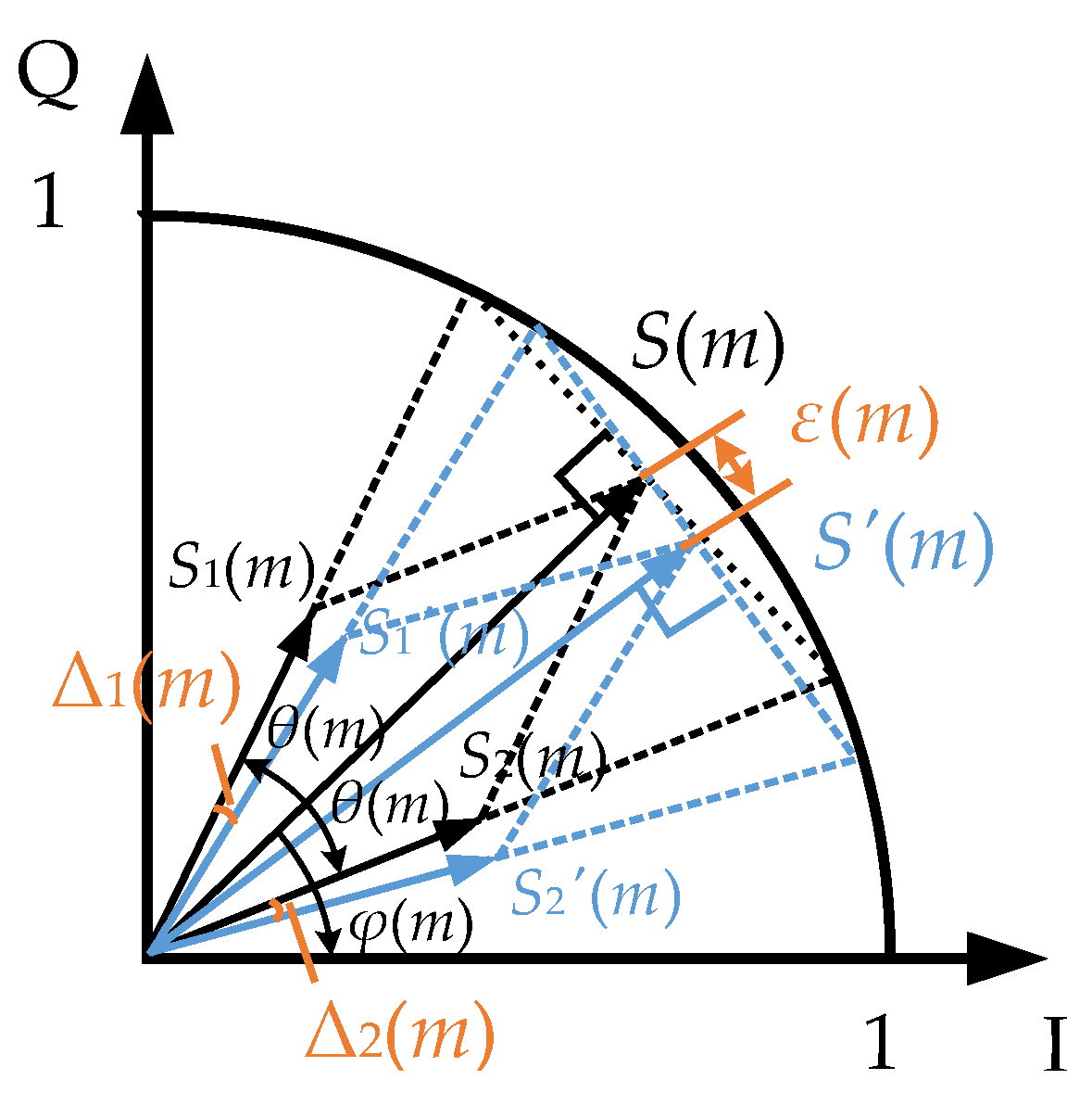
3.1. Error Analysis of Phase-Shift Control
The core of phase-shift control lies in signal decomposition, where the original signal containing amplitude-phase modulation information is decomposed into two-phase modulated signals with constant envelope. The vector decomposition of the original baseband modulated signal
S(
m) is shown in
Figure 3, given by
The original signal
S(
m) is decomposed into two phase-shift signals,
S1(
m) and
S2(
m). The amplitude of both signals is 1/2, and the phase is
φ(
m) +
θ(
m) and
φ(
m) −
θ(
m), respectively. Here,
θ(
m) is the phase-shift angle [
17], calculated by
In this scheme, the phase-shift signals need to be converted to pulse sequences by MPWM before synthesizing the original signal. The phase errors introduced by the mapping in this process are set to Δ
1(
m) and Δ
2(
m). After mapping, the actual decomposed signals used for signal recovery are
S1′(
m) and
S2′(
m), which can be written as
and
At this point, the phases
φ1′(
m) and
φ2′(
m) of
S1′(
m) and
S2′(
m) have
φ1′(
m) =
φ(
m) +
θ(
m) − Δ
1(
m) and
φ2′(
m) =
φ(
m) −
θ(
m) − Δ
2(
m), respectively. The vector synthesis signal of
S1′(
m) and
S2′(
m) is
S′(
m). Consequently, the error between
S′(
m) and the original signal can be represented as
As can be seen from Formula (5), to eliminate the error between the synthesized signal and the original signal as much as possible, Δ1(m) and Δ2(m) should be close to 0. Accordingly, increasing the phase resolution among MPWM is the key to improve the mapping accuracy in this scheme.
3.2. Creation of LUTs for MPWM Module
The core of the MPWM technique lies in the establishment of LUTs. First of all, two LUTs can be created, which are the phase mapping table Q and the two-level pulse mapping table P. The one-to-one mapping of them is realized by the correspondence between the amplitude-phase information of the input modulated signal and the pulse width position of the pulse sequence.
Let there be K possible cases of output pulse sequences, and P is the combination of all two-level output pulse sequences. That is, P = [p1, ..., pi, ..., pK] and pi = [p1, ..., pj, ..., pN]; i and j are any integers not more than K and N, respectively; and pj is 1 or 0. In this proposed scheme, the amplitude of both phase-shift signals is 1/2, which means that the input amplitude of the MPWM module is fixed at 1/2. Considering that the amplitude of the input signal is related to the pulse width of the pulse sequence, the pulse sequence corresponding to the phase-shift signal must have the same pulse width. In this work, the two-level pulse sequence with a duty cycle of 50% is selected for synthesizing the required three-level RF-PWM signal. To decrease the switching frequency of pi, it is required that “1” appears in a continuous position, which indicates that Tc has only one continuous positive pulse. Thus, the pulse width of any pulse sequence pi is N/2, while there are N possible pulse positions. It is obvious that pi has a total of K = N possible cases.
Q is the combination of amplitude-phase information (
ρp_i,
φp_i) corresponding to all
pi, where
Q = [
q1, ...,
qi, ...,
qK].
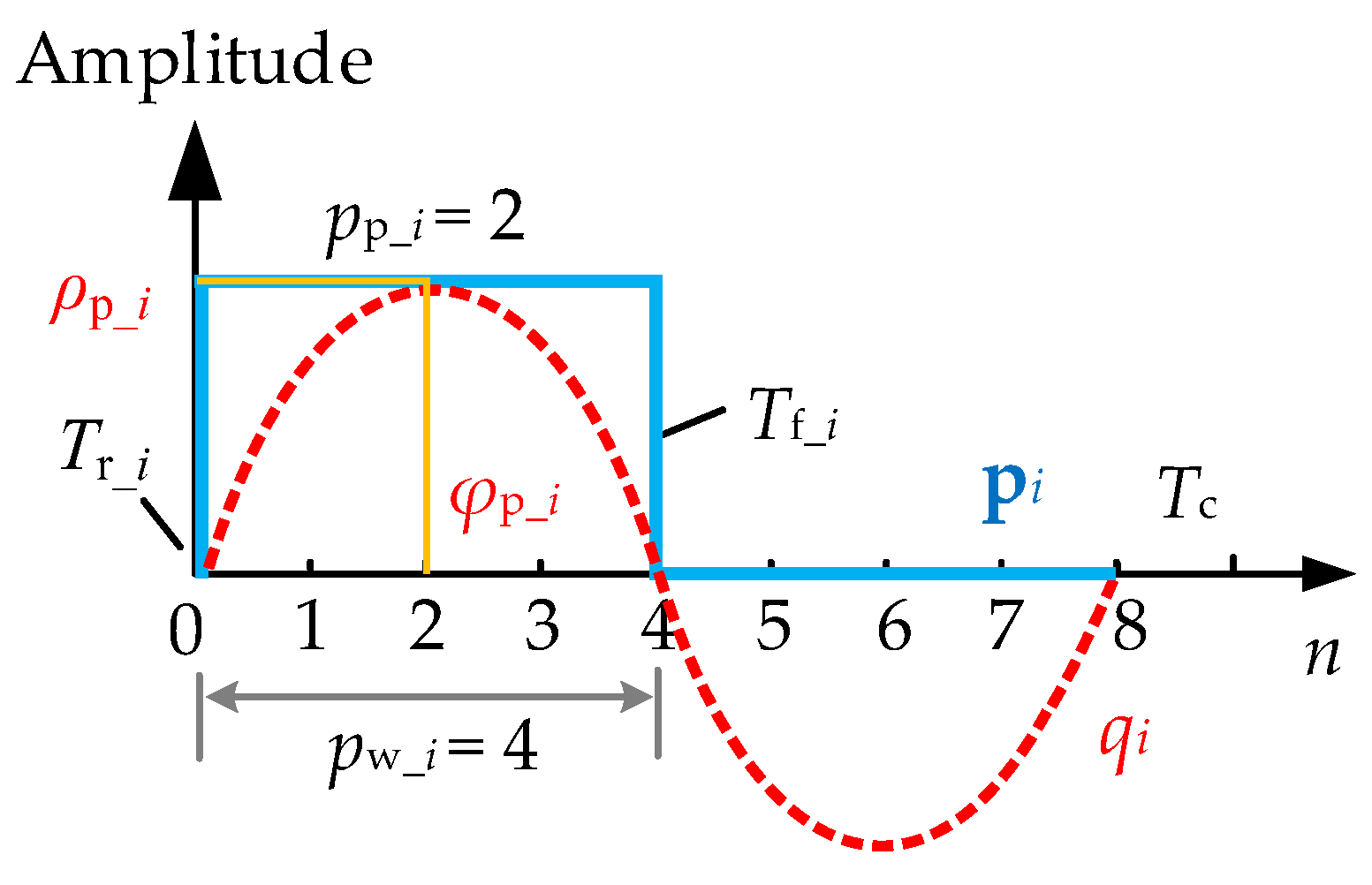
Figure 4 shows the mapping relationship between the pulse sequence
pi and its fundamental signal
qi. Here,
pi is a special case of the actual decomposed signal
S1′(
m) or
S2′(
m) with a pulse width of 4 and a pulse position of 2. Furthermore, according to the characteristics of the decomposed signal shown in
Figure 3, the
pi in
Figure 4 is constrained to a state where the half cycle is on and the amount of phase shift determines the pulse position. Since the amplitude of its fundamental signal is related to the pulse width, then the amplitude
ρp_i will be limited to be constant and only related to the modulator gain
A. Let
Tr and
Tf be the rising and falling edges of the pulse, respectively; then the pulse width
pw =
Tf −
Tr =
N/2 and the pulse position
pp = (
Tf +
Tr)/2. In
Figure 4,
N = 8,
pw_i = 4, and
pp_i = 2. The mapping relationship between
qi and
pi [
20] can be expressed as
4. Mapping Lookup Strategy in MPWM
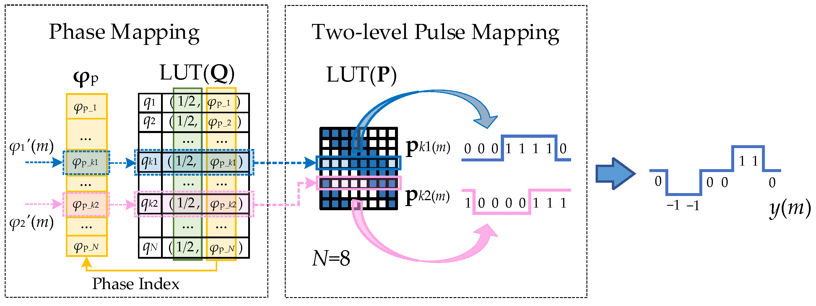
In order to ensure the system real time while keeping the mapping error as small as possible, a specific mapping lookup strategy is required to look up the table for Q. After that, the corresponding pulse sequence is obtained by looking up in P according to the aforementioned one-to-one mapping relationship between P and Q. This MPWM process is divided into two main steps, phase mapping and two-level pulse mapping.
According to Formula (6), it is known that Q is distributed in a circular shape in the complex plane. For the convenience of analysis, polar coordinates are used for mapping analysis. Let (1/2, φ(m)) be the mapping input and (1/2, φp_i) be the mapping output qi. Usually, the MPWM with unrestricted pulse states needs to calculate the vector error for both one by one. Then, qi with the smallest vector error is taken as the optimal mapping qk, where k is an integer not larger than N. This traversal lookup method requires N times of error calculation and N-1 times of comparison. It ensures that the mapping error of the search result is minimized, but inevitably causes redundant computations.
To facilitate mapping lookups, set
A = 1/2, which means that all
ρp_i in
Q are 1/2. By using the concept of phase-shifting control to limit the pulse states, it is possible to determine
qk by simply finding the nearest value of the input phase. Its optimal mapping can be achieved without even any error calculation and comparison. The amplitude-phase information of the two phase-shift signals is (1/2,
φ1′(
m)) and (1/2,
φ2′(
m)). As shown in
Figure 5, based on the established
P and
Q, the specific mapping steps for MPWM are as follows:
Create a phase index table φp. The elements in φp are direct extracts of the phase information in Q with length N.
Determine the optimal mapping qk1 and qk2 by phase mapping on φp. Taking φ1′(m) and φ2′(m) as inputs, suppose φp_k1 and φp_k2 are the nearest phases of the two inputs, respectively. Then (1/2, φp_k1) and (1/2, φp_k2) in Q are the desired qk1 and qk2.
Determine the two-level pulse sequences pk1(m) and pk2(m) by two-level pulse mapping. According to the one-to-one correspondence between P and Q, pk1(m) and pk2(m) corresponding to qk1 and qk2 can be found in P. Moreover, the maximum amplitude of its vector synthesis y(m) is 1.
To obtain the desired mapping accuracy and increase the phase resolution of the MPWM, this paper considers increasing the phase resolution of both the input and output signals of the MPWM module. For DSM modules, quantification is an irreversible process. It converts an infinite number of input amplitude values into a finite number of output amplitude values. The quantization noise of the quantizer decreases exponentially as the number of quantization levels
lq increases, thus providing a significant effect on the CE [
10]. As can be seen,
N is related to the time resolution and directly affects the mapping accuracy. Based on the above, this paper will explore its impact on the MPWM module for
N and
lq.
Figure 6 shows the distribution of the mapping input signal and the mapping output signal
qi in the first quadrant of the mapping space for different
N and
lq conditions, where the round dots are the mapping input signals and the diamond dots are the mapping output signals represented by
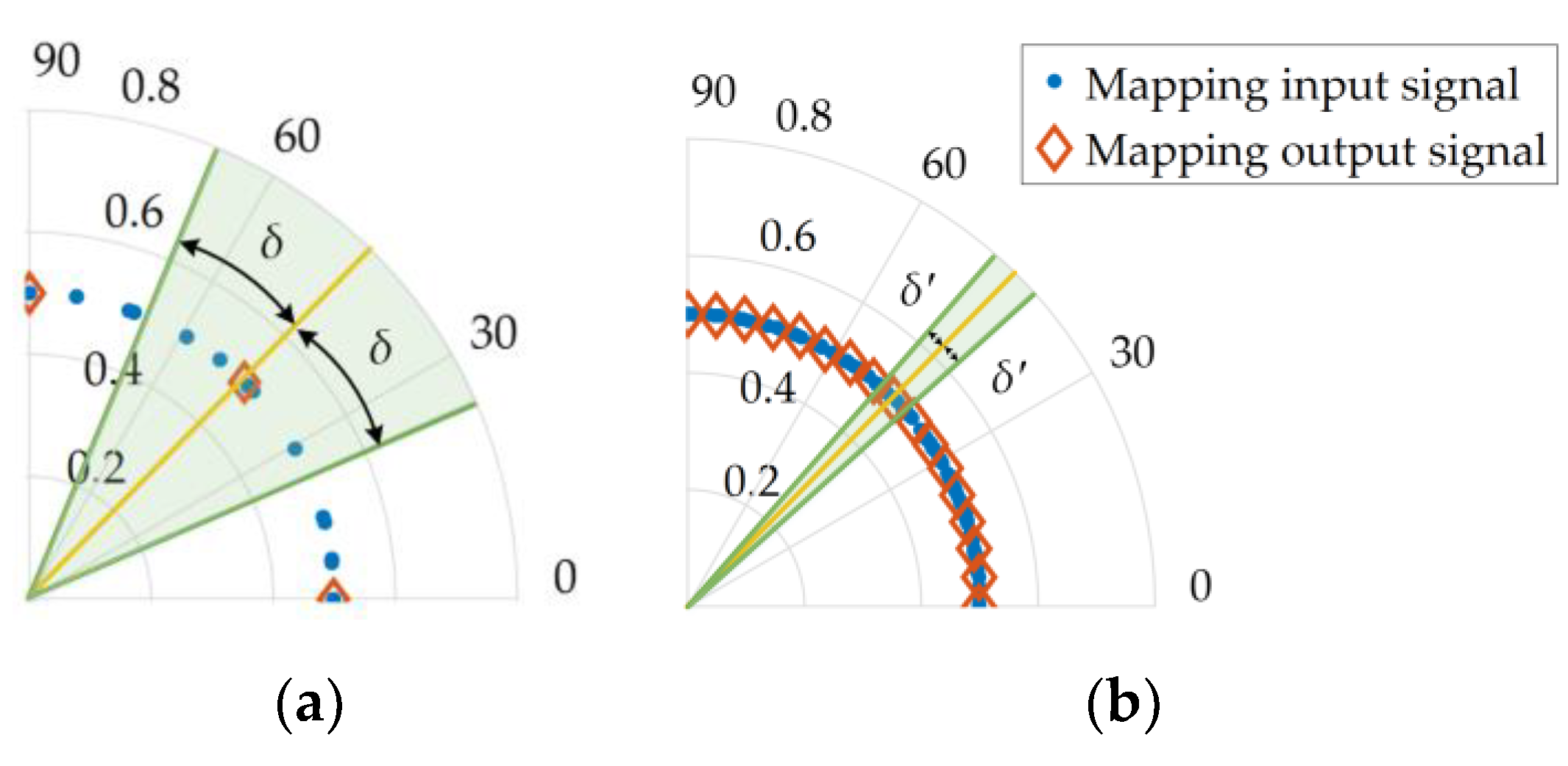
qi. In
Figure 6a, there have
N = 8,
lq = 8, and the mapping input points within the green shading have the same mapping output points. In this case, the green shading is the area ±
δ around the mapping output point. According to the table-building property of
Q, it is known that the phase difference between adjacent
qi is 2π/
N. Therefore,
δ = π/
N. It follows that to reduce the mapping error,
δ should be as small as possible, which means that
N should be as large as possible. In
Figure 6b,
N = 64,
lq = 30. It can be seen that as
N and
lq increase, the phase resolution of the mapping input and output signals is increased. At the same time, to achieve the desired mapping accuracy, the mapping input and output signals need to maintain a certain degree of fitness. In summary, the larger the values of
N and
lq, the better the modulation performance improvement. Moreover, it is easy to see that increasing the phase resolution of the MPWM module has a relatively higher demand on
N. This further reflects the need to ensure the real-time performance of the system.
Besides considering the conventional performance indicators, such as CE, adjacent channel power ratio (ACPR), and error vector magnitude (EVM) of the modulation scheme, it is crucial to investigate the mapping noise generated in the MPWM process. It reflects the signal purity and can be calculated by
5. Simulation and Experimentation
To verify the modulation scheme and mapping strategy proposed in this paper, simulations and offline experiments were implemented. A 16QAM modulated signal with
fc = 300 MHz and different bandwidth BWs of 5 and 10 MHz was used as input. SI is a three-level RF-PWM scheme based on phase-shift control with a fixed threshold comparison [
17], and SII is the proposed scheme. In this paper, the parameters related to the phase resolution of the proposed scheme were first investigated on MATLAB. Then the two pulse coding schemes were simulated and tested. What is more, an actual test comparison was realized using the arbitrary waveform generator AWG7122C.
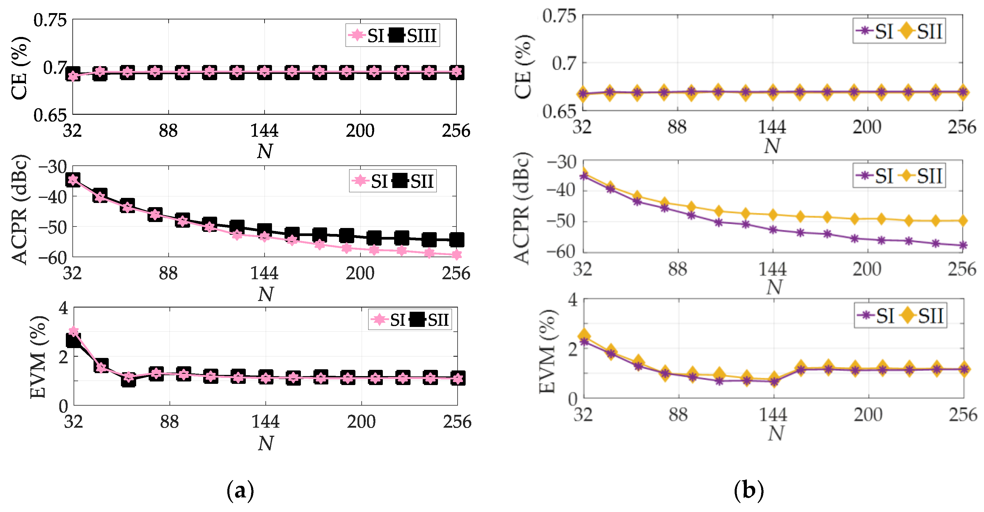
5.1. Simulation
Figure 7 shows the trend of the output performance indicators of SII for different BWs of the input signal. In this case,
N = 64 when investigating the effect of
lq on the main modulation performance, and
lq = 128 when investigating
N. As shown in the figure, the improvement effect of
lq on CE is limited, while CE is insensitive to
N. Nevertheless, the increase in these two parameters has a significant effect on the optimization of ACPR, EVM, and
Pε. After a certain range (about
lq > 64,
N > 96), the change of the related linearity indicators shows a slow decreasing trend. For input signals with different BWs, the narrower the BW, the better the relative performance. Meanwhile, BW does not affect the mapping error. In summary,
lq and
N are indeed important parameters that affect the modulation performance of this scheme.
In addition, the output spectrum and adjacent channel spectrum of SI and SII with different modulation parameters are given in
Figure 8. Here, BW = 5 MHz; the generation of even harmonics mainly derives from the truncation error caused by quantization. As can be seen from the above analysis, the output modulation performance indicators were basically unchanged when
N = 64 and
lq > 128 for SII. However, it can be seen from
Figure 8 that the out-of-band noise can still be effectively suppressed by continuously increasing
lq. It is calculated that when SII is taken as
lq = 512, the noise floor is reduced by nearly 5 dB compared with
lq = 128. At the same time, by increasing
lq, the SII out-of-band noise and harmonic suppression effect can basically reach the performance level of SI. This can simplify the output filter design to some extent. Apart from the obvious out-of-band suppression effect of
lq, increasing the value of
N is also the most direct and effective way to reduce in-band and out-of-band noise. When
N = 256, not only the noise floor is reduced, but also the clear bandwidth of SII will be broadened. The adjacent channel noise ratio is reduced by about 11 dB compared with
N = 64.
Accordingly, to find the better modulation performance of SII on the basis of the above, the main performance comparison with SI at
lq = 512 is given in
Figure 9. It can be seen that the two schemes have nearly identical modulation performance and variation trends in terms of CE and EVM. For ACPR, the performance results are closer for a narrower BW. This shows that the proposed scheme, with a completely different modulation, can achieve a performance level comparable to SI to a certain extent. It also validates the effectiveness and reliability of this scheme. Under simulated conditions, the best modulation performance indicators for the SII can be achieved: CE of approximately 70%, ACPR < −50 dBc, and EVM < 1%.
5.2. Off-Line Experiments
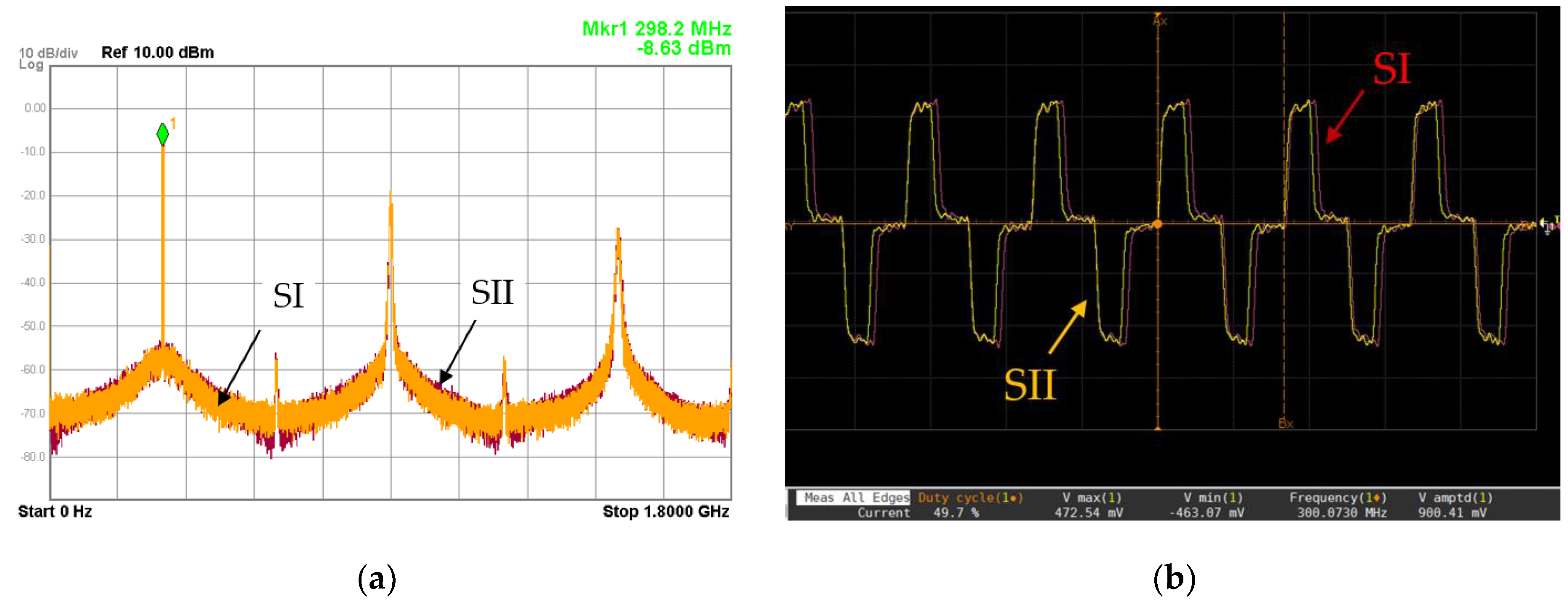
As shown in
Figure 10, this paper uses an off-line experimental approach [
21] to compare and validate the measured spectrum and time domain waveforms of the SI and SII. First, the output pulse sequences for both schemes are calculated and saved on the PC. Then, they are downloaded into the AWG7122C (
fs up to 24 Gsps) to generate the corresponding three-level RF-PWM signals. Finally, the signals are input to a digital scope and a vector signal analyzer (VSA) for testing. Set
fc = 300 MHz,
N = 64, and sampling frequency
fRF = 19.2 Gsps.
A comparison of the measured spectrum and time domain waveforms of the two schemes is given in
Figure 11. It can be seen that the SII can effectively suppress the in-band and out-of-band noise through phase shifting and mapping modulation. The measured output spectrum and time domain waveforms are nearly identical to those of the SI, and are in general agreement with the simulated waveforms. This once again demonstrates the feasibility and effectiveness of the proposed strategy.
Table 1 gives a comparison of the main modulation performance indicators for the two schemes and the related references. Compared with the references [
18,
20], the proposed scheme in this paper improves the CE by more than 20%. However, there is a gap in the ACPR of the SII at
N = 64 (still achieves −45 dBc), which is mainly due to the constraints on the waveform of the output pulse by the SII. The constrained pulse state may affect the optimal solution acquisition for mapping lookup, resulting in a relatively high requirement for time resolution in SII. Nevertheless, comparing the LUT sizes for the same variables, the proposed scheme greatly simplifies the LUT. It demonstrates that the proposed scheme is effective in relaxing the restrictions on
N while ensuring real-time performance of the mapping system. The time resolution in [
20] can only be taken to 6.25% (
N = 16). In contrast, the time resolution of the proposed scheme in this paper can be taken to 0.39% or even lower (
N can be larger than 256). For the SI, the SII at
N = 64 has the same conclusion as the simulation: the SII achieves modulation performance comparable to the SI.
6. Conclusions
In this paper, a three-level RF-PWM method based on phase-shift control and MPWM (SII) is first proposed. This approach allows the two two-level outputs to drive the rear PA directly, greatly simplifying the system implementation structure. Then, to ensure the desired mapping accuracy and modulation performance, this paper also improves the phase resolution of the mapping correlation signal for error analysis. Finally, the feasibility and effectiveness of the SII is verified by simulation and offline experiments. The results show that this scheme can effectively improve the overall performance of the system through mapping modulation and parameter adjustment. Its best modulation performance indicators can be achieved: CE at about 70%, ACPR < −50 dBc, EVM < 1%. Comparing the SII with existing three-level RF-PWM schemes based on phase-shift control (SI), the SII can achieve a performance level comparable to the SI in terms of key indicators and out-of-band spectral characteristics under the same conditions. Compared with the existing MPWM technology, this scheme has significant advantages in both CE and real-time performance. There is at least a 20% improvement in CE compared with [
18], with an effective improvement in the real-time performance of the system at the same
N. Compared with [
20], the CE is improved by more than 55%, and the time resolution can be taken from 6.25% to 0.39%.
In addition, an FPGA-based platform is being built to implement the scheme proposed in this paper. The next step in the work will be the experimental verification of the specific implementation circuit. The proposed scheme in this paper can effectively simplify the physical implementation structure and solve the problem that the system’s real-time performance is limited by the time resolution. In view of the various requirements in practical applications, the algorithm for completing multiobjective optimization while implementing the above scheme is being further debugged.
Author Contributions
Conceptualization, S.Z. and Q.Z.; methodology, S.Z. and Q.Z.; software, S.Z. and L.Z.; validation, S.Z. and L.Z.; formal analysis, S.Z., L.Z., J.Z. and H.F.; investigation, S.Z., L.Z., J.Z. and H.F.; resources, Q.Z.; data curation, S.Z.; writing—original draft preparation, S.Z.; writing—review and editing, S.Z. and Q.Z.; visualization, S.Z.; supervision, Q.Z. and S.Y.; project administration, Q.Z. and S.Y.; funding acquisition, Q.Z. All authors have read and agreed to the published version of the manuscript.
Funding
This research was funded by the National Natural Science Foundation of China (61631021).
Conflicts of Interest
The authors declare no conflict of interest.
References
- Kuo, N.-C.; Yang, B.; Wang, A.; Kong, L.; Wu, C.; Srini, V.P.; Alon, E.; Nikolić, B.; Niknejad, A.M. A 0.4-to-4-GHz all-digital RF transmitter package with a band-selecting interposer combining three wideband CMOS transmitters. IEEE Trans. Microw. Theory Tech. 2018, 66, 4967–4984. [Google Scholar]
- Zhu, L.; Zhou, Q.; Wei, Z.H.; Chen, J.B. A novel all digital transmitter with three-level quadrature differential RF-PWM. In Proceedings of the Journal of Physics: Conference series, Orlando, FL, USA, 10–14 October 2021. [Google Scholar]
- Mitola, J. The software radio architecture. IEEE Commu. Mag. 1995, 33, 26–38. [Google Scholar] [CrossRef]
- Kirillov, S.N.; Lisnichuk, A. Adaptive to interference software-defined transmitter and receiver of radio signals based on multi-criteria synthesis of signal set. In Proceedings of the 2020 International Scientific and Technical Conference Modern Computer Network Technologies (MoNeTeC), Moscow, Russia, 27–29 October 2020. [Google Scholar]
- Cho, K.; Gharpurey, R. A 25.6 dBm wireless transmitter using RF-PWM with carrier switching in 130-nm CMOS. In Proceedings of the 2015 IEEE Radio Frequency Integrated Circuits Symposium (RFIC), Phoenix, AZ, USA, 17–19 May 2015. [Google Scholar]
- Cho, K.; Gharpurey, R. A digitally intensive transmitter/PA using RF-PWM with carrier switching in 130 nm CMOS. IEEE J. Solid-State Circuits 2016, 51, 1188–1199. [Google Scholar] [CrossRef]
- Shen, Y.; Bootsman, R.; Alavi, M.S.; Vreede, L.C.N. A 1–3 GHz I/Q interleaved direct-digital RF modulator as a driver for a common-gate PA in 40 nm CMOS. In Proceedings of the 2020 IEEE Radio Frequency Integrated Circuits Symposium (RFIC), Los Angeles, CA, USA, 4–6 August 2020. [Google Scholar]
- Shiwarkar, N.V.; Bhat, A.P.; Rewatkar, K.G. Linear power amplifiers: Basic considerations of switched-mode assisted amplifiers. Int. J. Mod. Trends Eng. Res. 2015, 2, 79–85. [Google Scholar]
- Kumar, N.; Rawat, K.; Ghannouchi, F.M. Reconfigurable digital delta-sigma modulation transmitter architecture for concurrent multi-band transmission. IEEE Trans. Circuits Syst. I Reg. Pap. 2020, 67, 2455–2466. [Google Scholar] [CrossRef]
- Feng, D.; Bonizzoni, E.; Maloberti, F.; Sin, S.; Martins, R.P. A 10-MHz bandwidth two-path third-order SigmaDelta modulator with cross-coupling branches. IEEE Trans. Circuits Syst. II Exp. Briefs 2018, 65, 1410–1414. [Google Scholar] [CrossRef]
- Kumar, N.; Rawat, K. Delta-sigma modulation based digital transmitter for single and dual band transmission. In Proceedings of the 2018 IEEE MTT-S International Microwave and RF Conference (IMaRC), Kolkata, India, 28–30 November 2018. [Google Scholar]
- Chung, S.; Ma, R.; Shinjo, S.; Yamanaka, K.; Teo, K.H. A concurrent triple-band digital transmitter using feedforward noise cancellation for delta-sigma modulation. In Proceedings of the 47th European Microwave Conference (EuMC), Nuremberg, Germany, 10–12 October 2017. [Google Scholar]
- Nuyts, P.A.J.; Singerl, P.; Dielacher, F.; Reynaert, P.; Dehaene, W. A fully digital delay line based GHz range multimode transmitter frontend in 65-nm CMOS. IEEE J. Solid-State Circuits 2012, 47, 1681–1692. [Google Scholar] [CrossRef]
- Nuyts, P.A.J.; Reynaert, P.; Dehaene, W. A fully digital PWM-based 1 to 3 GHz multistandard transmitter in 40-nm CMOS. In Proceedings of the 2013 IEEE Radio Frequency Integrated Circuits Symposium (RFIC), Seattle, WA, USA, 2–4 June 2013. [Google Scholar]
- Hezar, R.; Ding, L.; Banerjee, A.; Hur, J.; Haroun, B. A PWM based fully integrated digital transmitter/PA for WLAN and LTE applications. IEEE J. Solid-State Circuits 2015, 50, 1117–1125. [Google Scholar] [CrossRef]
- Raab, F. Radio frequency pulsewidth modulation. IEEE Trans. Commu. 1973, 21, 958–966. [Google Scholar] [CrossRef]
- Chung, S.; Ma, R.; Shinjo, S.; Nakamizo, H.; Parsons, K.; Teo, K.H. Concurrent multiband digital outphasing transmitter architecture using multidimensional power coding. IEEE Trans. Microw. Theory Tech. 2015, 63, 598–613. [Google Scholar] [CrossRef]
- Markert, D.; Yu, X.; Heimpel, H.; Fischer, G. An all-digital, single-bit RF transmitter for massive MIMO. IEEE Trans. Circuits Syst. I Reg. Pap. 2017, 64, 696–704. [Google Scholar] [CrossRef]
- Yang, J.; Yang, S.Y.; Chen, Z.H.; Zhang, X.Y. An agile LUT-based all-digital transmitter. IEEE Trans. Circuits Syst I, Reg. Pap. 2020, 67, 5550–5560. [Google Scholar] [CrossRef]
- Yang, S.Y.; Yang, J.; Zhao, J.; Zhang, X.Y. Clean bandwidth improvement of MPWM encoding method for RF all-digital transmitter. IEEE Trans. Circuits Syst. II Exp. Briefs 2021, 68, 2404–2408. [Google Scholar] [CrossRef]
- Yao, F.Q.; Zhou, Q.; Zhu, L. A novel multilevel RF-PWM method with active-harmonic elimination for all-digital transmitters. IEEE Trans. Microw. Theory Tech. 2018, 66, 3360–3373. [Google Scholar] [CrossRef]
| Publisher’s Note: MDPI stays neutral with regard to jurisdictional claims in published maps and institutional affiliations. |
© 2022 by the authors. Licensee MDPI, Basel, Switzerland. This article is an open access article distributed under the terms and conditions of the Creative Commons Attribution (CC BY) license (https://creativecommons.org/licenses/by/4.0/).


