
A 3.95 ppm/°C 7.5 μW Second-Order Curvature Compensated Bandgap Reference in 0.11 μm CMOS


Abstract
:1. Introduction
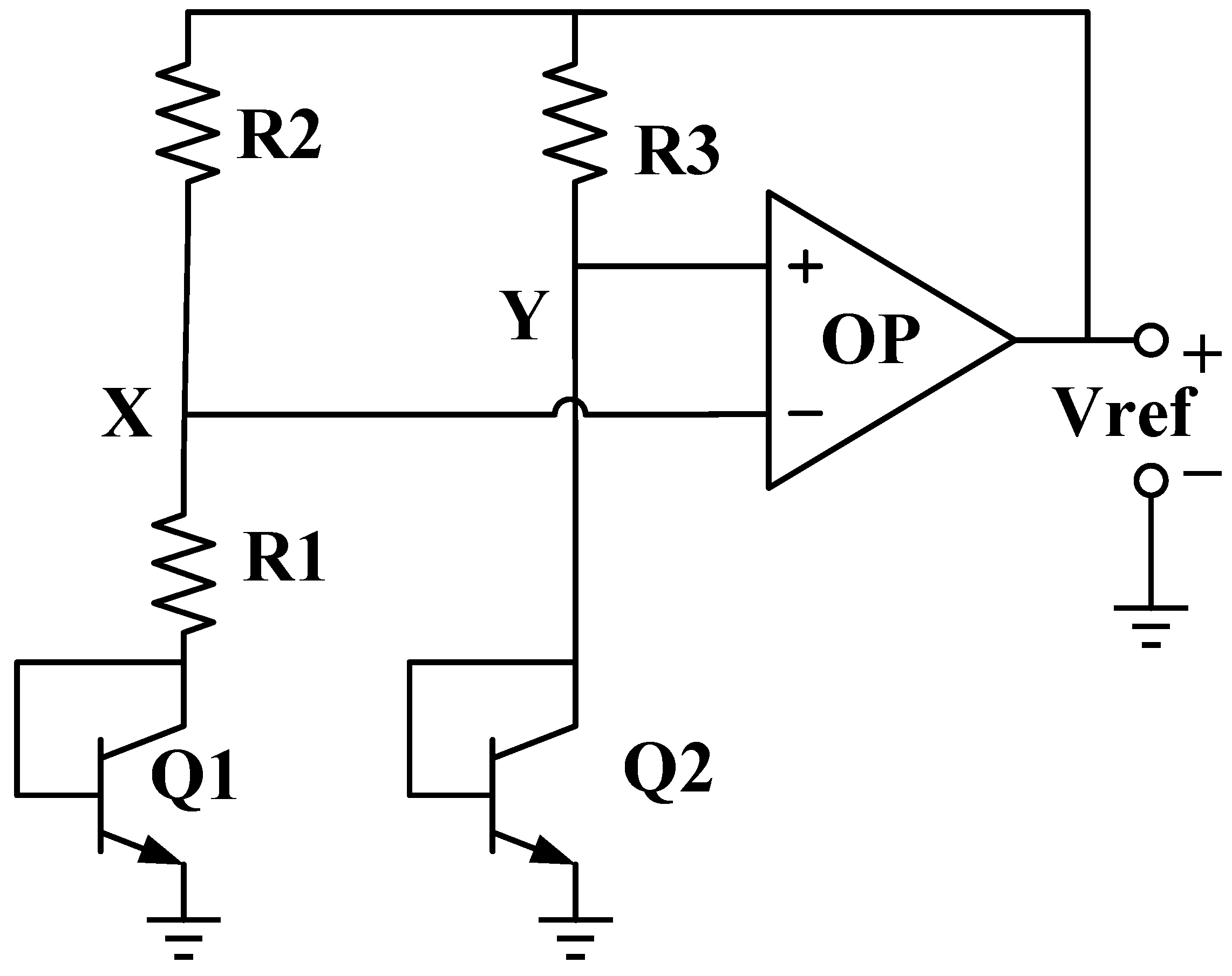
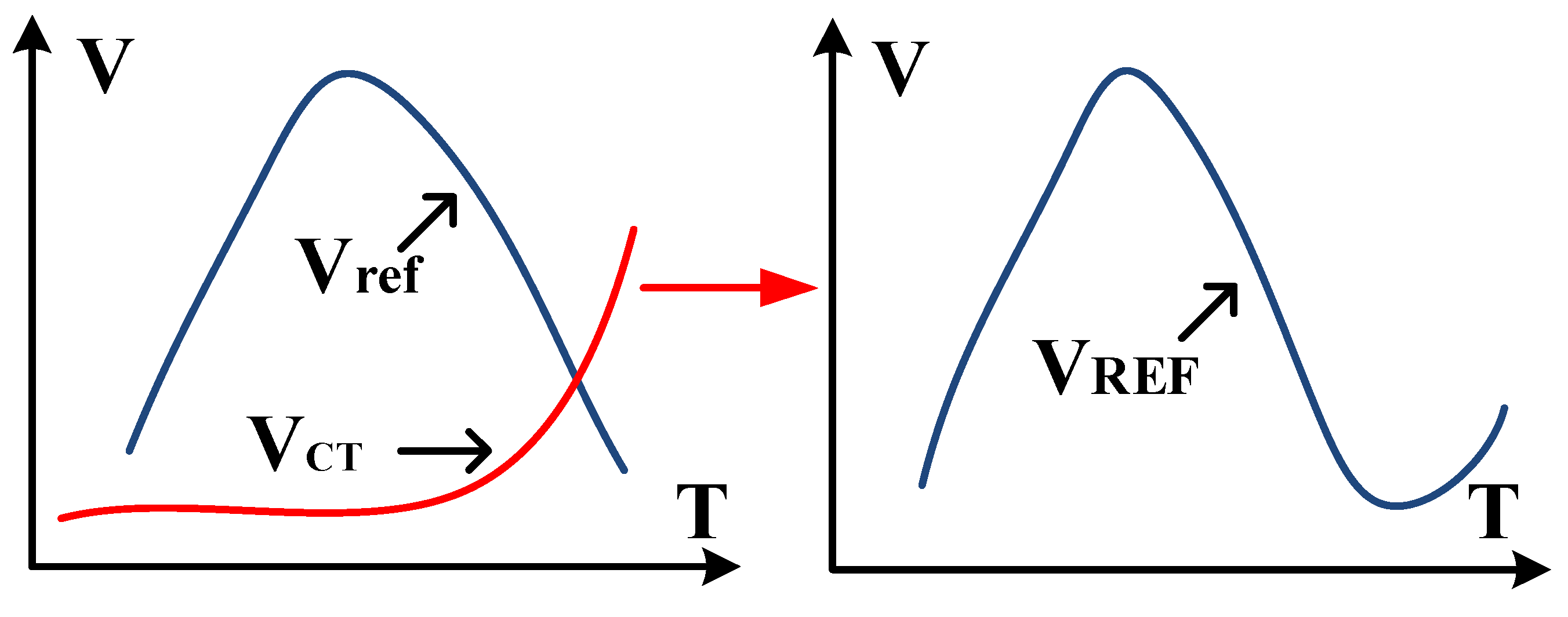
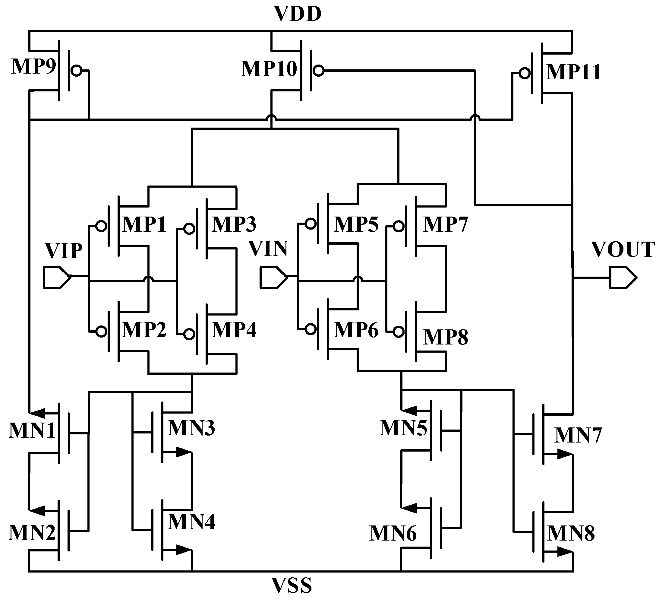
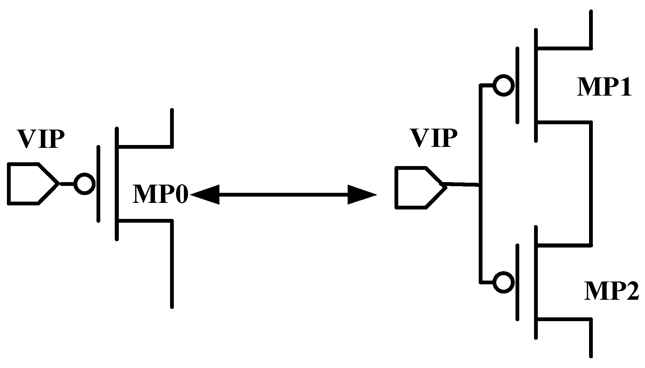
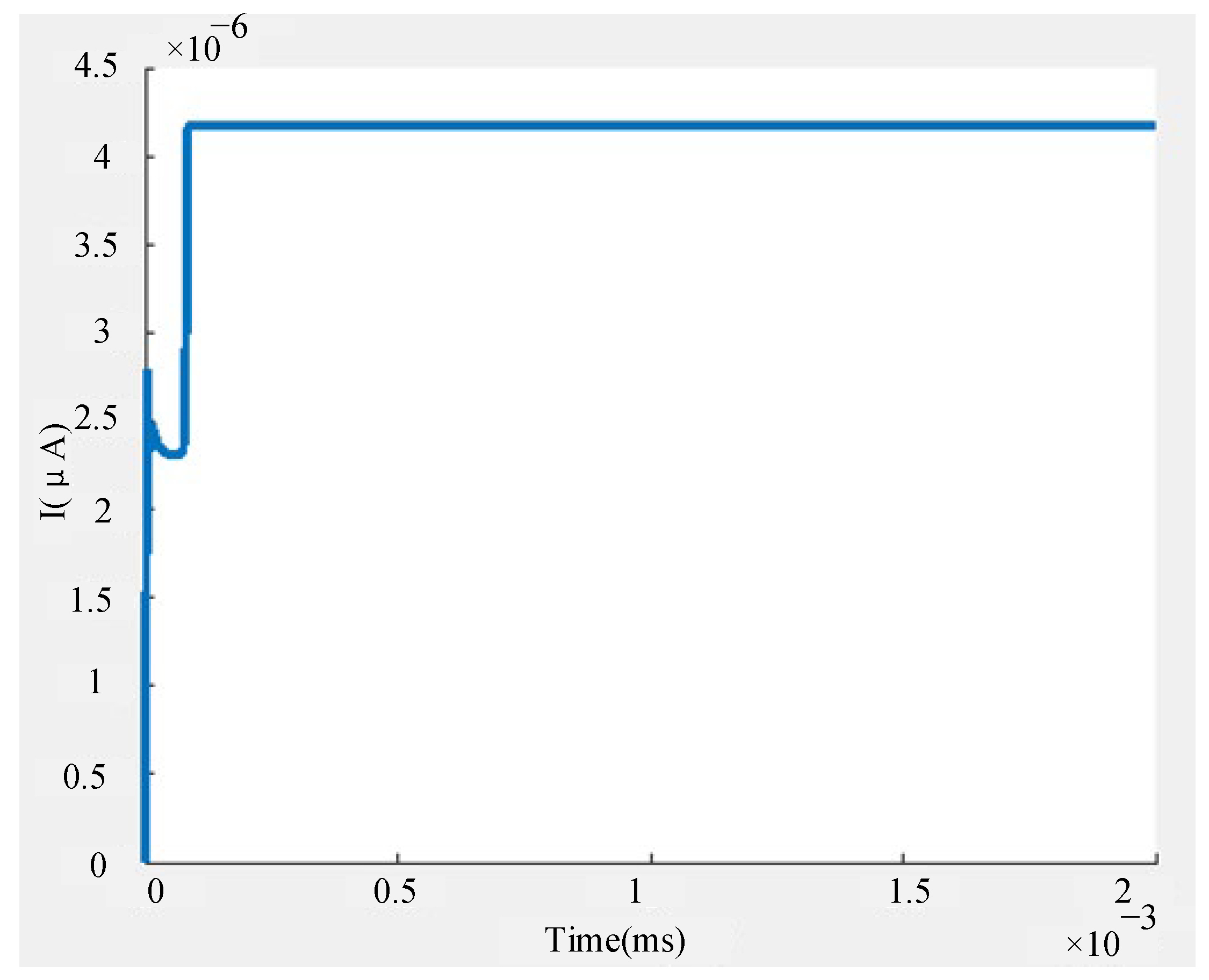
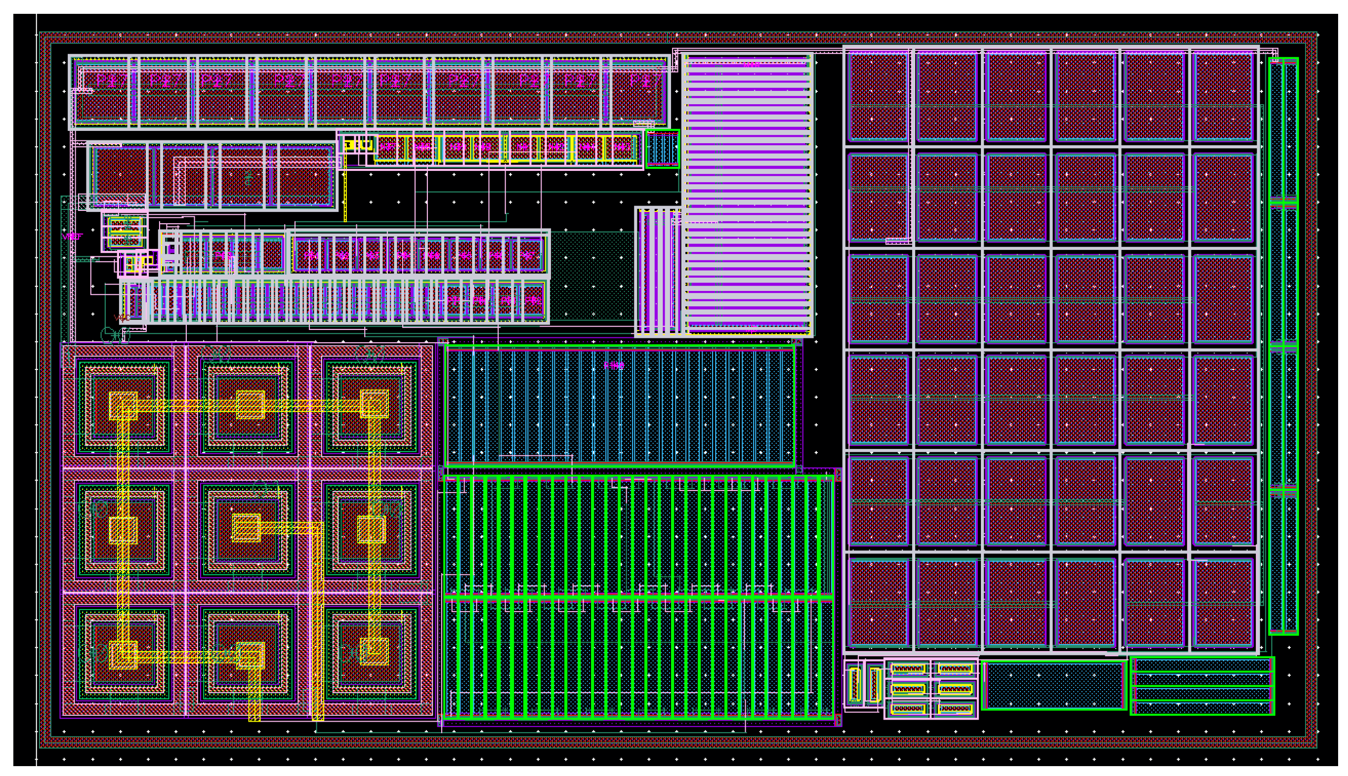
2. Proposed Design
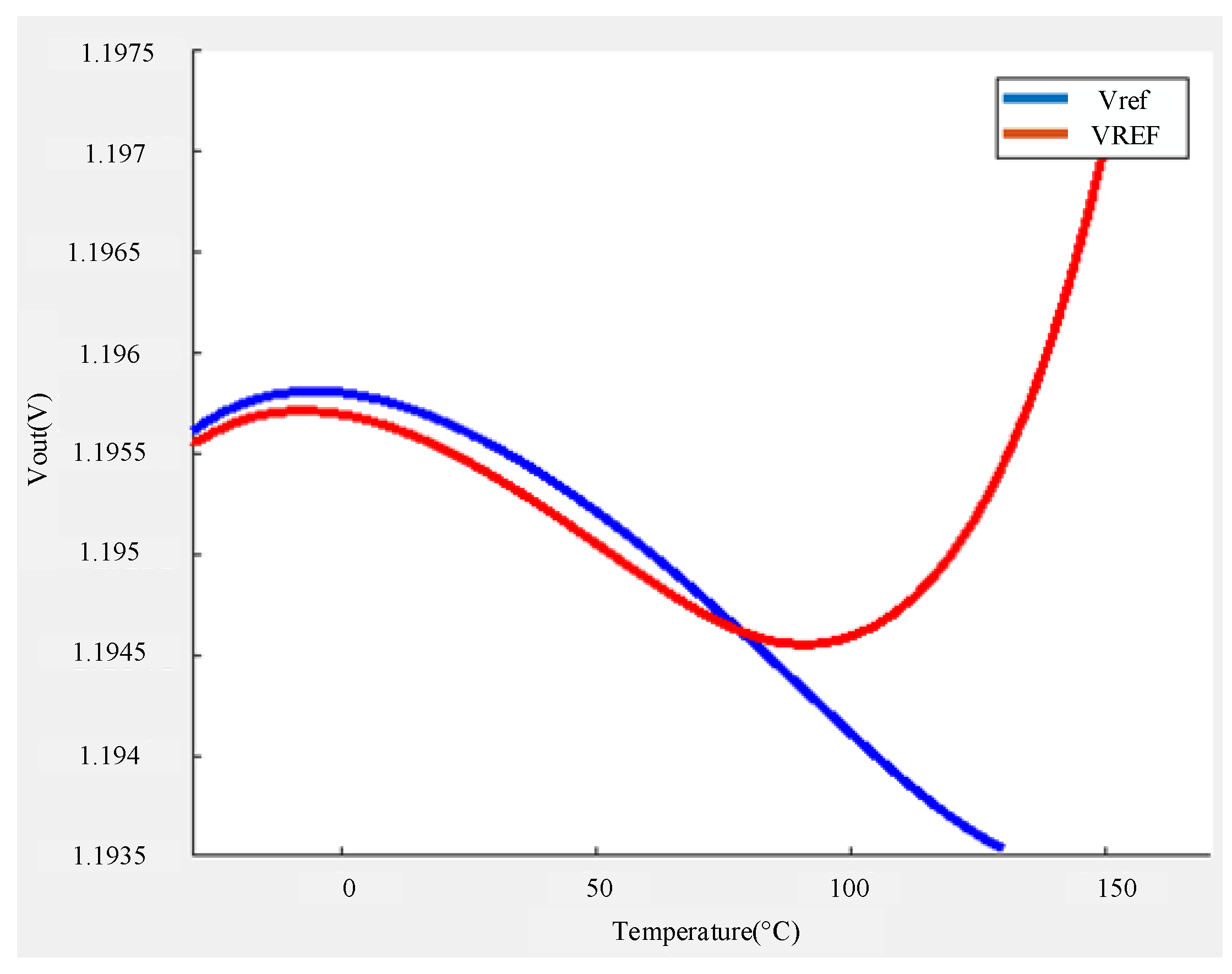
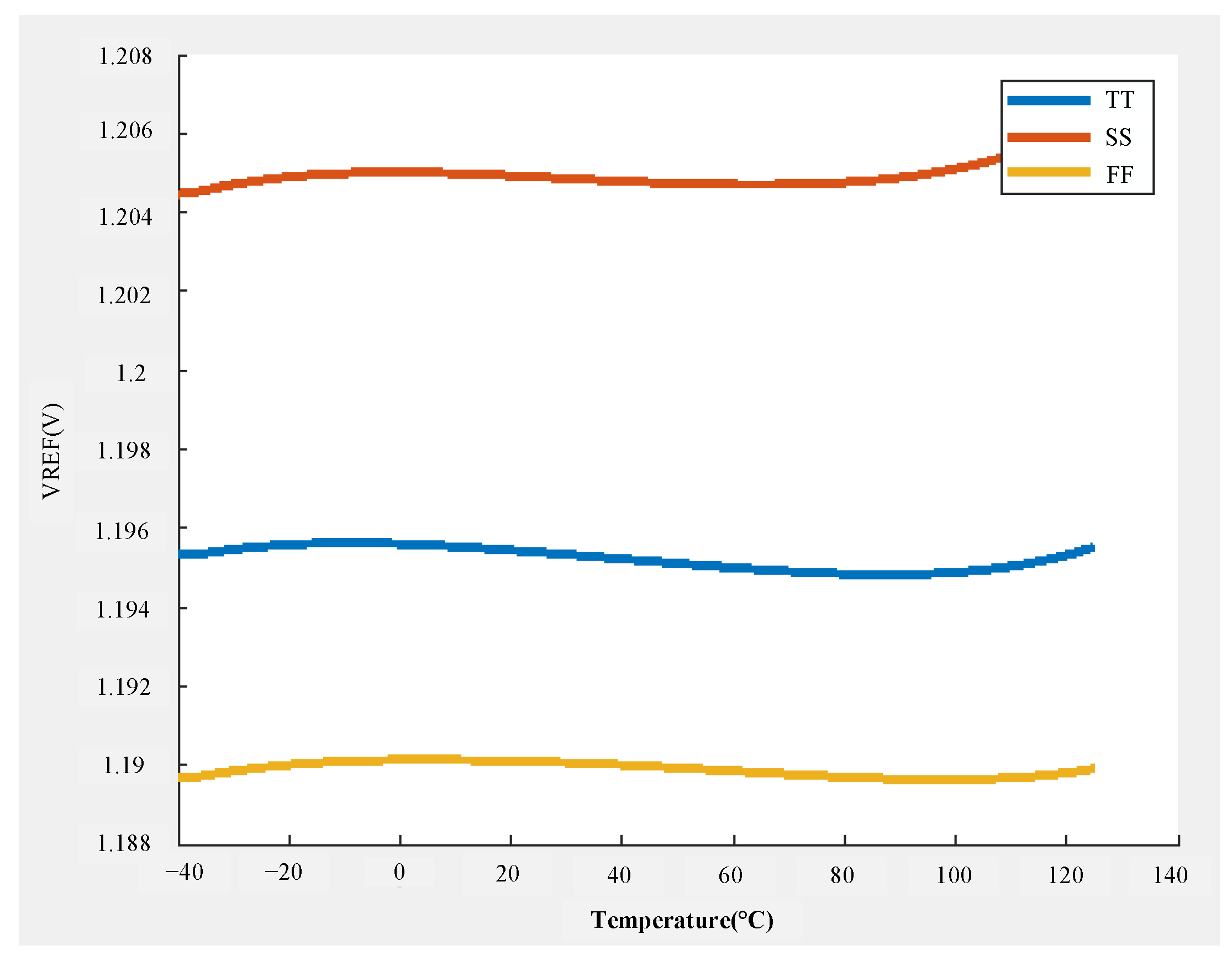
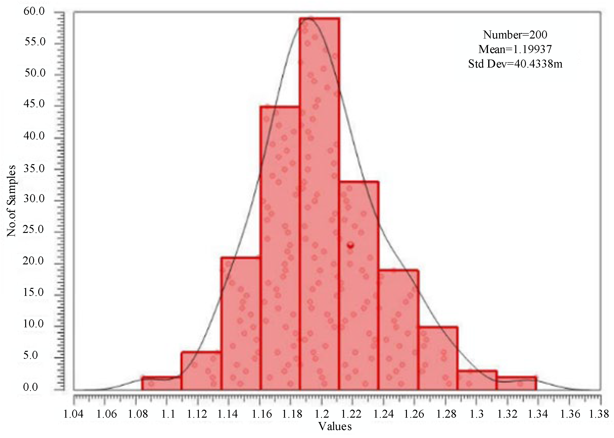
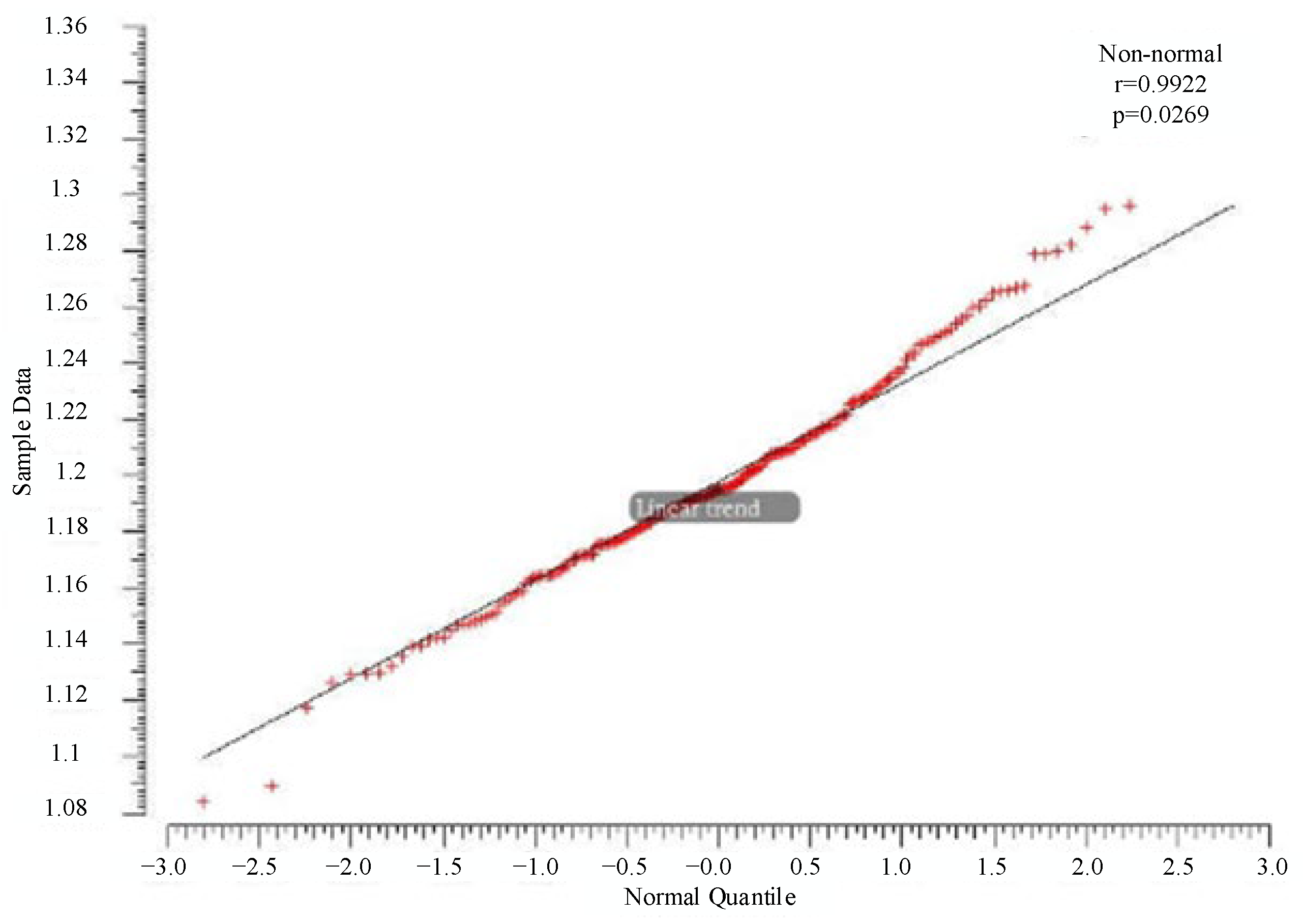
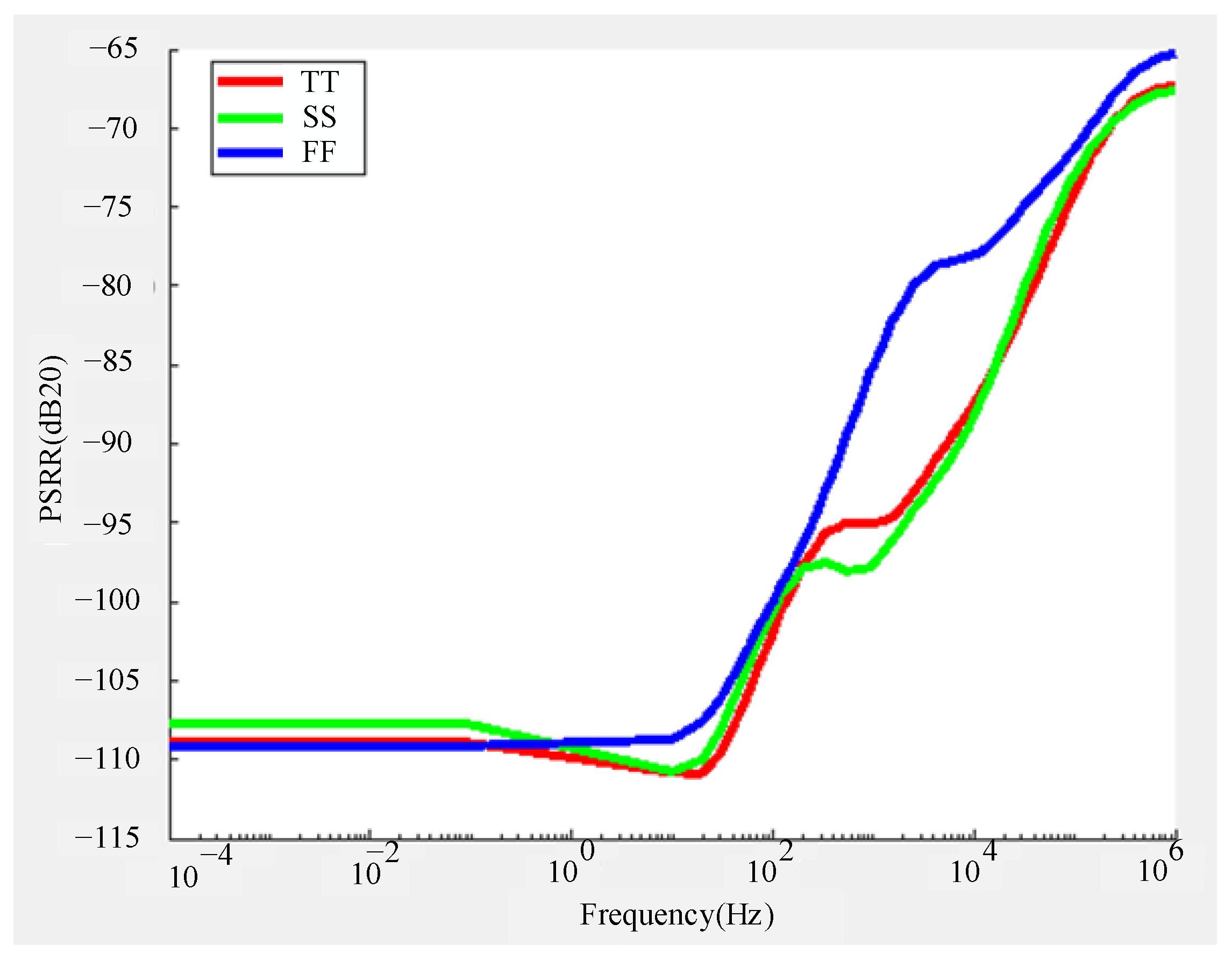
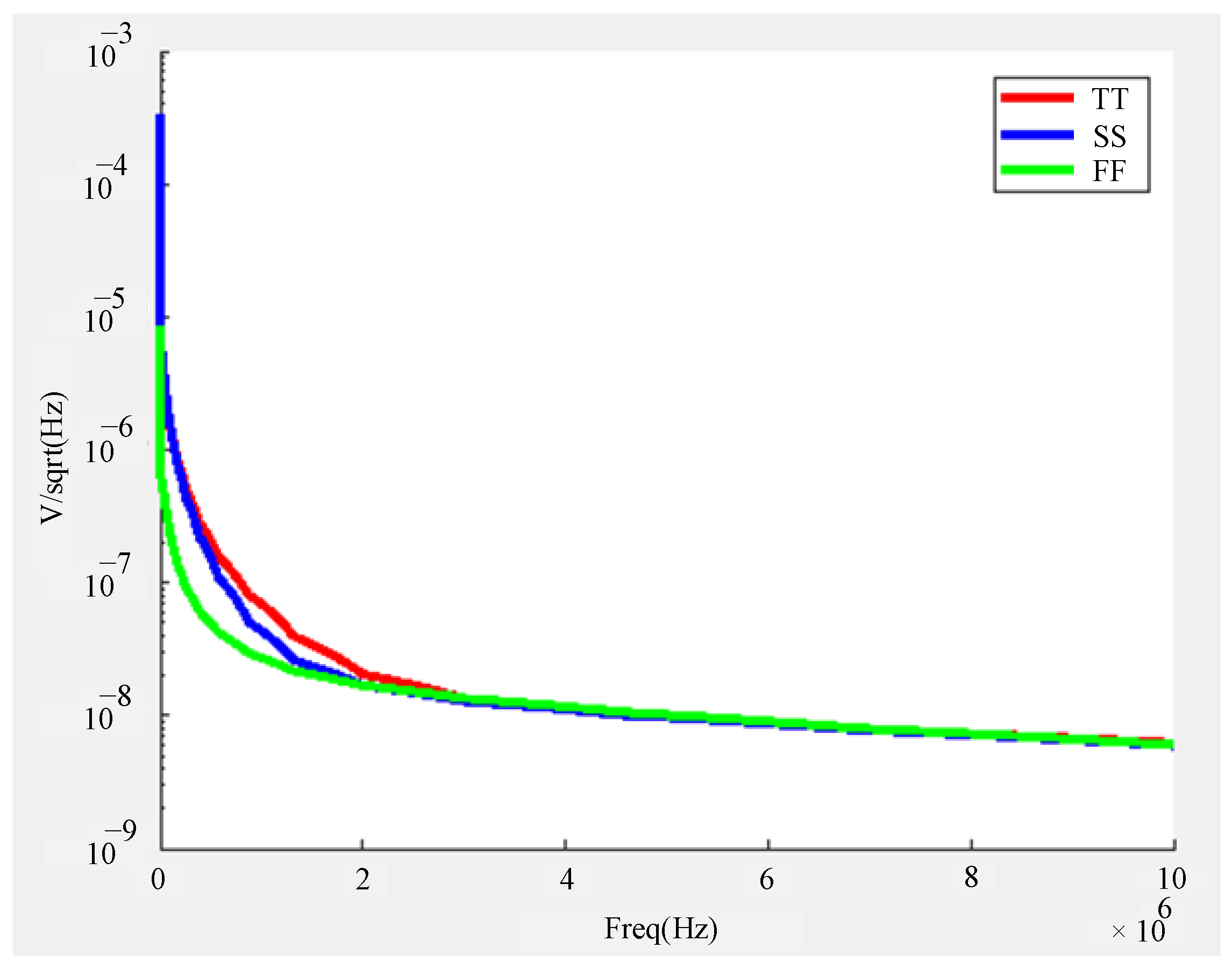
3. Results
4. Conclusions
Author Contributions
Funding
Data Availability Statement
Conflicts of Interest
References
- Liu, Q.; Zhang, B.; Zhen, S.; Xue, W.; Qiao, M. A 2.6 ppm/°C 2.5 V Piece-Wise Compensated Bandgap Reference with Low Beta Bipolar. Electronics 2019, 8, 555. [Google Scholar] [CrossRef]
- Amaljith, M.K.; Rao, G.H.; Rekha, S. Low voltage current reference circuit with low temperature coefficient. In Proceedings of the 2018 IEEE Distributed Computing, VLSI, Electrical Circuits and Robotics (DISCOVER), Mangalore, India, 13–14 August 2018; pp. 60–63. [Google Scholar] [CrossRef]
- Anushree; Kaur, J. Comparative study of Curvature Correction in CMOS Bandgap Reference Circuit. In Proceedings of the 2020 IEEE 17th India Council International Conference (INDICON), New Delhi, India, 10–13 December 2020; pp. 1–4. [Google Scholar] [CrossRef]
- Huang, C.; Zhan, C.; He, L.; Wang, L.; Nan, Y. A 0.6V Minimum-Supply, 23.5 ppm/°C Subthreshold CMOS Voltage Reference With 0.45% Variation Coefficient. IEEE Trans. Circuits Syst. II Express Briefs 2018, 65, 1290–1294. [Google Scholar] [CrossRef]
- Krolák, D.; Plojhar, J.; Horský, P. An Automotive Low-Power EMC Robust Brokaw Bandgap Voltage Reference. IEEE Trans. Electromagn. Compat. 2020, 62, 2277–2284. [Google Scholar] [CrossRef]
- Li, J.; Zhang, X.; Yu, M. A 1.2-V Piecewise Curvature-Corrected Bandgap Reference in 0.5 um CMOS Process. IEEE Trans. Very Large Scale Integr. (VLSI) Syst. 2011, 19, 1118–1122. [Google Scholar] [CrossRef]
- Annema, A.-J. Low-power bandgap references featuring DTMOS. IEEE J. Solid-State Circuits 1999, 34, 949–955. [Google Scholar] [CrossRef]
- Mothukuru, R.K.; Kumar, M.; Sahoo, B.D. A Curvature Compensated Bandgap Circuit Exploiting Temperature Dependence of β. In Proceedings of the 7th International Conference on Modern Circuits and Systems Technologies, Thessaloniki, Greece, 7–9 May 2018; pp. 509–512. [Google Scholar] [CrossRef]
- Liu, L.; Mu, J.; Zhu, Z. A 0.55-V, 28-ppm/°C 83-nW CMOS sub-BGR with ultralow power curvature compensation. IEEE Trans. Circuits Syst. I Reg. Pap. 2018, 65, 95–106. [Google Scholar] [CrossRef]
- Omprakash, A.P.; Ildefonso, A.; Tzintzarov, G.; Babcock, J.; Mukhopadhyay, R.; Cressler, J.D. Using SiGe-on-SOI HBTs to Build 300 °C Capable Analog Circuits. In Proceedings of the 2018 IEEE BiCMOS and Compound Semiconductor Integrated Circuits and Technology Symposium (BCICTS), San Diego, CA, USA, 15–17 October 2018; pp. 206–209. [Google Scholar] [CrossRef]
- Lee, C.C.; Chen, H.M.; Lu, C.C.; Lee, B.Y.; Huang, H.C.; Fu, H.S.; Lin, Y.X. A High-Precision Bandgap Reference With a V-Curve Correction Circuit. IEEE Access 2020, 8, 62632–62638. [Google Scholar] [CrossRef]
- Zhang, H.; Liu, X.; Zhang, J.; Zhang, H.; Li, J.; Zhang, R.; Chen, S.; Carusone, A.C. A Nano-Watt MOS-Only Voltage Reference With High-Slope PTAT Voltage Generators. IEEE Trans. Circuits Syst. II Express Briefs 2018, 65, 1–5. [Google Scholar] [CrossRef]
- Leung, K.N.; Mok, P. A sub-1V 15 ppm/°C CMOS bandgap voltage reference without requiring low threshold voltage device. IEEE J. Solid-State Circuits 2002, 37, 526–530. [Google Scholar] [CrossRef]
- Zhu, M.; Du, K.; Wu, T.; Song, C.; Ye, L. A 187-pW 51-ppm/°C Self-Adjusting Voltage Reference Circuit. In Proceedings of the IEEE 15th International Conference on Solid-State & Integrated Circuit Technology (ICSICT), Kunming, China, 3–6 November 2020; pp. 1–3. [Google Scholar] [CrossRef]
- Chen, H.W.; Kuo, H.L. A low power supply CMOS bandgap reference voltage generator used current differential amplifier and DTMOST diode. In Proceedings of the International Conference on Applied System Innovation (ICASI), Okinawa, Japan, 26–30 May 2016; pp. 1–2. [Google Scholar] [CrossRef]
- Wang, R.; Lu, W.; Zhao, M.; Niu, Y.; Liu, Z.; Zhang, Y.; Chen, Z. A 2.1-ppm/°C current-mode CMOS bandgap reference with piecewise curvature compensation. In Proceedings of the 2017 IEEE International Symposium on Circuits and Systems (ISCAS), Baltimore, MD, USA, 28–31 May 2017; pp. 1–4. [Google Scholar] [CrossRef]
- An, J.; Wu, C.; Xu, D. A Wide Temperature Range 4.6 ppm/°C Piecewise Curvature-Compensated Bandgap Reference With No Amplifiers. In Proceedings of the 2019 International Conference on IC Design and Technology (ICICDT), Suzhou, China, 17–19 June 2019; pp. 1–4. [Google Scholar] [CrossRef]
- Zhu, G.; Yang, Y.; Zhang, Q. A 4.6-ppm/°C High-Order Curvature Compensated Bandgap Reference for BMIC. IEEE Trans. Circuits Syst. II Express Briefs 2019, 66, 1492–1496. [Google Scholar] [CrossRef]
- Chen, H.M.; Lin, K.H.; Chen, C.C. A 1.33 ppm/°C Precision Bandgap Reference with Piecewise-Linear Curvature Compensation. In Proceedings of the IEEE International Conference on Consumer Electronics-Taiwan (ICCE-Taiwan), Taoyuan, Taiwan, 28–30 September 2020; pp. 1–2. [Google Scholar] [CrossRef]
- Amaral, W.A. A New Voltage Reference Based on Threshold Voltages Summation of CMOS Transistors. In Proceedings of the 2019 IEEE 62nd International Midwest Symposium on Circuits and Systems (MWSCAS), Dallas, TX, USA, 4–7 August 2019; pp. 149–151. [Google Scholar] [CrossRef]
- Lyu, N.; Yu, N.; Yi, M. An improved voltage bandgap reference with high-order curvature compensation. In Proceedings of the 2015 IEEE 11th International Conference on ASIC (ASICON), Chengdu, China, 3–6 November 2015; pp. 1–4. [Google Scholar] [CrossRef]
- Tan, W.D.; Gan, F.F.; Chang, T.C. Using normal quantile plot to select an appropriate transformation to achieve normality. Comput. Stat. Data Anal. 2004, 45, 610–619. [Google Scholar] [CrossRef]
- Quan, L.; Yin, Y.; Yang, X.; Deng, H. Design of a high precision band-gap reference with piecewise-linear compensation. In Proceedings of the Anti-counterfeiting, Security, and Identification, Taipei, Taiwan, 24–26 August 2012; pp. 1–5. [Google Scholar] [CrossRef]
- Pan, G.; Hua, Q.; Zhang, B. A 1.8 V 0.918 ppm/°C CMOS bandgap voltage reference with curvature-compensated. IEICE Electron. Express 2019, 16, 20190616. [Google Scholar] [CrossRef] [Green Version]


| Performance | TT | FF | SS |
|---|---|---|---|
| Simulated TC (ppm/°C) | 3.95 | 5 | 6.5 |
| PPSR@100 Hz (dB20) | −103 | −100 | −102 |
| Vnoise@100 Hz (μV) | 29 | 22.8 | 0.9 |
| Type | G. Zhu et al. [18] | L. Quan et al. [23] | G. Pan et al. [24] | This Work |
|---|---|---|---|---|
| Power supply (V) | 3.5~5 | 1.8 | 1.3~3.6 | 1.8 |
| Process (μm) | 0.18 | 0.18 | 0.18 | 0.11 |
| VREF (V) | 3.11 | 0.5 | 1 | 1.2 |
| Temperature range (°C) | −40~130 | −45~125 | −40~125 | −40~125 |
| TC (ppm/°C) | 4.6 | 2.61 | 0.918 | 3.95 |
| PPSR (dB20) | −92 | −107.2 | - | −108 |
| Power consumption (μW) | 378 | 400 | 41.4 | 7.5 |
Publisher’s Note: MDPI stays neutral with regard to jurisdictional claims in published maps and institutional affiliations. |
© 2022 by the authors. Licensee MDPI, Basel, Switzerland. This article is an open access article distributed under the terms and conditions of the Creative Commons Attribution (CC BY) license (https://creativecommons.org/licenses/by/4.0/).
Share and Cite
He, Y.; Yuan, G.; Lei, L.; Yu, H.; Kong, D. A 3.95 ppm/°C 7.5 μW Second-Order Curvature Compensated Bandgap Reference in 0.11 μm CMOS. Electronics 2022, 11, 2869. https://doi.org/10.3390/electronics11182869
He Y, Yuan G, Lei L, Yu H, Kong D. A 3.95 ppm/°C 7.5 μW Second-Order Curvature Compensated Bandgap Reference in 0.11 μm CMOS. Electronics. 2022; 11(18):2869. https://doi.org/10.3390/electronics11182869
Chicago/Turabian StyleHe, Yuefeng, Guoshun Yuan, Lei Lei, Hongjiang Yu, and Dewei Kong. 2022. "A 3.95 ppm/°C 7.5 μW Second-Order Curvature Compensated Bandgap Reference in 0.11 μm CMOS" Electronics 11, no. 18: 2869. https://doi.org/10.3390/electronics11182869
APA StyleHe, Y., Yuan, G., Lei, L., Yu, H., & Kong, D. (2022). A 3.95 ppm/°C 7.5 μW Second-Order Curvature Compensated Bandgap Reference in 0.11 μm CMOS. Electronics, 11(18), 2869. https://doi.org/10.3390/electronics11182869