Article

A Second Order 1.8–1.9 GHz Tunable Active Band-Pass Filter with Improved Noise Performances

Department of Industrial and Information Engineering, University of L’Aquila, 67100 L’Aquila, Italy
*
Author to whom correspondence should be addressed.
Electronics 2022, 11(17), 2781; https://doi.org/10.3390/electronics11172781
Submission received: 4 August 2022 / Revised: 29 August 2022 / Accepted: 1 September 2022 / Published: 3 September 2022
(This article belongs to the Special Issue Feature Papers in Circuit and Signal Processing)

Abstract

:
In this paper, a novel active tunable band-pass filter with improved noise performances is presented. This filter is based on a negative resistance circuit (or active capacitance), where the gain obtained with a transistor is used to compensate for inductor losses. Moreover, the capacitance of the resonator is obtained through a voltage-controlled reverse-biased varactor, which allows for frequency tuning. Despite the active component, the proposed filter also has good noise performance. Measurements show a tunability range from 1.816 GHz to 1.886 GHz, with a bandwidth of 38 MHz. The insertion loss maximum value is 0.4 dB, while the noise figure value has a minimum value of 2.5 dB at the center frequency within the tunability range.

1. Introduction

One of the essential components of a telecommunication system, especially for transmitters and receivers, are filters, such as harmonic suppression low-pass filters (LPF) [1] and channel selection band-pass filters (BPF) [2]. This circuit is used for a variety of different purposes and applications, and different bands and frequency ranges correspond to specific communication channels that carry information and data with specific protocols. In this way, BPFs with a narrow bandwidth are highly desirable in order to both achieve better usage of the spectrum and obtain higher spectral efficiency. Analog BPFs are commonly implemented using passive resonators, which can consist of a crystal oscillator or, especially for RF frequencies or integrated circuits, an LC resonator; however, when shrinking the circuit dimensions and raising the frequency, passive filters performances tend to degrade because of parasitic components.
The use of active elements can then be a suitable choice for losses compensations: the narrowness of a filter is strictly related to its quality factor (Q), which is due to losses and decreases as the dimensions decrease; this is unavoidable for high frequencies, which require a small value of capacitance/inductance. Since Q is proportional to the inverse of power loss, active elements can help to compensate for these losses with their gain, resulting in a higher Q and better performances [3]. These kinds of devices, referred to as active filters, have been studied for a long time, as they can solve the passive filters’ main issue, especially for high frequency applications [4].
Active components, referring to this category of filters, are equivalent to a resistance with a negative value that can compensate for losses due to dissipative parasitic elements. However, this negative resistance must be carefully evaluated because it can lead to instability and oscillation; in this case, the filter is no longer usable, also becoming a not-reciprocal network. Another issue with active filters is due to noise performances: the inherent gain stage of the active resonator can easily be responsible for an elevated noise figure, depending on the design [5]; to be competitive with passive filters, this aspect should also be taken into account.
In the literature, the main proposed solutions are based on active inductors or, as in this paper, active capacitors. The first kind involves a feedback network (typically a gyra-tor) with a transistor that emulates an inductance, removing issues typically caused by physical inductors [6,7,8,9]. Since the real inductor is removed, those filters tend to have a higher Q compared with the other topologies [10] and are suitable choices for integrated systems [11]. However, as a drawback, gyrator and other active inductance circuits usual-ly involve a significant number of components: this usually results in a higher noise figure [12], requiring sophisticated characterization strategies [13]. A large number of ele-ments also makes tuning more difficult, so that multiple tunable elements (as varactors) are needed [14] or multiple control signals with dedicated calibration systems [15]. Final-ly, a large number of components means a higher power consumption, so low-power de-vices could require low-power polarizations (i.e., class B or AB) [16] that affect linearity.
The second approach is based on active capacitors. This method uses the inherited capacitance of the transistors (both FET or junction) to replace the physical capacitor, re-sulting in a smaller number of components, gaining rising popularity [17,18,19]. In this way, both power consumption [20] and noise figure [21] are reduced compared to active induc-tor topologies. This simple circuit structure also allows an easier tunability with respect to the active inductors.
To achieve tunability, both in active inductors and in active capacitors, it is necessary to change the equivalent value of one resonant element within the filter. With gyrators, a common strategy is to change the biasing current or voltage with accuracy, in order to not affect the filter performances [22]. Another popular method is using varactors, as they provide a voltage-dependent capacitance that modifies resonating frequency [23]. The use of multiple varactors allows a more accurate frequency tuning, thus, increasing the noise figure, so a compromise must be found [24].
In this paper, we propose a tunable second order band-pass filter based on the active capacitance method. The filter peak frequency is tunable from 1.816 GHz to 1.886 GHz with a bandwidth of 38 MHz; it uses a common-emitter Hetero-junction Bipolar Transistor (HBT) as an active capacitor that gives the required value of negative resistance. Tunability and frequency tuning are achieved by using a varactor (or varicap) in parallel with the active resonator. With this configuration, the total equivalent capacitance is the sum of the transistor and the varactor, which can be changed by varying the reverse voltage across the varactor. Even if the resistance value is also affected, this contribution is minimal with respect to the value of the active circuit itself. Hence, with a single control voltage, a significant span of tunability is achieved without affecting losses compensation, and so the Q is also not significantly changed. Simulations and experimental results are reported in the following sections: measurements showed that a total insertion loss has a maximum value of 0.4 dB. Moreover, the noise figure was measured, finding values not greater than 4.2 dB within the entire frequency span of tunability.

2. Materials and Methods

2.1. Negative Resistance Theory

This section presents the working principle of a negative resistance circuit using a bipolar transistor in a common-emitter configuration with a series RLC as a load. While the reactive elements ( L c , C c ) are used to select the resonant frequency, the resistance ( R c ) is necessary to avoid instability: this load is, in fact, a feedback structure that can easily lead to oscillation; the resistance value ensures a dissipation that can reduce overall gain and ensure stability. Since there is no base-emitter or base-collector feedback, this configuration can also offer good noise performances.
The schematic and equivalent circuit of this structure is shown in Figure 1. Using the equivalent circuit in (b), the analytic expression of the input impedance of this network can be calculated as follows:
Z i n = Z b e ( Z b c + Z c ) Z b c + Z c + Z b e + g m Z b e Z c
where r 0 , C c e and h i e can be neglected due to their small contribution to the impedance calculation, being:
Z b e = j X b e = 1 j ω C b e
Z b c = j X b c = 1 j ω C b c
Z c = R c + j X c = R c + ( ω L c 1 ω C c )
where both X b e and X b c are defined as positive. Equation (1) can be rewritten in terms of a real and imaginary part, as follows:
Y i n = R c + g m ( R c 2 + ( X c X b c ) X c ) R c 2 + ( X c X b c ) 2 + j ( 1 X b e X c X b c + g m X b c R c R c 2 + ( X d X b c ) 2 ) = G i n + j ω B i n
Considering R c = 0   Ω and X c > 0 (i.e., the load is inductive), we can find the frequency range in which G i n (and so R i n ) is negative; this is within the two frequencies f m i n and f m a x , that can be evaluated as:
f m i n = 1 2 π L c C c
f m a x = 1 2 π L c C m a x  
being C m a x the equivalent series capacitance of C b c and C c , given by:
C m a x = C b c C c C b c + C c
From Equation (5) we can see that the series resistance R c to the feedback has two main consequences: the frequency range in which the real part is negative is reduced, and its maximum value is reduced too. The resistance is also fundamental for stability as a damping element because of the feedback structure of the active cell that can cause instability due to its positive gain; a good value of resistance can dissipate enough power to avoid oscillation and positive feedback. As a consequence, a compromise between damping and gain must be chosen as a value for R c .

2.2. Losses Compensation and Frequency Tuning

Since values for the feedback load must be chosen to set the proper frequency range of the negative resistance and its maximum value, the active capacitance itself does not have enough degrees of freedom to make the equivalent capacitance equal to the capacitance of the resonator. Consequently, to use it in a filter, it is necessary to change that value to the desired one. Moreover, the active cell needs to be decoupled from the circuit to be correctly biased, so a series capacitor is also required. The resulting structure behaves like a tapped capacitor with negative resistance, as shown in Figure 2a. In order for a negative resistance to compensate for the losses of the resonator, its conductance value must be equal in absolute value to the equivalent parallel resistance of a real inductor. To achieve this, the values of the tapped capacitors ( C b and C p ) must be defined by evaluating the equivalent value of resistance and capacitance that match the resonator design parameters, as in Figure 2b.
The value of R l o s s is related to the equivalent series resistance (ESR) of the inductor and can be well approximated by the equation:
R l o s s Q 2 E S R = ω 0 L Q
where Q is the quality factor of the inductor, that is Q = ω 0 L E S R . This resistance is the value that is desired with the opposite sign as the input resistance of the active capacitor, so that the total equivalent conductance with respect to ground is equal to zero and the effective resonator is purely reactive, with a resonant frequency equal to:
ω 0 = ( L r e s C r e s ) 1 2
being L r e s the value of the inductor and C r e s the input capacitance of the tapped capacitors with the active one. To obtain those values of resistance and impedance from the negative resistance circuit, its input admittance can be written as follows:
Y e q = ω 2 R i n [ C p ( C b + C i n ) C b C i n ] + j ω [ C p + C b + ω 2 R i n 2 ( C p ( C b + C i n ) 2 + C b C i n ( C b + C i n ) ) ] 1 + ω 2 R i n 2 ( C b + C i n ) 2
If we assume both Q 1 2 = ω 2 R i n 2 ( C b + C i n ) 2 , Q 2 2 = Q 1 C p C p + C b and Q 3 2 = Q 1 C b C i n ( C b + C i n ) ( C p + C b ) in order to be Q 1 2 ,   Q 2 2 , Q 3 2 1 , then the input admittance real and imaginary part can be expressed as:
G e q 1 R i n ( C b C b + C i n )
C e q C p + C b C i n C b + C i n
Previous equations permit finding the value of C b and C p by assuming G e q = 1 R l o s s and C r e s = C e q . However, if the relation Q 1 2 ,   Q 2 2 , Q 3 2 1 is not satisfied, those values can be a starting point to optimize the correct one, as they give two degrees of freedom to adjust the cell inductance.
A varactor connected in parallel to the resonant cell allows a change of the equivalent capacitance, hence, the resonating frequency, while its effect on dissipation can be neglected since it is reverse biased, showing a high resistance. However, it is necessary to employ a bypass capacitor to avoid the DC current interfering with the RF signal; its value must be at least comparable to the minimum value of the varactor, as a smaller value would reduce and eliminate tunability. Moreover, it must be noted that a variation of the total capacitance changes the value of the negative resistance, so that far from the starting frequency losses, compensation would be less effective; regardless, choosing a wide “negative range”, the resistance value is flat enough to ensure tunability without significative differences in the quality factor of the filter.

2.3. Performance Evaluation

To evaluate the performance of both the simulated and measured prototype of the filter with the proposed design technique, the IL and the Q factor of the filter were evaluated using the Scattering parameters, according to the following equations:
IL = 20 log S 21
Q l = f 0 f 3 d B
where Q l is the loaded Q of the filter, considering a load and a source impedance of 50 Ω. The noise figure (NF) was also evaluated, expressed in dB.

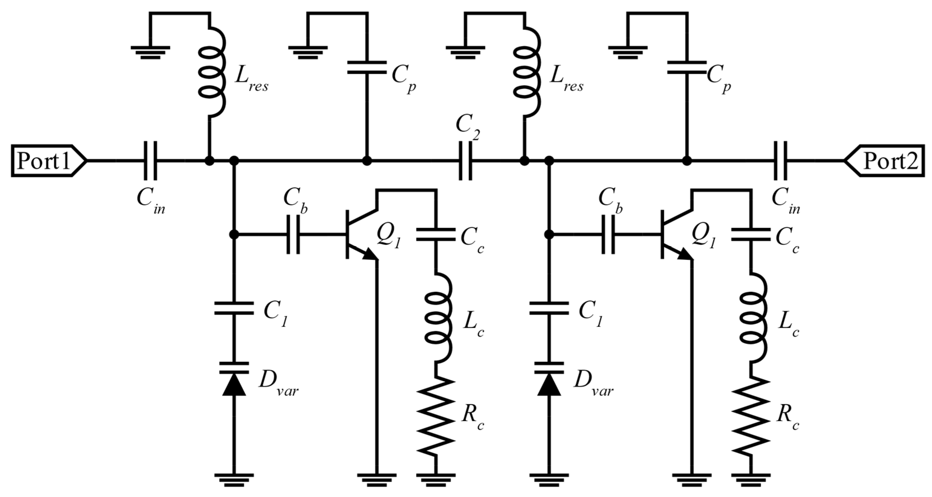
3. Design and Simulations

3.1. Filter Design Method

Starting with the above-written equations, we designed an active filter, adjusting and optimizing the simulated values, keeping count of the non-idealities of real components and microstrip lines, as explained further in this section. All the simulations were carried out on Cadence’s software AWR Design Environment.
First, a passive band-pass filter was designed following the Cohn’s coupled resonators filter topology [25] to find the values of capacitance C r e s and inductance L r e s required, in which the inductor value was established according to the commercial chip inductors available; this allowed for evaluating the behavior of the filter using an inductor with a specific Q, considering the introduced losses. Then, values for the RLC feedback load were chosen, using Equations (6) and (7), to ensure that the negative impedance was within the interested frequency range, considering the damping resistance equal to zero; since this range shrinks as the resistance becomes larger, it must be greater than the desired tunability range. Once the values for the feedback load and the resonator parameters were set, we needed to match the active capacitance input admittance with the desired one to achieve the equivalent parallel resistance of the chosen real inductor, which is R l o s s in (9), so that the input resistance and the input capacitance of the active circuit matched R l o s s and C r e s , respectively. To achieve this, from (12) and (13), we found out the starting values for C p and C b , optimizing them on the AWR software. With the resonators value decided, we also added the damping resistor to make the S21 of the filter smaller than 0 dB (i.e., to avoid filter instability and oscillations).
Since we aim for a tunable filter, we replaced C p with a reverse-biased varactor; as in (12) and (13), its main contribution is given to the equivalent capacitance, while the resistance (which is responsible for dissipation compensation) is not affected.
Tuning voltage is given to the varactor through a resistor that must be great enough to avoid interferences with the RF signal, and it is also decoupled with the signal path with a bypass capacitor. The schematic of the final design (without biasing networks) is reported in Figure 3.
Since we introduced microstrips to realize the filter, these initial values needed to be modified and optimized to maintain the same performances. The use of non-ideal lines introduced parasitic inductance so that the capacitive values, in general, needed to be increased, while the inductive ones needed to be reduced. This procedure allowed us to obtain a coupled resonator filter with tunable active resonators. The length of the lines was dimensioned, simulating the circuit behavior on AWR Design Environment by Cadence.

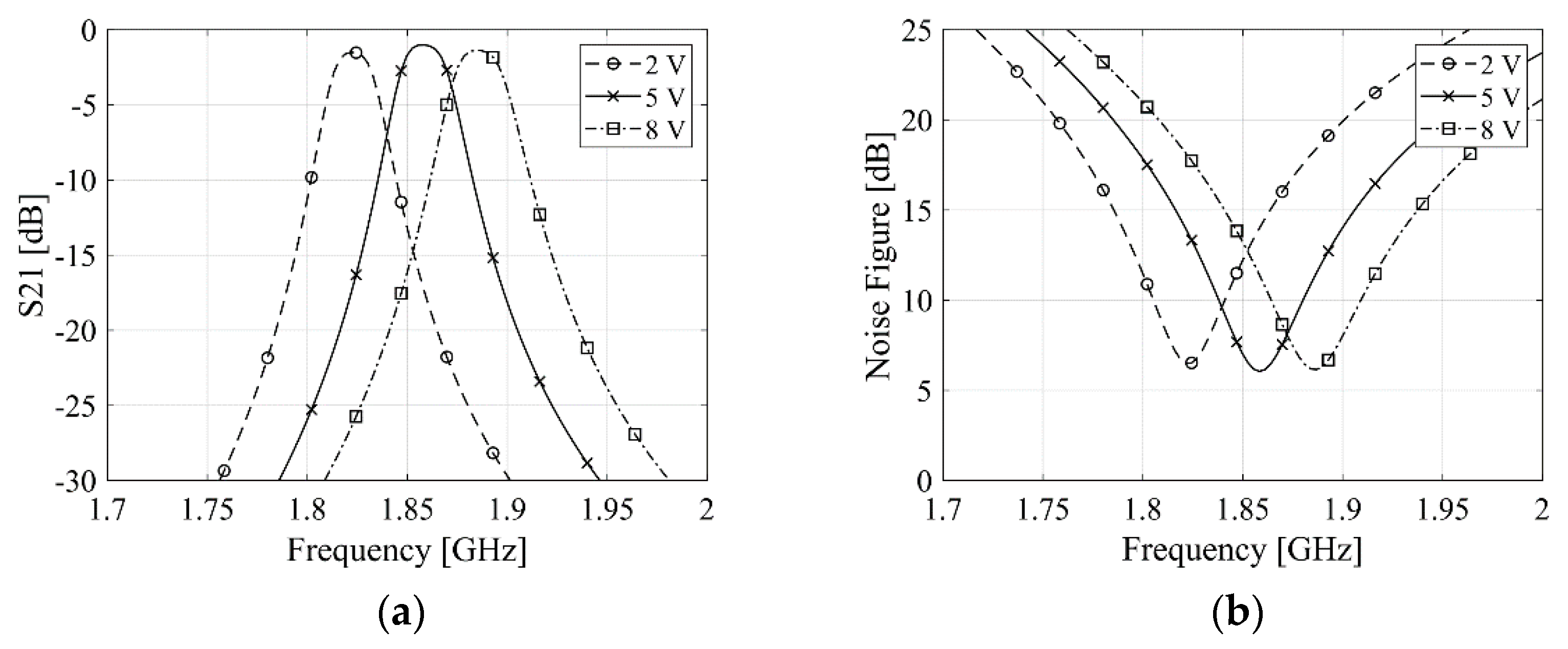
3.2. Simulation Analysis

The filter performance was simulated using the S-parameters equivalent model of the used components to evaluate the filter’s frequency response and verify its tunability. Figure 4 shows the value of the simulated S21 for three different values of tuning voltage. The insertion loss so obtained is smaller than 1 dB within all the tuning ranges. The obtained bandwidth is 26 MHz, 28 MHz, and 30 MHz for the three peak frequencies of 1.822 GHz, 1.857 GHz, and 1.885 GHz, respectively: hence, from these simulations, the quality factor Q of the filter ranges between 70 and 63 within the tuning band. Moreover, the noise figure at the peak frequency is not greater than 6.5 dB within the whole range, which is lower than typical active inductor active filters.
The final values of the components used for the filter are displayed in Table 1.

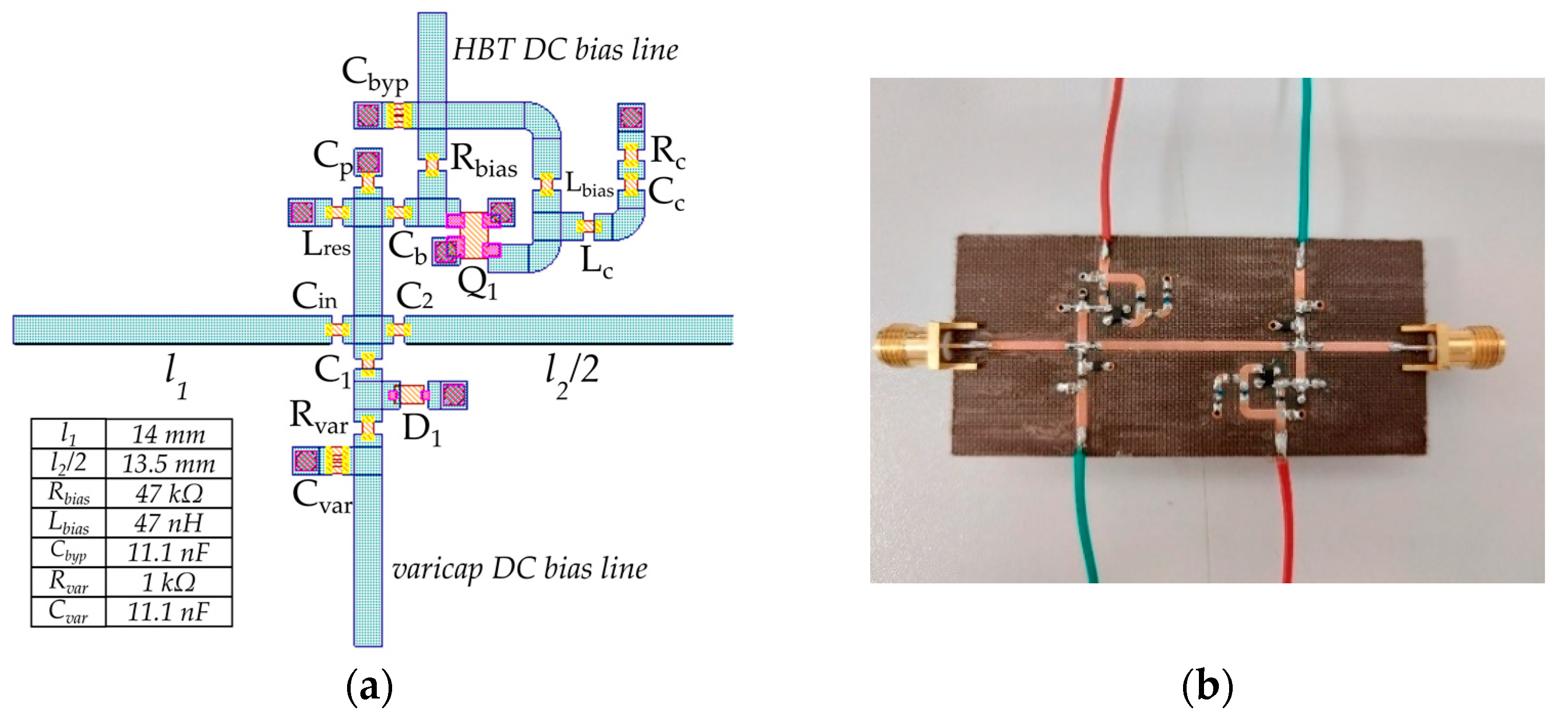
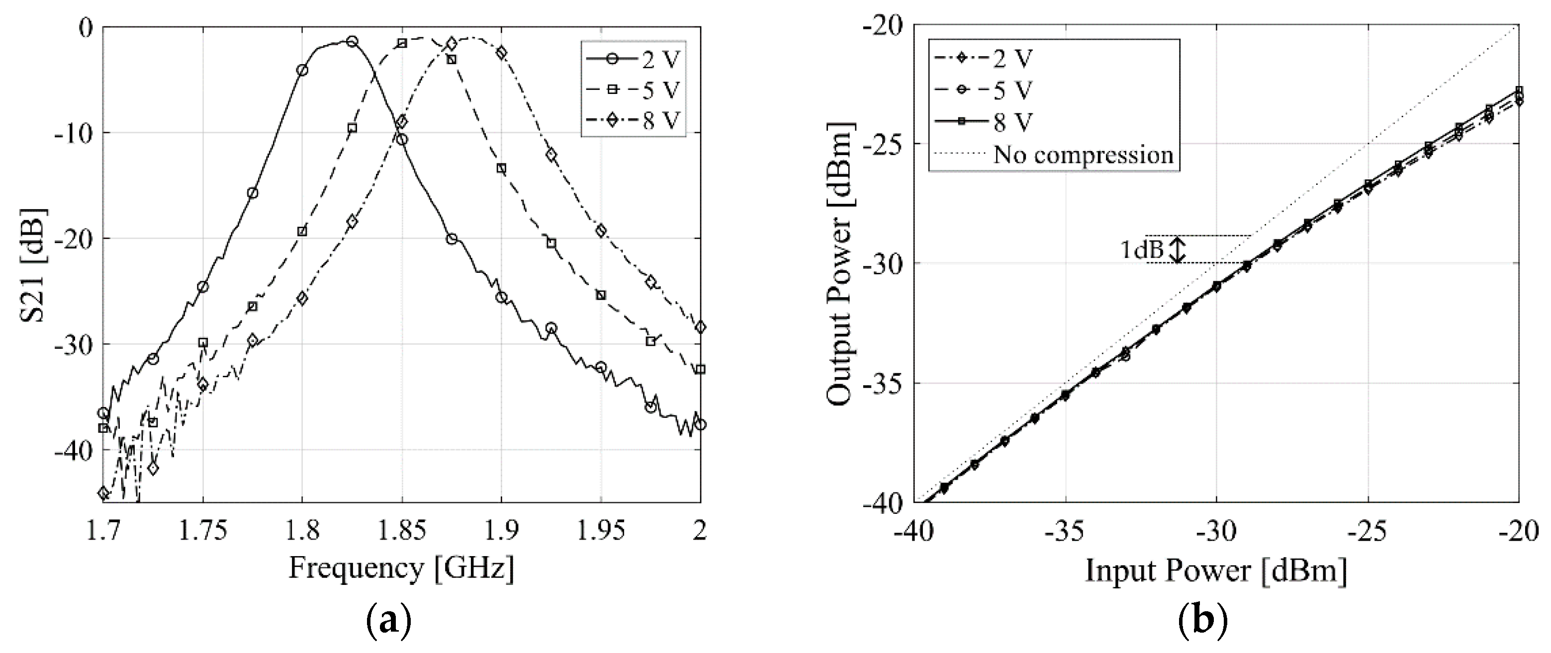
4. Measurements and Results

The designed filter (shown in Figure 5) was realized using a TLX8 substrate by Taconic that has a dielectric constant ϵ = 2.55 and a loss tangent tan δ = 0.0019 . The S parameters of the designed filter were measured for the same tuning voltages (2 V, 5 V, 8 V) of the simulations reported in Figure 4, with −30 dBm of input power. The measurement results are shown in Figure 6a. The measured filter has a maximum in-band insertion loss of 0.4 dB at 1.816 GHz, for a tuning voltage of 2 V. Peak frequencies are, respectively, 1.816 GHz, 1.86 GHz, and 1.886 GHz, so a good passband is obtained from 1.799 GHz to 1.905 GHz. The quality factor has its best for 2 V of tuning voltage, with a 38 MHz bandwidth and Q equal to 49. This slightly decreases for higher frequencies: for 5 V the bandwidth is 40 MHz, and for Q this is 46, while for an 8 V bandwidth it is 43 MHz and Q is 44. A comparison between other proposed filters is reported in Table 2; the Shape Factor showed is evaluated as the ratio between the BW−30dB and the BW−3dB.
Measurements showed a small disagreement with simulations, especially for what concerns the bandwidth: this may be due to the parasitics of the used commercial components. A smaller bandwidth can be obtained by increasing the biasing current, though resulting in a positive S21 and deteriorating noise performances. Moreover, even if S21 is worse at lower bias currents, S11 has noticeable improvements. Finally, an analysis of the compression point is reported in Figure 6b displaying the −1 dB compression point for input power around −29 dBm for each tuning voltage. The minimum noise figure value has also been measured for the same tuning voltages, obtaining values of 4.2 dB, 3.28 dB, and 2.5 dB, respectively.

5. Conclusions

In this paper, a frequency-tunable active filter based on active capacitance was presented, with a tunable bandwidth that ranges from 1.799 GHz up to 1.905 GHz. The active capacitance method was used to compensate for losses due to the parasitics of the inductor present in the resonator. We observed that the main effect on both frequency response and insertion loss is related to the feedback network of the active component. Moreover, we observed that fine frequency tuning could be obtained with the use of varactors, while a good gain control is feasible using a variable resistor on the feedback network, hence, damping each possible resonance. Filter performances maintain a similar behavior for each center frequency within the tunability range, controlling the capacitance of the varactor without modifying the active circuitry. The active capacitance approach also showed good noise performances, with a minimum noise figure of 2.5 dB, thanks to the small number of active devices. This kind of active filter creates high flexibility in the design and in optimization, allowing for the control of a restricted number of parameters to suit various different applications.

Author Contributions

Conceptualization, V.S., A.L. and D.C.; methodology, A.L. and D.C.; software, D.C.; validation, V.S., G.F. and A.L.; formal analysis, D.C. and A.L.; investigation, D.C.; resources, V.S.; data curation, A.L. and D.C.; writing—original draft preparation, D.C.; writing—review and editing, A.L. and G.F.; supervision, A.L. and G.F.; project administration, V.S.; All authors have read and agreed to the published version of the manuscript.

Funding

This research received no external funding.

Institutional Review Board Statement

Not applicable.

Informed Consent Statement

Not applicable.

Data Availability Statement

The data presented in this study are available in the article.

Acknowledgments

We thank Andrea Pelliccione (University of L’Aquila) for the technical support and prototype fabrication.

Conflicts of Interest

The authors declare no conflict of interest.

References

  1. Roshani, S.; Dehghani, K.; Roshani, S. A Lowpass Filter Design Using Curved and Fountain Shaped Resonators. Frequenz 2019, 73, 267–272. [Google Scholar] [CrossRef]
  2. Tsividis, Y.P. Integrated continuous-time filter design—An overview. IEEE J. Solid-State Circuits 1994, 29, 166–176. [Google Scholar] [CrossRef]
  3. Adams, D.K.; Ho, R.Y.C. Active Filters for UHF and Microwave Frequencies. IEEE Trans. Microw. Theory Tech. 1969, 17, 662–670. [Google Scholar] [CrossRef]
  4. Snyder, R.V.; Bozarth, D.L. Analysis and Design of a Microwave Transistor Active Filter. IEEE Trans. Microw. Theory Tech. 1970, 18, 2–9. [Google Scholar] [CrossRef]
  5. Cheng, L.-K.M.; Chan, H.-Y. Noise performance of negative-resistance compensated microwave band-pass filters. Theory and experiments. IEEE Trans. Microw. Theory Tech. 2001, 49, 924–927. [Google Scholar] [CrossRef]
  6. Thanachayanont, A. Low voltage low power CMOS inductorless RF band-pass filter with high image rejection capability. In Proceedings of the 2002 45th Midwest Symposium on Circuits and Systems (MWSCAS), Tulsa, OK, USA, 4–7 August 2002. [Google Scholar] [CrossRef]
  7. Pantoli, L.; Stornelli, V.; Leuzzi, G. RF active circuit simulating a floating inductance. In Proceedings of the 2015 Integrated Nonlinear Microwave and Millimetre-Wave Circuits Workshop (INMMiC), Taormina, Italy, 1–2 October 2015. [Google Scholar] [CrossRef]
  8. Jarjar, M.; El Ouazzani, N. Design of an OTA-based microwave active band-pass filter. In Proceedings of the 2017 International Conference on Wireless Technologies, Embedded and Intelligent Systems (WITS), Fez, Morocco, 19–20 April 2017. [Google Scholar] [CrossRef]
  9. Hu, F.; Mouthaan, K. A high-selectivity active band-pass filter using gyrator based resonators in 0.13-μm CMOS. In Proceedings of the 2014 IEEE International Wireless Symposium (IWS), Xi’an, China, 24–26 March 2014. [Google Scholar] [CrossRef]
  10. Selvathi, D.; Pown, M. Design of Band Pass Filter using active inductor for RF receiver front-end. In Proceedings of the 2014 International Conference on Communication and Network Technologies, Sivakasi, India, 18–19 December 2014. [Google Scholar] [CrossRef]
  11. Stornelli, V.; Pantoli, L.; Leuzzi, G.; Leoni, A. An assessment on low-voltage low-power integrated single transistor active inductor design for RF filter applications. In Proceedings of the 2016 International Conference on IC Design and Technology (ICICDT), Ho Chi Minh City, Vietnam, 27–29 June 2016. [Google Scholar] [CrossRef]
  12. Liang, K.-H. CMOS RF Band-Pass Filter Design Using the High Quality Active Inductor. IEICE Trans. Electron. 2005, 88, 2372–2376. [Google Scholar] [CrossRef]
  13. Leoni, A.; Stornelli, V.; Pantoli, L.; Leuzzi, G.; Marinkovic, Z. RF Active Inductors Small-Signal Design by Means of Conformal Transformations. IEEE Access 2020, 8, 50390–50398. [Google Scholar] [CrossRef]
  14. Andriesei, C.; Goras, L.; Delacressoniere, B. Active RF band-pass filter with wide frequency tuning range. In Proceedings of the 2008 International Semiconductor Conference, Sinaia, Romania, 13–15 October 2008. [Google Scholar] [CrossRef]
  15. Leoni, A.; Pantoli, L.; Stornelli, V.; Leuzzi, G.; Marinković, Z. Automated Calibration System for RF Configurable Voltage-Controlled Filters. IEEE Trans. Circuits Syst. II Express Briefs 2018, 65, 1034–1038. [Google Scholar] [CrossRef]
  16. Pantoli, L.; Stornelli, V.; Leuzzi, G. Class AB gyrator-based active inductor. In Proceedings of the 2015 Integrated Nonlinear Microwave and Millimetre-Wave Circuits Workshop (INMMiC), Taormina, Italy, 1–2 October 2015. [Google Scholar] [CrossRef]
  17. Sabaghi, M.; Kouchaki, M.; Rostami, A.; Shamsoskouie, H.; Rahnama, M. Design and simulation of low-noise band-pass filter by using active capacitance circuit. In Proceedings of the 2012 IEEE 8th International Colloquium on Signal Processing and Its Applications, Malacca, Malaysia, 23–25 March 2012. [Google Scholar] [CrossRef]
  18. Il-Soo, K.; Young-Hoon, C.; Sang-Won, Y. Analysis of a novel active capacitance circuit using BJT and its application to RF band-pass filters. In Proceedings of the IEEE MTT-S International Microwave Symposium Digest, Long Beach, CA, USA, 17 June 2005. [Google Scholar] [CrossRef]
  19. Lee, J.-R.; Chun, Y.-H.; Yun, S.-W. A novel band-pass filter using active capacitance. In Proceedings of the IEEE MTT-S International Microwave Symposium Digest, Philadelphia, PA, USA, 8–13 June 2003. [Google Scholar] [CrossRef]
  20. Cho, Y.-H.; Hong, S.-C.; Kwon, Y.-S. A low-power monolithic GaAs FET band-pass filter based on negative resistance technique. IEEE Microw. Guided Wave Lett. 1998, 8, 161–163. [Google Scholar] [CrossRef]
  21. Chun, Y.-H.; Lee, J.-R.; Yun, S.-W.; Rhee, J.-K. Design of an RF low-noise band-pass filter using active capacitance circuit. IEEE Trans. Microw. Theory Tech. 2005, 53, 687–695. [Google Scholar] [CrossRef]
  22. Andriesei, C.; Goras, L.; Temcamani, F.; Delacressoniere, B. CMOS RF active inductor with improved tuning capability. In Proceedings of the 2009 International Semiconductor Conference, Sinaia, Romania, 12–14 October 2009. [Google Scholar] [CrossRef]
  23. Trabelsi, H.; Cruchon, C. A varactor-tuned active microwave band-pass filter. IEEE Microw. Guided Wave Lett. 1992, 2, 231–232. [Google Scholar] [CrossRef]
  24. Kobayashi, K.W.; Tran, L.T.; Umemoto, D.K.; Oki, A.K.; Streit, D.C. A 6.45 GHz active band-pass filter using HBT negative resistance elements. In Proceedings of the GaAs IC Symposium. IEEE Gallium Arsenide Integrated Circuit Symposium. 20th Annual. Technical Digest 1998, Atlanta, GA, USA, 1–4 November 1998. [Google Scholar] [CrossRef]
  25. Cohn, S. Direct-Coupled-Resonator Filters. Proc. IRE 1957, 45, 187–196. [Google Scholar] [CrossRef]
  26. Georgescu, B.; Finvers, I.G.; Ghannouchi, F. 2 GHz rmQ-Enhanced Active Filter with Low Passband Distortion and High Dynamic Range. IEEE J. Solid-State Circuits 2006, 41, 2029–2039. [Google Scholar] [CrossRef]
  27. Gao, Z.; Ma, J.; Yu, M.; Ye, Y. A Fully Integrated CMOS Active Bandpass Filter for Multiband RF Front-Ends. IEEE Trans. Circuits Syst. II Express Briefs 2008, 55, 718–722. [Google Scholar] [CrossRef]
  28. Wu, B.; Chiu, Y. A 40 nm CMOS Derivative-Free IF Active-RC BPF with Programmable Bandwidth and Center Frequency Achieving over 30 dBm IIP3. IEEE J. Solid-State Circuits 2015, 50, 1772–1784. [Google Scholar] [CrossRef]
Figure 1. Negative resistance circuit: (a) schematic; (b) simplified equivalent circuit used for impedance calculations; (c) complete equivalent circuit with neglected parameters.
Electronics 11 02781 g001
Figure 2. (a) Tapped capacitance and (b) its equivalent in the resonator with losses compensation.
Electronics 11 02781 g002
Figure 3. Schematic of the designed 2nd order active filter without biasing.
Electronics 11 02781 g003
Figure 4. (a) S21 and (b) noise figure simulation results for different values of tuning voltage.
Electronics 11 02781 g004
Figure 5. (a) Layout of a single cell and (b) realized 2nd order filter on TLX8 substrate; the two cells are symmetrical. Values not shown are reported in Table 1.
Electronics 11 02781 g005
Figure 6. (a) Measured S21 of the designed filter for 2 V, 5 V, and 8 V of tuning voltage; (b) output power versus input power for the same tuning voltages.
Electronics 11 02781 g006
Table 1. List of the used components for the proposed filter.
IDValueComponent
Cin0.2 pFGJM0225C1CR20WB01
Lres1.6 nHLQP03HQ1N6W02
C10.8 pFGRM1555C1HR80BA01
C2 0.2   pF   0.2 pF seriesGJM0225C1CR20WB01
Cb0.8 pFGRM1555C1HR80BA01
Cp0.5 pFGRM1555C1HR50CZ01
Cc2.7 pFGRM1555C1H2R7CZ01
Lc4.7 nHLQW15AN4N7C00
Rc5 Ω-
Q1NABFP840ESD
DvarNABBY51-W03
Table 2. Performances comparison for different filters.
Ref[5][13][12][26][27][28]This Work
TipologyActive capacitorActive inductorActive inductorActive inductorActive inductorActive RCActive capacitance
Center Frequency900 MHz0.73 GHz3.45–3.6 GHz2.03 GHz2.44 GHz0.14 GHz1.799–1.905 GHz
Bandwidth41 MHz50 MHz418 MHz *130 MHz60 MHz7–56 MHz38–43 MHz
Gain0 dB−2.5 dBn.a.06 dB0–20 dB 0.4 dB
Noise Figure min.6.1 dBn.a.14 dB15 dB18 dB34–55 dB2.5 dB
Shape Factor *5.02>12.5n.a.3.07>21.32.2–2.45.11–4.43
TechnologyGaAs MESFETdiscrete0.18 µm CMOS0.18 µm CMOS0.18 µm CMOS40 nm CMOSdiscrete
* Extracted values.
Publisher’s Note: MDPI stays neutral with regard to jurisdictional claims in published maps and institutional affiliations.

