
Machine-Learning-Based Compact Modeling for Sub-3-nm-Node Emerging Transistors


Abstract
:1. Introduction
1.1. Related Work
1.2. Contributions
1.3. Paper Organization
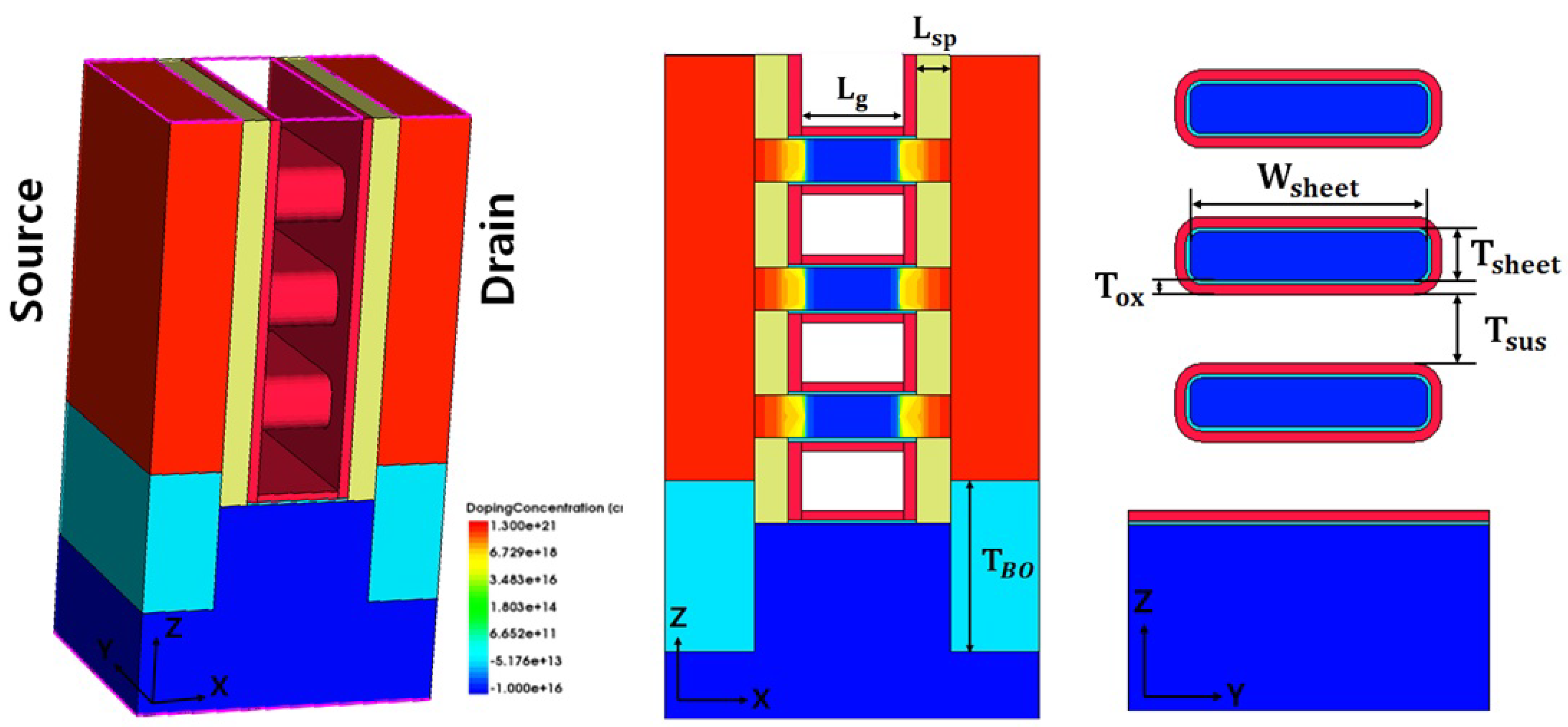
2. Device Design and Dataset Generation
2.1. Process Flow of the Nanosheet FET (NSFET)
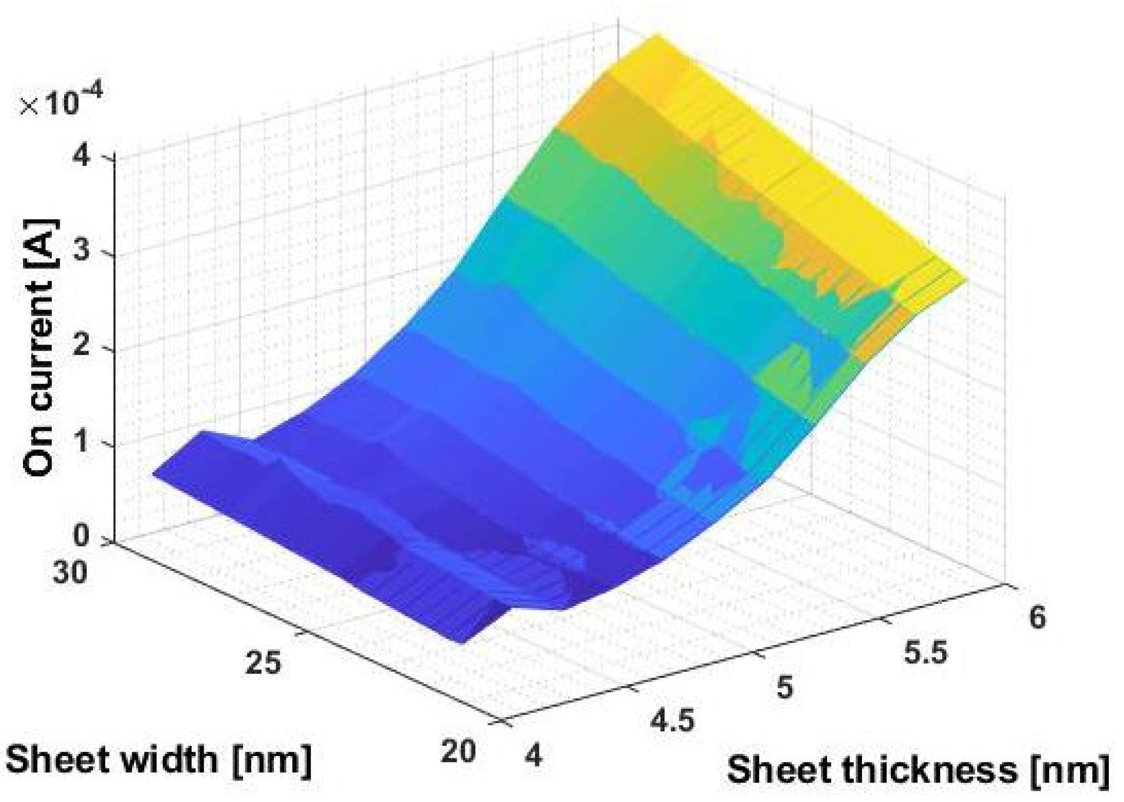
2.2. Construction of Device Datasets
2.3. Simulation Conditions
2.4. Construction of Device Datasets
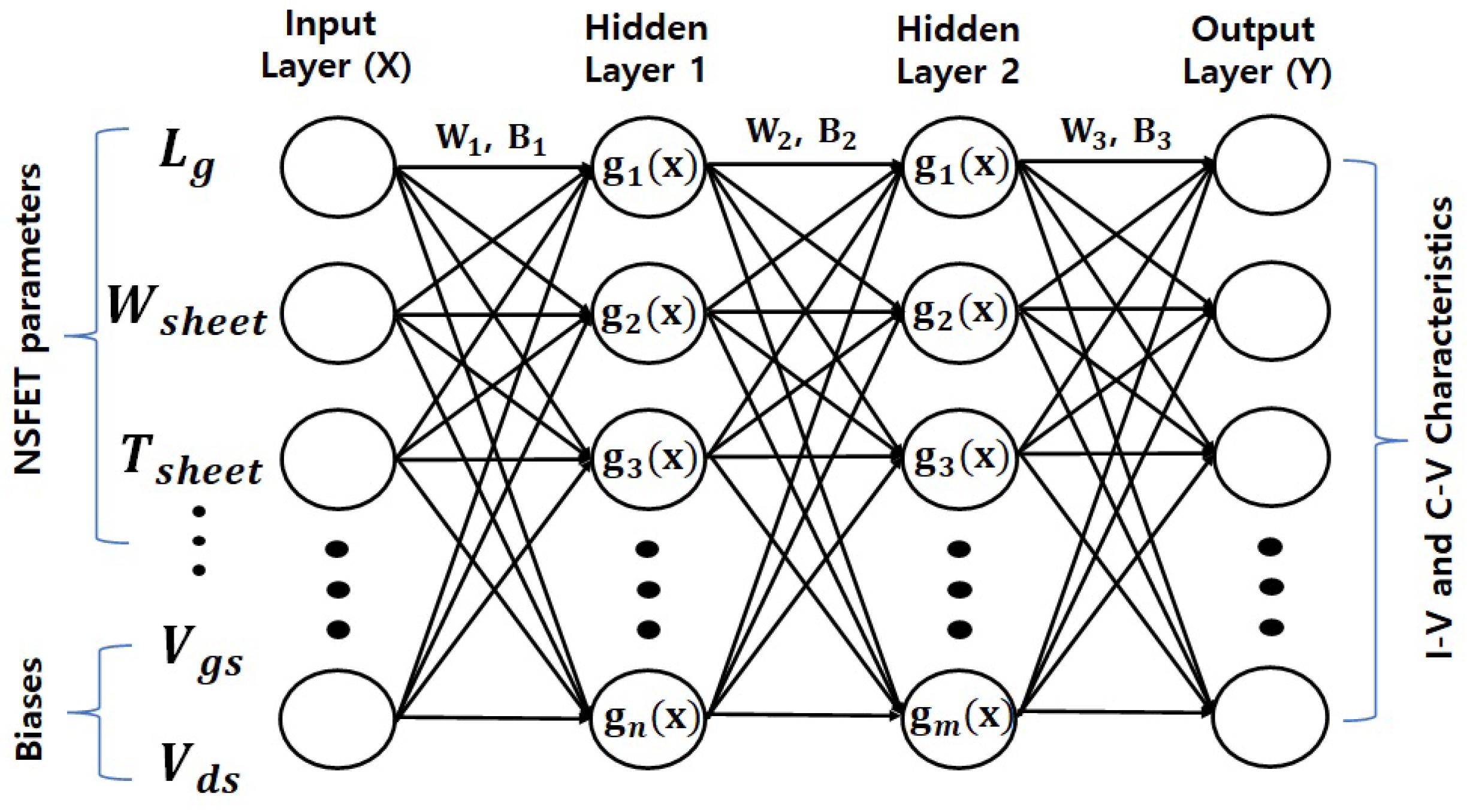
3. ANN Model Architecture and Methodology
3.1. The Architecture of the Proposed ANN Model
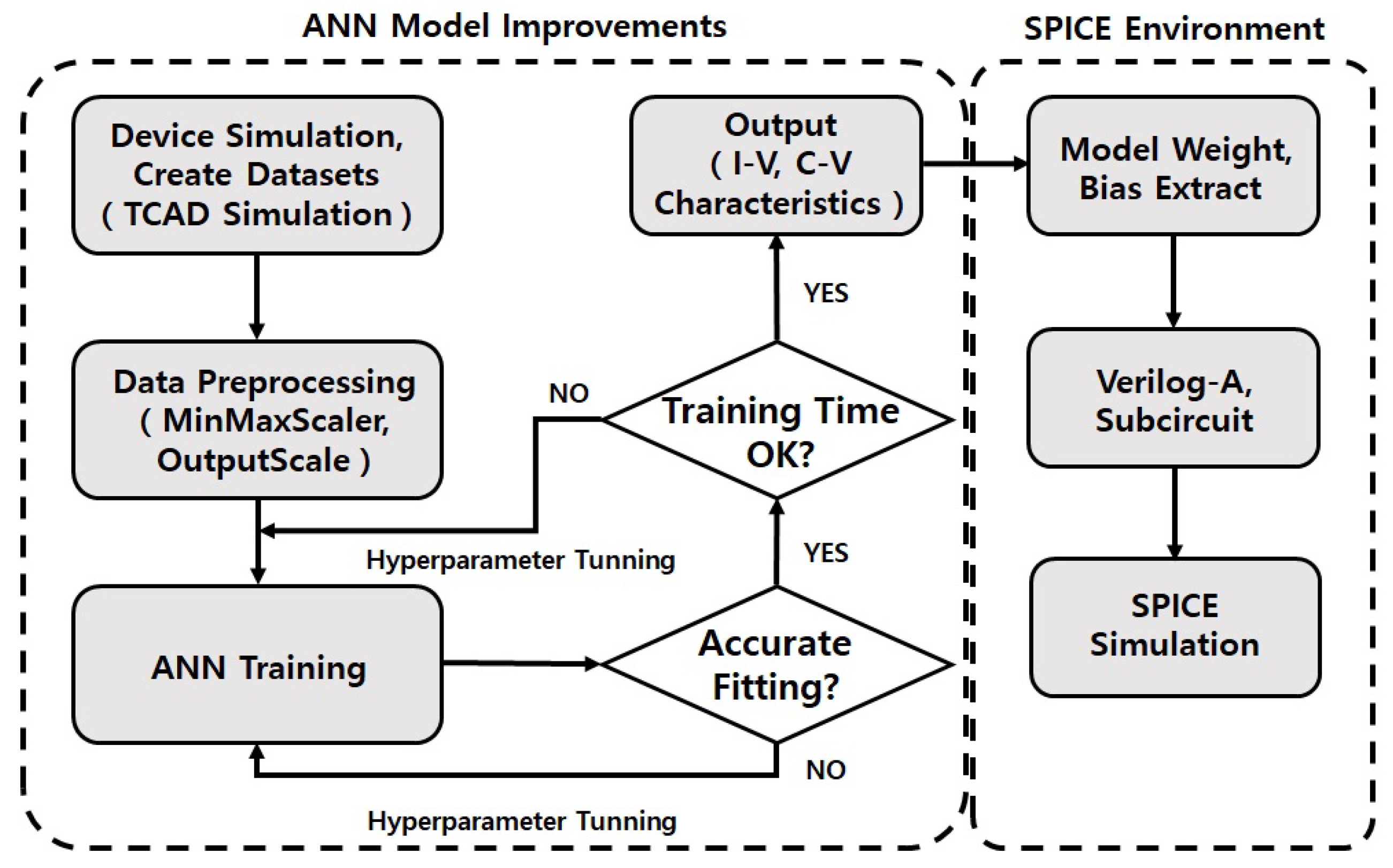
3.2. The Workflow of the ANN Model
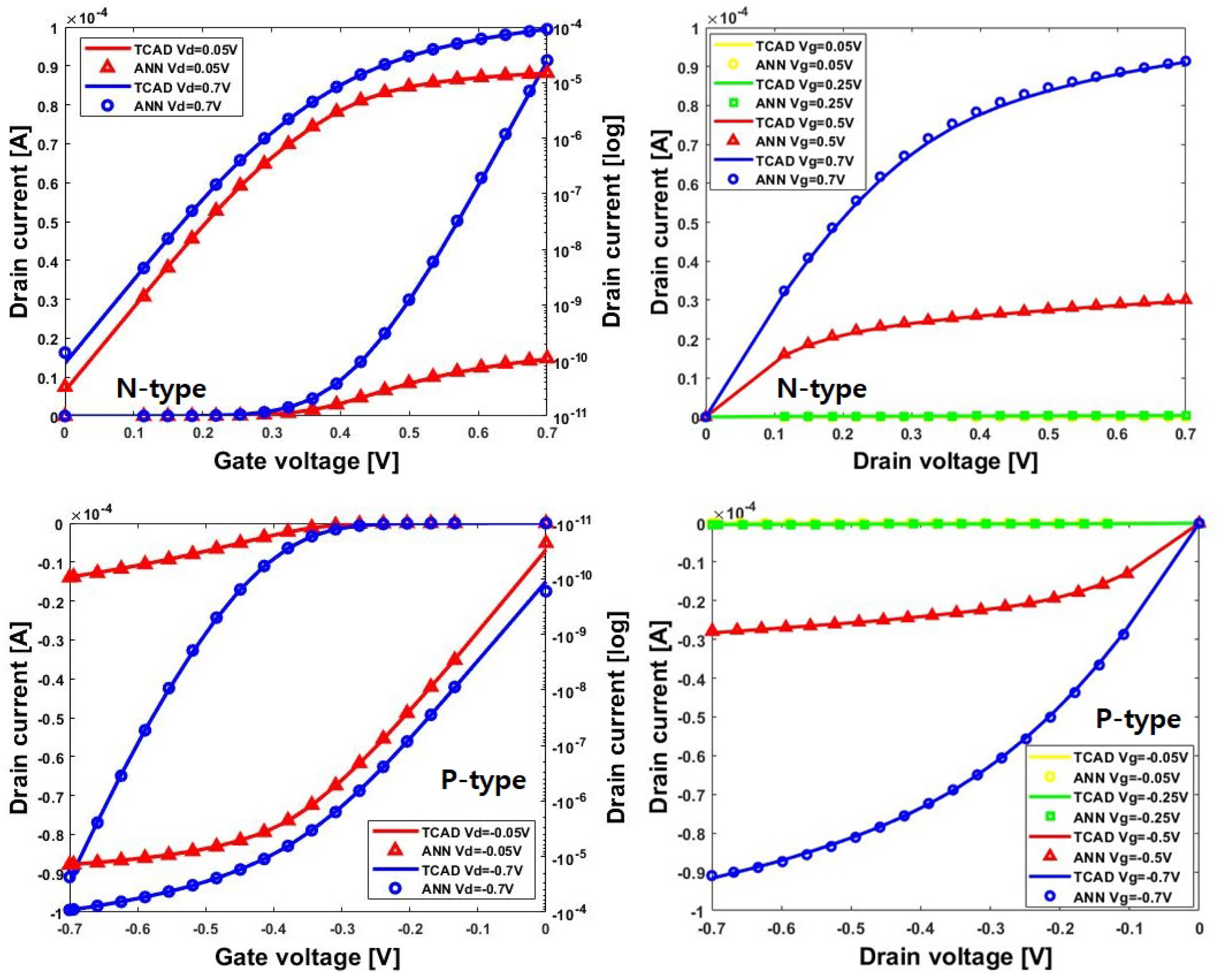
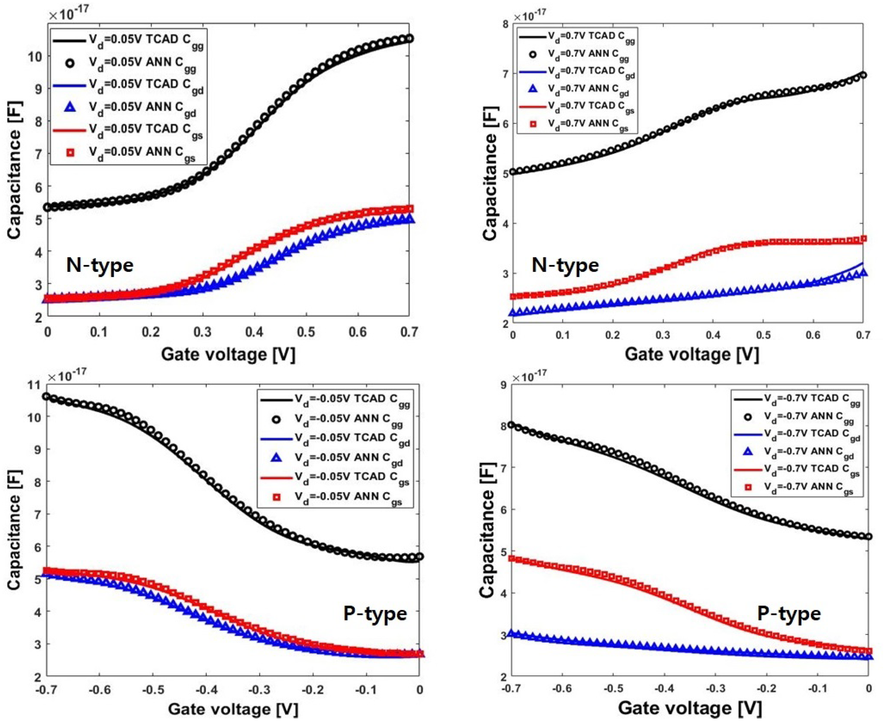
4. ANN Model Training and Results
5. SPICE Simulation of Circuits Using the Developed ANN Models
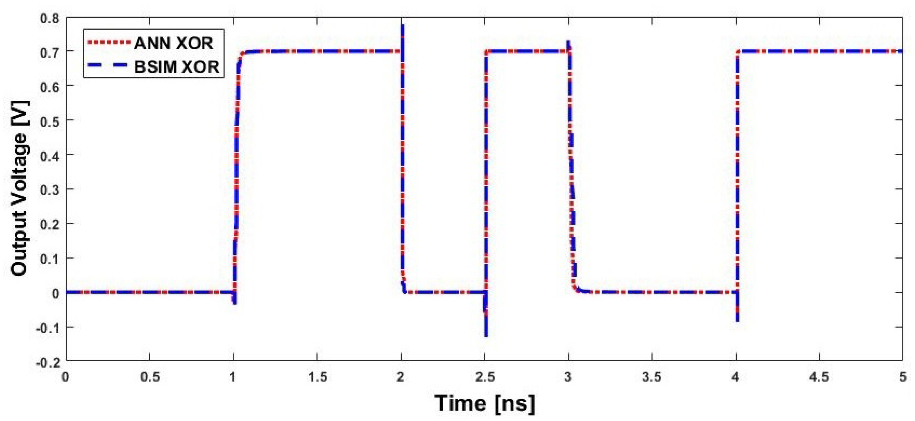
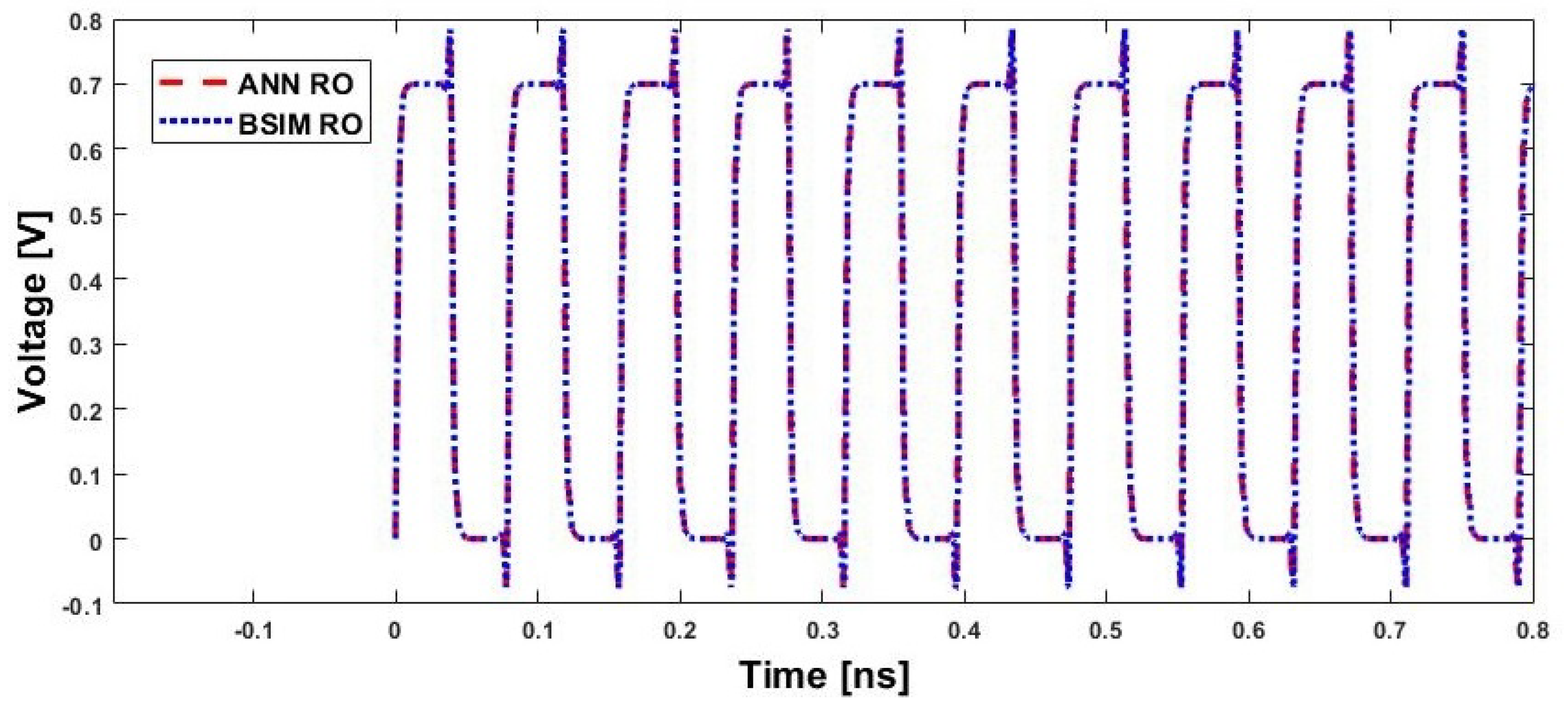
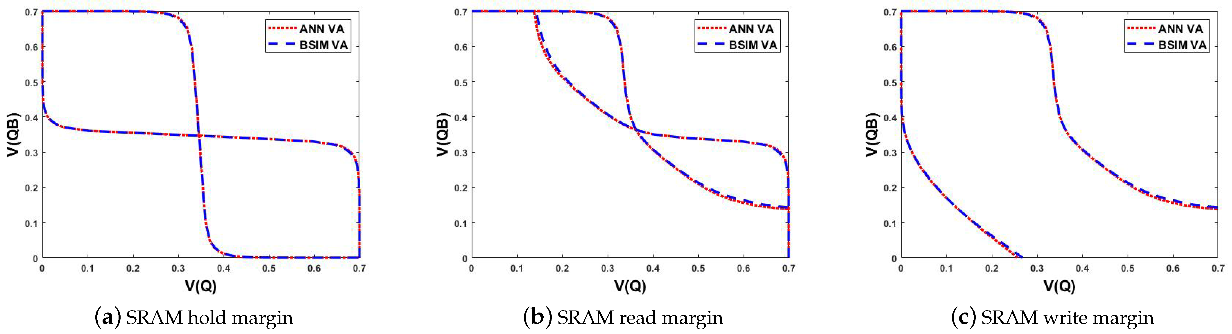
5.1. XOR, Ring Oscillator, and SRAM Simulation
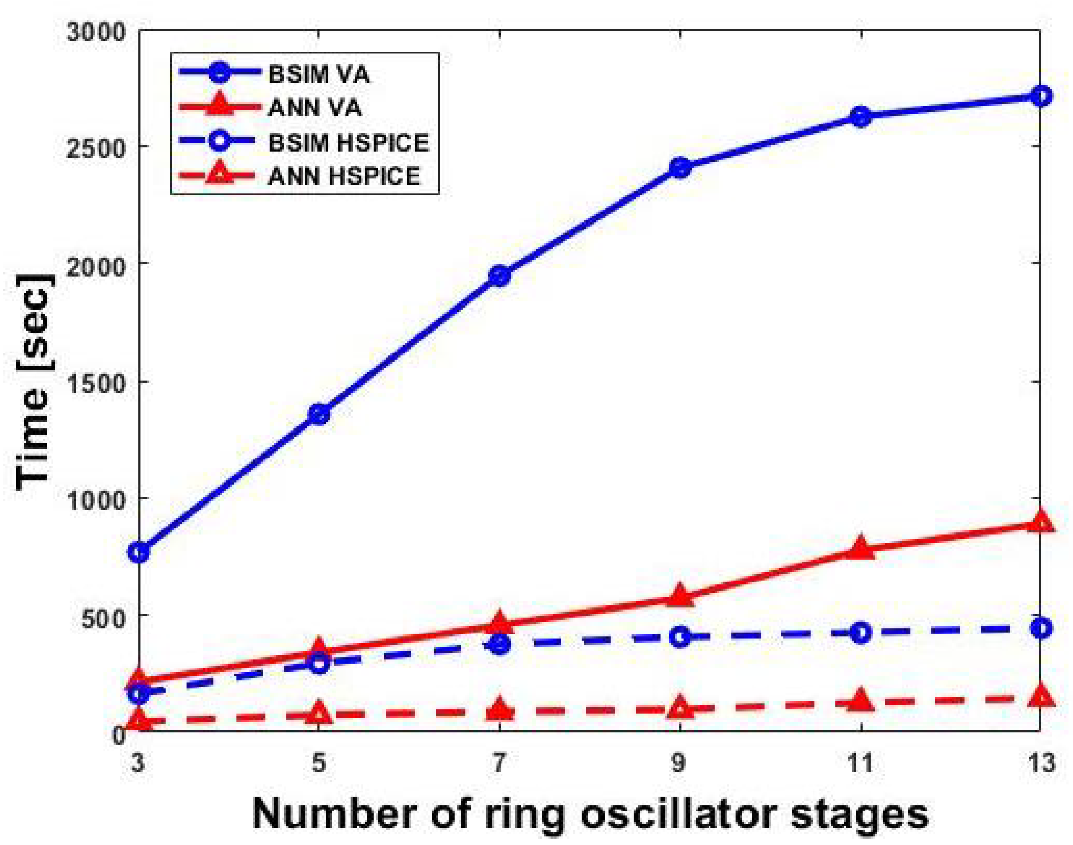
5.2. SPICE Simulation Performance Comparison
5.2.1. Global Device Model
5.2.2. Single-Device Model
6. Conclusions
Author Contributions
Funding
Acknowledgments
Conflicts of Interest
References
- Root, D.E. Future Device Modeling Trends. IEEE Microw. Mag. 2012, 13, 45–59. [Google Scholar] [CrossRef]
- Dunga, M.V.; Lin, C.-H.; Niknejad, A.M.; Hu, C. BSIM-CMG: A Compact Model for Multi-Gate Transistors. In FinFETs and Other Multi-Gate Transistors; Springer: Berlin/Heidelberg, Germany, 2008; pp. 113–153. [Google Scholar]
- Klemme, F.; Prinz, J.; Santen, V.M.V.; Henkel, J.; Amrouch, H. Modeling Emerging Technologies Using Machine Learning: Challenges and Opportunities. In Proceedings of the 2020 International Conference on Computer-Aided Design, New York, NY, USA, 2–5 November 2020. [Google Scholar]
- Lim, J.H.; Shin, C.H. Machine Learning (ML)-Based Model to Characterize the Line Edge Roughness (LER)-Induced Random Variation in FinFET. IEEE Access 2020, 8, 158237–158242. [Google Scholar] [CrossRef]
- Chen, Q.; Chen, G. Artificial Neural Network Compact Model for TFTs. In Proceedings of the 2016 International Conference on Computer Aided Design for Thin-Film Transistor Technologies, Beijing, China, 26–28 October 2016. [Google Scholar]
- Ko, K.; Lee, J.K.; Kang, M.G.; Jeon, J.W.; Shin, H.C. Prediction of Process Variation Effect for Ultrascaled GAA Vertical FET Devices Using a Machine Learning Approach. IEEE Trans. Electron Devices 2019, 66, 4474–4477. [Google Scholar] [CrossRef]
- Lei, Y.; Huo, X.; Yan, B. Deep Neural Network for Device Modeling. In Proceedings of the 2018 IEEE Electron Devices Technology and Manufacturing Conference, Kobe, Japan, 13–16 March 2018. [Google Scholar]
- Zhang, L.; Chan, M. Artificial Neural Network Design for Compact Modeling of Generic Transistors. J. Comput. Electron. 2017, 16, 825–832. [Google Scholar] [CrossRef]
- Zhang, Z.; Wang, R.; Chen, C.; Huang, Q.; Wang, Y.; Hu, C.; Wu, D.; Wang, J.; Huang, R. New-Generation Design-Technology Co-Optimization (DTCO): Machine-Learning Assisted Modeling Framework. In Proceedings of the 2019 Silicon Nanoelectronics Workshop, Kyoto, Japan, 9–10 June 2019. [Google Scholar]
- Mehta, K.; Wong, H. Prediction of FinFET Current-Voltage and Capacitance-Voltage Curves Using Machine Learning with Autoencoder. IEEE Electron Device Lett. 2021, 42, 136–139. [Google Scholar] [CrossRef]
- Wang, J.; Kim, Y.H.; Ryu, J.S.; Jeong, C.W.; Choi, W.S.; Kim, D.S. Artificial Neural Network-Based Compact Modeling Methodology for Advanced Transistors. IEEE Trans. Electron Devices 2021, 68, 1318–1325. [Google Scholar] [CrossRef]
- Hirtz, T.; Huurman, S.; Tian, H.; Yang, Y.; Ren, T.-L. Framework for TCAD augmented machine learning on multi-I-V characteristics using convolutional neural network and multiprocessing. J. Semicond. 2021, 42, 124101. [Google Scholar] [CrossRef]
- Shirakawa, K.; Shimiz, M.; Okubo, N.; Daido, Y. A Large-Signal Characterization of an HEMT Using a Multilayered Neural Network. IEEE Trans. Microw. Theory Tech. 1997, 45, 1630–1633. [Google Scholar] [CrossRef]
- Yoo, S.; Kim, S. Leakage Optimization of the Buried Oxide Substrate of Nanosheet Field-Effect Transistors. IEEE Trans. Electron Devices 2022, 69, 4109–4114. [Google Scholar] [CrossRef]
- Kim, S.-D.; Guillorn, M.; Lauer, I.; Oldiges, P.; Hook, T.; Na, M.-H. Performance Trade-offs in FinFET and Gate-All-Around Device Architecture for 7nm-node and Beyond. In Proceedings of the 2015 SOI-3D-Subthreshold Microelectronics Technology Unified Conference, Rohnert Park, CA, USA, 5–8 October 2015. [Google Scholar]
- Synopsys Inc. Sentaurus Device, User Manual, Version Y-2019; Synopsys Inc.: Mountain View, CA, USA, 2019. [Google Scholar]
- Yoon, J.-S.; Jeong, J.; Lee, S.; Baek, R.-H. Optimization of nanosheet number and width of multi-stacked nanosheet FETs for sub-7-nm node system on chip applications. Jpn. J. Appl. Phys. 2019, 58, SBBA12. [Google Scholar] [CrossRef]
- Ryu, D.; Kim, M.; Yu, J.; Kim, S.; Lee, J.-H.; Park, B.-G. Investigation of Sidewall High-k Interfacial Layer Effect in Gata-All-Around Structure. IEEE Trans. Electron Devices 2020, 67, 1859–1863. [Google Scholar] [CrossRef]
- Yoon, J.-S.; Jeong, J.; Lee, S.; Baek, R.-H. Systematic DC/AC Performance Benchmarking of Sub-7-nm Node FinFETs and Nanosheet FETs. IEEE J. Electron Devices Soc. 2018, 6, 942–947. [Google Scholar] [CrossRef]
- Sun, Y.; Thompson, E.; Nishida, T. Physics of strain effect in semiconductors and metal-oxide-semiconductor field-effect transistors. J. Appl. Phys. 2007, 101, 104503. [Google Scholar] [CrossRef]
- Reboh, S.; Coquand, R.; Augendre, E.; Barraud, S.; Maitrejean, S.; Viner, M.; Faynot, O.; Loubet, N.; Guillorn, M.; Fetterolf, S.; et al. An analysis of stress evolution in stacked GAA transistors. In Proceedings of the IEEE Slilcon Nanoelectronics Workshop (SNW), Honolulu, HI, USA, 12–13 June 2016. [Google Scholar]
- Loubet, N.; Hook, T.; Montanini, P.; Yeung, C.-W.; Kanakasabapathy, S.; Guillom, M.; Yamashita, T.; Zhang, J.; Miao, X.; Wang, J.; et al. Stacked nanosheet gate-all-around transistor to enable scaling beyond FinFET. In Proceedings of the 2017 IEEE Symposium on VLSI Technology, Kyoto, Japan, 5–8 June 2017. [Google Scholar]
- Moore, M. International Roadmap for Devices and Systems (IRDS™) Edition. IEEE. 2021. Available online: https://irds.ieee.org/images/files/pdf/2021/2021IRDS_MM.pdf (accessed on 25 August 2022).
- Paszke, A.; Gross, S.; Massa, F.; Lerer, A.; Bradbury, J.; Chanan, G.; Killeen, T.; Lin, Z.; Gimelshein, N.; Antiga, L.; et al. PyTorch: An Imperative Style, High-Performance Deep Learning Library. In Proceedings of the Advances in Neural Information Processing Systems, Vancouver, BC, Canada, 8–14 December 2019; pp. 8024–8035. [Google Scholar]
- Mcandrew, C.C.; Coram, G.J.; Gullapalli, K.K.; Jones, J.R.; Nagel, L.W.; Roy, A.S.; Roychowdhury, J.; Scholten, A.J.; Smit, G.D.J.; Wang, X.; et al. Best Practices for Compact Modeling in Verilog-A. IEEE J. Electron Devices Soc. 2015, 3, 383–396. [Google Scholar] [CrossRef]
- Lim, W.; Chin, H.C.; Lim, C.S.; Tan, M.L.P. Performance Evaluation of 14nm FinFET-Based 6T SRAM Cell Functionality for DC and Transient Circuit Analysis. J. Nanomater. 2014, 2014, 105. [Google Scholar] [CrossRef]
- Song, T.; Jung, H.; Yang, G.; Tang, H.; Kim, H.; Seo, D.; Kim, H.; Rim, W.; Baek, S.; Baeck, S.; et al. 3nm Gate-All-Around (GAA) Design-Technology Co-Optimization (DTCO) for succeeding PPA by Technology. In Proceedings of the Custom Integrated Circuits Conference (CICC), Newport Beach, CA, USA, 24–27 April 2022. [Google Scholar]
- Kao, M.Y.; Kam, H.; Hu, C. Deep-Learning-Assisted Physics-Driven MOSFET Current-Voltage Modeling. IEEE Electron Device Lett. 2022, 43, 974–977. [Google Scholar] [CrossRef]


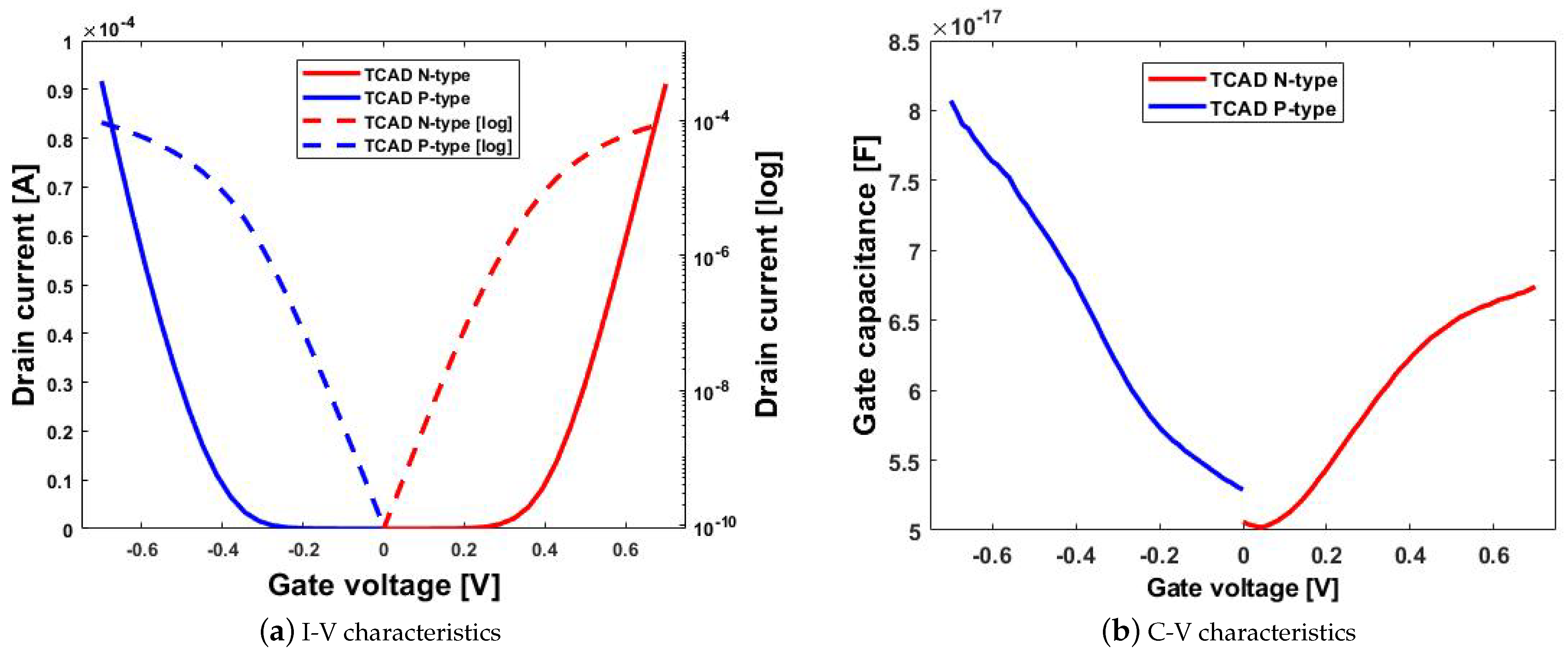
| N-Type NSFET | P-Type NSFET | |
|---|---|---|
| [mV] | 0.218 | 0.220 |
| [pA] | 98.01 | 95.03 |
| [uA] | 91.13 | 90.34 |
| SS 1 [mV/dec] | 65.8 | 66.4 |
| Tech Node | 3 [nm] | 2.1 [nm] | 1.5 [nm] | 3 [nm] | Sub-3 [nm] |
|---|---|---|---|---|---|
| IRDS | IBM | Our Datasets | |||
| L [nm] | 16 | 14 | 12 | 12 | 11, 12, 13 |
| W [nm] | 30 | 30 | 30 | 50 | 21, 23, 25, 27, 29 |
| T [nm] | 8 | 7 | 6 | 5 | 4, 5, 6 |
| L [nm] | 6 | 5 | 4 | 5 | 3, 4, 5 |
| T [nm] | 1.4 | 1.37 | 1.37 | 1.5 | 1, 1.5, 2 |
| T [nm] | 10 | 10 | 10 | 10 | 10 |
| S/D doping [cm] | - | - | - | - | 6.5 × 10 |
| Channel doping [cm] | - | - | - | - | 1 × 10 |
| BSIM-CMG | ANN Model | Errors [%] | ||
|---|---|---|---|---|
| XOR | A to Y Delay [ps] | 11.96 | 11.88 | 0.68 |
| B to Y Delay [ps] | 5.94 | 5.87 | 1.13 | |
| 17-RO | Delay [ps] | 79.50 | 78.70 | 1.01 |
| SRAM (Hold) | Margin [mV] | 286.98 | 285.88 | 0.39 |
| SRAM (Read) | Margin [mV] | 129.68 | 126.01 | 2.91 |
| SRAM (Write) | Margin [mV] | 223.16 | 221.72 | 0.65 |
| Single-Device Model | Global Device Model | |||
|---|---|---|---|---|
| ANN model sizes | I-V | C-V | I-V | C-V |
| (numbers of neurons in hidden layers) | (5, 5) | (5) | (20, 15) | (10, 5) |
| Simulation errors | Off region: 2.5% | C: 1.3% | ||
| 0.3% or less | 0.3% or less | (log scale: 0.2%) | C: 1.5% | |
| Medium region: 2.0% | C: 1.5% | |||
| High region: 1.0% | ||||
| I-V: (7 × 5) + (5 × 5) +(5 × 1) = 65 | I-V: (7 × 20) + (20 × 15) + (15 × 1) = 455 | |||
| Simulation complexity 1 | C-V: (7 × 5) + (5 × 3) = 50 | C-V: (7 × 10) + (10 × 3) = 100 | ||
| Activation function (tanh) calculation = 15 | Activation function (tanh) calculation = 50 | |||
| Advantages | 1. Different devices can be simulated By | |||
| 1. The simulation speed is fast | changing the structural parameters of the circuit | |||
| 2. The accuracy is very high | 2. The circuit specifications (e.g., power, delay) can | |||
| be evaluated based on the structural parameters | ||||
| 3. TCAD usage is reduced by predicting | ||||
| values between structures | ||||
Publisher’s Note: MDPI stays neutral with regard to jurisdictional claims in published maps and institutional affiliations. |
© 2022 by the authors. Licensee MDPI, Basel, Switzerland. This article is an open access article distributed under the terms and conditions of the Creative Commons Attribution (CC BY) license (https://creativecommons.org/licenses/by/4.0/).
Share and Cite
Woo, S.; Jeong, H.; Choi, J.; Cho, H.; Kong, J.-T.; Kim, S. Machine-Learning-Based Compact Modeling for Sub-3-nm-Node Emerging Transistors. Electronics 2022, 11, 2761. https://doi.org/10.3390/electronics11172761
Woo S, Jeong H, Choi J, Cho H, Kong J-T, Kim S. Machine-Learning-Based Compact Modeling for Sub-3-nm-Node Emerging Transistors. Electronics. 2022; 11(17):2761. https://doi.org/10.3390/electronics11172761
Chicago/Turabian StyleWoo, SangMin, HyunJoon Jeong, JinYoung Choi, HyungMin Cho, Jeong-Taek Kong, and SoYoung Kim. 2022. "Machine-Learning-Based Compact Modeling for Sub-3-nm-Node Emerging Transistors" Electronics 11, no. 17: 2761. https://doi.org/10.3390/electronics11172761
APA StyleWoo, S., Jeong, H., Choi, J., Cho, H., Kong, J.-T., & Kim, S. (2022). Machine-Learning-Based Compact Modeling for Sub-3-nm-Node Emerging Transistors. Electronics, 11(17), 2761. https://doi.org/10.3390/electronics11172761