Review

Recent Progress in Fabrication and Physical Properties of 2D TMDC-Based Multilayered Vertical Heterostructures

1
College of Materials and Environmental Engineering, Hangzhou Dianzi University, Hangzhou 310018, China
2
School of Sciences, Hangzhou Dianzi University, Hangzhou 310018, China
*
Authors to whom correspondence should be addressed.
Electronics 2022, 11(15), 2401; https://doi.org/10.3390/electronics11152401
Submission received: 23 June 2022 / Revised: 6 July 2022 / Accepted: 27 July 2022 / Published: 1 August 2022
(This article belongs to the Special Issue Two-Dimensional Materials for Nanoelectronics and Optoelectronics)

Abstract

:
Two-dimensional (2D) vertical heterojunctions (HSs), which are usually fabricated by vertically stacking two layers of transition metal dichalcogenide (TMDC), have been intensively researched during the past years. However, it is still an enormous challenge to achieve controllable preparation of the TMDC trilayer or multilayered van der Waals (vdWs) HSs, which have important effects on physical properties and device performance. In this review, we will introduce fundamental features and various fabrication methods of diverse TMDC-based multilayered vdWs HSs. This review focuses on four fabrication methods of TMDC-based multilayered vdWs HSs, such as exfoliation, chemical vapor deposition (CVD), metal-organic chemical vapor deposition (MOCVD), and pulsed laser deposition (PLD). The latest progress in vdWs HS-related novel physical phenomena are summarized, including interlayer excitons, long photocarrier lifetimes, upconversion photoluminescence, and improved photoelectrochemical catalysis. At last, current challenges and prospects in this research field are provided.

1. Introduction

The great success of graphene obtained in 2004 [1] has promoted the development of novel kinds of 2Dlayered materials and their heterostructures (HSs), ascribing to a distinct layered structure, outstanding optical/electrical/transport features, and prominent stability, guaranteeing them potential candidates for high-performance electronics and optoelectronics [2]. A crucial group of layered materials, TMDCs with the formula of (Mo, W, Re)(S, Se, Te)2 have stimulated broad research interests in the past 12 years due to variable electronic characteristics from insulator, semiconductor, to semi-metallic, metallic, indirect-to-direct bandgap transition, and high carrier mobility as thickness thinned to one layer [3,4,5]. Because of these prominent characteristics, 2D TMDCs have shown tremendous application foreground in electronics [6], optoelectronics [7,8], valleytronics [9], and catalysis [10].
However, several major problems still impede the application of a single 2D monolayer TMDC in current optoelectronics. Particularly, the low light absorption efficiency of ultrathin 2D TMDC flakes will limit external quantum efficiency and detectivity of optoelectronics [11]. Meanwhile, the generation of intralayer excitons in single 2D TMDC crystals is not easily manipulated due to its short lifetime [12], restricting the applications in exciton devices. In contrast, vdW HSs, vertically stacked by different TMDCs, can get rid of the constraint of lattice mismatch and have the flexibility and a sharp heterointerface without atomic commensurability originating from dangling bond-free surfaces of 2D TMDCs, occupy a crucial position in fields of spectroscopy, electronics, catalyst, and optoelectronics, deriving from several novel features that differ from individual 2D TMDCs, for example, interlayer excitons [13], photovoltaic effect [14], carrier recombination [15], ultrafast charge transfer [16], etc. After the first fabrication of graphene/h-BN vertical HS in 2010 [17], various techniques, such as mechanical exfoliation [18,19,20], molecular beam epitaxy (MBE) [21,22,23,24], PLD [25,26], MOCVD [27,28], and CVD [11,29,30,31,32], had been utilized to obtain bilayer TMDCs vdW HSs, such as MoS2/WS2 [13,33,34,35,36,37,38], WSe2/MoS2 [39,40], WSe2/MoSe2 [41], ReS2/WS2 [42], MoSe2/WSe2 [43,44,45], p-MoS2/n-MoS2 [46], MoS2/WSe2 [47], PtS2/PtSe2 [48], NbS2/MoS2 [49,50], MoSe2/MoS2 [51], MoTe2/MoS2 [52], MoS2-WS2/WS2 [53], VSe2/MX2 (M: Mo, W; X: S, Se) [54,55], VS2/WSe2 [55], PtSe2/MoSe2 [56], MTe2/WX2 (M = V, Nb, Ta; X = S, Se) [57], WS2/WSe2 (MoSe2) [58], WSe2/WS2 [59,60,61], NiTe2/MoS2 [62], MTe2/WSe2 (M = Ni, Co, Nb, V) [55], VSe2/WSe2 [55], WX2-MoX2/WX2-MoX2 (X = S, Se) [63], WSe2/WS2(1−x)Se2x [64], Mo6Te6/MoS2(1−x)Te2x [65], WSe2/CrSe2 [66], MoSe2/NbSe2 [67], WS2/MoWS2 [11,29,31,32], and so forth. Usually, the physical properties of 2D TMDCs can be modulated by adjusting composition, thickness, stacking order, and angle. As a consequence, plenty of research enthusiasm has been contributed to the construction and exploration of the attractive characteristics of trilayer or multilayered TMDC vdW HSs, as shown in Figure 1, which presents enhanced light absorption ranging from the UV to NIR light region [68] and long recombination lifetimes of interlayer excitons (~100 ns) [69,70]. New fabrication approaches for the design and production of TMDC-based multilayered HSs are still at their primary stage, and to date, diverse methods have been utilized and verified. More developments are still needed to further figure out the effect of various preparation methods on the final properties of as-produced materials.
Here, we summarize the recent progress in the preparation of diverse 2D TMDC multilayered vdW HSs. In particular, we mainly concluded the latest progress in the preparation of 2D TMDC multilayered vdW HSs via four growth strategies, such as the exfoliation method, CVD, MOCVD, and PLD. These advances in fabrication strategies have realized the preparation of diverse 2D TMDC vdW HSs with fascinating characteristics, including tunable interlayer excitons, long carrier lifetime, upconversion light emission, etc., which ensure the promising applications in future optoelectronics. Finally, a summary and perspectives of further investigations in the multilayer heterostructure fabrication will also be discussed.

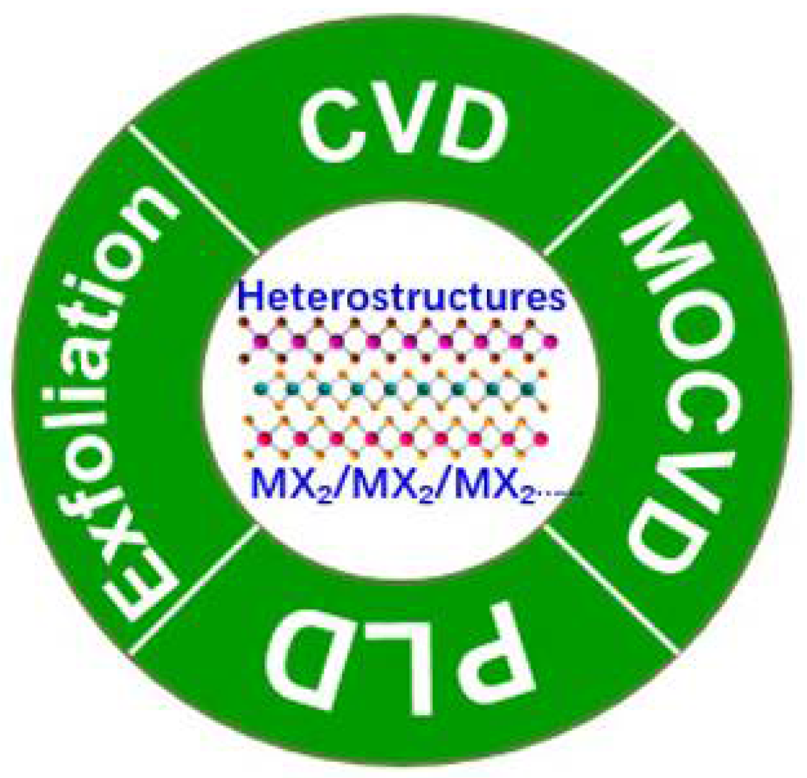
2. Fabrication Methods of 2D TMDC-Based Multilayered vdWs HSs

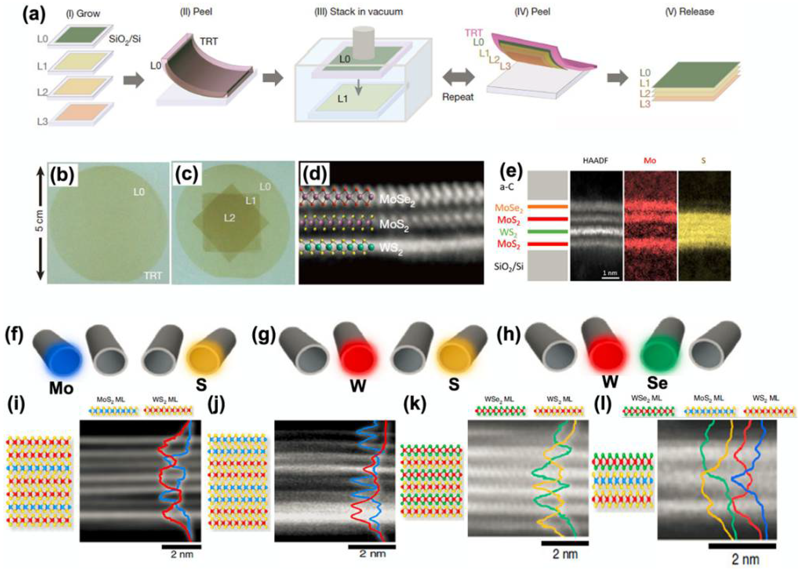
2.1. Exfoliation Method

The exfoliation method is a typical top-down method, which basically involves peeling off a single or several layers of 2D crystals from bulk TMDCs. Such procedures can not only be carried out in the air via mechanical exfoliation but also can be performed chemically or electrochemically in solution, defined as chemical or electrochemical exfoliation.
Recently, the mechanical exfoliation method was widely applied to construct the 2D TMDC-based multilayered vdW HSs [71,72,73,74,75,76,77,78,79,80,81,82,83]. Surrente et al. achieved the fabrication of MoS2/MoSe2/MoS2 vdW HSs, as drawn in Figure 2a, via two-step wet transfer [84]. First, the upper-MoS2 monolayer was transferred to a CVD-synthesized MoSe2 monolayer. Whereafter, the bilayer MoS2/MoSe2 vdW HS was transferred to a CVD-synthesized bottom MoS2 monolayer; the corresponding typical optical microscope (OM) image of the final product of the MoS2/MoSe2/MoS2 trilayer vdW HSs is provided in Figure 2b. Furthermore, Ceballos et al. elucidated the construction of a trilayer WSe2/MoSe2/WS2 and a four-layer WSe2/MoSe2/WS2/MoS2 vdW HSs via a multi-step exfoliation and transfer approach, and corresponding OM images of these products are provided in Figure 2c,d [74]. Typically, the single-layer WSe2, MoSe2, WS2, and MoS2 crystals were first mechanically exfoliated from bulk counterparts utilizing adhesive tape. Many crystals on the tape were then transferred onto a flexible PDMS. After the single-layer flakes were transferred onto a rigid substrate (quartz or Si substrate), the samples were then thermally treated at low pressure (~2–3 Torr) and 200 °C for 2 h under a mixed gas of H2(20 sccm)/Ar (100 sccm). For multilayered HSs, after the annealing procedure, the above-mentioned process was repeated until a product with a desired stacking vdW HS was produced. Moreover, large-scale 2D TMDC-based vdW HSs can also be achieved using the exfoliation approach. For example, Boandoh et al. demonstrated the preparation of wafer-scale vdWs HSs via the aid of viscoelastic polymer, and the corresponding schematic diagram of the fabrication of wafer-scale MoS2/WS2/MoSe2/WSe2 vdWs HSs is depicted in Figure 2e [75]. During the preparation, the viscoelastic polymer-supported layer (VEPSL) was firstly spin-coated onto the topmost layer of an as-grown 2D flake for assembly, followed by annealing (90 °C) above Tg to prompt conformal contact between VEPSL and 2D material. The VEPSL/2D film is detached from the growth substrate and dried. Such resulted film is then stacked onto the next 2D layer. Attaching and detaching after annealing are repeated to construct the desired stacked vdW HSs. Ultimately, VEPSL is removed under proper conditions, and the typical schematic and OM image of the as-prepared wafer-scale MoS2/WS2/MoSe2/WSe2 vdWs HS are provided in Figure 2f. Meanwhile, Han et al. exploited a feasible strategy for manufacturing wafer-scale 2D TMDC layers of certain composition and crystal orientation on PET [78]. The first step of this method is to attain the scalable CVD preparation of 2D TMDC layers on “water-dissoluble” salt wafers, which can be recycled for follow-up growth. Second, the obtained TMDC products are put in deionized water until complete delamination and then transferred to fresh deionized water to remove residual salts. Two-dimensional TMDC layers integrated on secondary substrates are dried to eliminate residual water. Finally, the setup and loading rod can realize the automated integration of MoS2/PtSe2/PtTe2 HSs on a PET substrate, and the detailed preparation process and typical OM image of as-produced MoS2/PtSe2/PtTe2 HSs are shown in Figure 2g,h. In addition, Bae et al. reported the preparation of a WSe2/MoTe2 heterobilayer and WSe2/MoTe2/WSe2 heterotrilayer via mechanical exfoliation; the related OM image and band alignment are shown in Figure 2i [83]. Typically, single-layer WSe2 and MoTe2 are mechanically exfoliated from the bulk crystals, and they are stacked utilizing a dry-transfer strategy on a Si/SiO2 (300 nm) substrate. It can be noted that the thin BN layers are placed at the upper- and bottom-position of such as-produced vdW HSs, which were employed to encapsulate the top and bottom of the HSs, protecting the products from possible unwanted contamination during the experiments.

2.2. Chemical Vapor Deposition (CVD)

CVD is a vapor-phase growth technique and is widely employed to grow low-dimensional nanostructures, which essentially includes vaporization and dissociation of precursors, vapor transportation, and chemical reactions so as to synthesize desired solid compounds. For a typical CVD process, diverse growth factors can be tuned to modulate the growth. For instance, types of precursors can determine the phase and stoichiometry of resulting samples; vaporization temperature can mainly affect the volatility and saturated vapor pressure of source materials; the pressure of the CVD system can modulate volatilization and vapor pressure of precursors; the kind, size, and amount of catalysts can affect the size and shape of final products. In addition, the substrate temperature, as well as gas flow rate, growth time, and type of deposition substrate, will strongly influence the as-grown product [84]. In consequence, rational selection and modulation of growth factors during CVD growth can facilitate the design and construction of numerous processes and pathways to achieve controllability. In the following, we will represent some of the currently developed CVD techniques for the fabrication of 2D TMDC-based multilayered vdW HSs.
During the multi-step CVD procedure, sequential growth of various 2D TMDC layers will facilitate the formation of 2D TMDC multilayered vdW HSs by adjusting growth temperature. For example, Lin et al. illustrated the formation of MoS2/WSe2/graphene(M/W/G) and WSe2/MoS2/graphene(W/M/G) vdWs HSs [39]. In this work, graphene on a 6H-SiC substrate via the CVD method is utilized as the growth substrate for the two-step CVD fabrication of M/W/G and W/M/G vdWs HSs via changing the growth temperature and precursors, as depicted in Figure 3a. Typically, the growth temperature of the WSe2 layer is 950 °C, while the growth temperature of the MoS2 layer is 750 °C, inducing the formation of vdWs HSs with opposite stacking sequences by manipulating the growth temperature at different CVD growth steps. The TEM images of the vdWs HSs displayed in Figure 3b,c demonstrated the successful growth of M/W/G and W/M/G vdWs HSs. Currently, Li et al. realized the first fabrication of lots of multilayered(m)/single-layer(s) TMDCs vdWs HS arrays with varied edge sizes at predesignated locations, including (V, Ni, Co, Nb)Se2/WSe2, VS2/WSe2, and VSe2/(Mo, W)S2 [55]. Figure 3d describes the controlled nucleation and formation of m-VSe2 on large-size WSe2 film. Typically, WSe2 film with several layers was firstly fabricated in reverse-flow CVD equipment, which can not only reduce the nucleation density during the heating stage, but also ensure high quality of the underlying WSe2 film with large size and few defects. Whereafter, laser cauterization was performed on as-grown WSe2 film, resulting in the creation of a periodically aligned defect array. At last, the preparation of few-layer VSe2 at the top of the pre-grown film was implemented in a two-zone furnace. By selecting an appropriate reaction temperature and growth time for the upper VSe2 film, obtained VSe2/WSe2 HS arrays present a high crystalline quality with distinguishable WSe2 and VSe2 parts with pink and yellow color as well as distinct boundaries between them; OM image is shown in Figure 3e,f. The corresponding HRTEM characterization in Figure 3g indicates that VSe2 crystals began to grow laterally and resulted in a perfect vdWs interface between one-layer WSe2 and bilayer VSe2 without any lattice distortion. AFM image in Figure 3h further verified the highly uniform characteristic of the HS arrays. The Raman intensity mapping images in Figure 3i,j exhibit evident spatial variation and further elucidate the generation of stacked VSe2/WSe2 HS arrays. Meanwhile, PL intensity mapping in Figure 3k presents analogous characteristics to Raman mapping results, verifying that the optical quality of WSe2 film is largely unaffected during the fabrication of VSe2. Recently, our group realized a one-step CVD synthesis of various bilayer, trilayer, and four-layer TMDC vdW HSs via utilizing Mo (or W) foil, WO3 (or MoO3), and S powder as precursors, as described in Figure 3l [38]. For route 1 (Mo foil and WO3 powder), 1L-MoS2/1L-WS2, 1L-MoS2/2L-WS2, 2L-MoS2/2L-WS2, and 3L-MoS2/1L-WS2 vdWs HSs with WS2 layer at the bottom and MoS2 layer at the top have been fabricated by changing growth temperature from 875 to 950 °C while other growth parameters keep constant, and related OM images are supplied in Figure 3m–p. However, for route 2 (W foil and MoO3 powder), 1L-WS2/1L-MoS2 vdWs HS with the bottom of the MoS2 layer and the top of the WS2 layer at the top, as exhibited in Figure 3q, can be obtained. Corresponding atomic structures of these vdWs HSs are described in Figure 3r. Systematical characterizations indicate that the preparation of various multilayered vdW HSs originated from characteristic differences between metallic foil and oxide powder and the effect of growth temperature on the Mo/W atom ratio and the reaction with S. Moreover, Zhao et al. developed a feasible pathway to obtain vdW superlattices via rolling up vdW HSs [67]. They used SnS2/WSe2 vdW HSs as an example to elucidate the rolling-up process to high-order vdW superlattices. Figure 3s,t displays typical OM images of a triangular flake of monolayer WSe2 after first-step CVD growth and a bilayer SnS2/WSe2 vdW HS after second-step growth. The uniform optical contrast of the SnS2/WSe2 vertical heterobilayer (Figure 3t) indicates that the WSe2 monolayer is completely covered by the SnS2 monolayer, generating a material foundation for the preparation of roll-up vdW superlattices. Using ethanol-water-ammonia solution, SnS2/WSe2 vdW HSs spontaneously roll up to create SnS2/WSe2 roll-ups, as exhibited in the OM image (Figure 3u) and SEM image (Figure 3v). As shown in Figure 3w, the STEM image further displays roll-up structure, with SnS2 and WSe2 layers in SnS2/WSe2 vdW HSs. The higher-resolution STEM image in Figure 3x reveals the atomically resolved SnS2/WSe2 vdW superlattice structure, which comprises alternating layers of monolayer WSe2 and monolayer SnS2, as verified by EDS characterization. Meanwhile, such an approach can be extended to include 3D bulk thin-film materials or 1D nanowires to generate mixed-dimensional vdW superlattices, such as 3D/2D (Al2O3/WSe2), 3D/2D/2D (Al2O3/SnS2/WSe2), 1D/2D (Ag nanowire/WSe2), and 1D/3D/2D (Ag nanowire/Al2O3/WSe2) vdW superlattices, as shown in Figure 3y,z.

2.3. Metal-Organic Chemical Vapor Deposition (MOCVD)

According to early commercial applications in III–V (or II–VI) semiconductors, MOCVD is a promising technique for the preparation of wafer-scale and high-quality electronic and optoelectronic materials and their HSs [85]. Such a method has recently been applied to prepare 2D vdW materials for diverse optoelectronic applications [86,87,88,89,90,91,92]. The prominent advantage of MOCVD is that it is readily transportable and employs high-purity organometallic (MO) precursors that benefits the preparation of 2D TMDC crystals [93]. Importantly, abundant 2D TMDC crystals, which are difficult to be grown by employing other methods, can be synthesized utilizing MOCVD, owing to the large driving force for the pyrolysis of source materials.
For example, Kang et al. elucidated the creation of wafer-scale 2D TMDC films with excellent spatial uniformity and perfect interfaces through the MOCVD technique. The composition and properties of the films in a vertical direction can be modulated at an atomic scale by employing layer-by-layer stacking of 2D TMDCs [27]. As described in Figure 4a, the authors developed a programmed vacuum stack (PVS) process, including five steps: (I) wafer-scale 2D TMDC monolayers are synthesized individually via the MOCVD method; (II) initial layer L0 is mechanically peeled from the deposition substrate utilizing a thermal release tape (TRT); (III) L0/TRT is stacked on the L1 layer in a vacuum chamber; (IV) L1/L0/TRT is peeled off the substrate, and then steps (III)–(IV) are repeated until the film possesses desired layer number NL; and (V) NL-layer film is released from TRT onto a target substrate. Figure 4b,c exhibits images of single-layer and three-layer TMDC films obtained from the above-mentioned steps. Figure 4b displays a 5 cm diameter, circular region of L0 (left), and a trilayer TMDC film (Figure 4c) after two 2.5 cm wide squares of monolayer L1 and L2 are stacked on L0. The layer of L0–L2 still retains continuity and uniformity in Figure 4b,c. STEM image of a MoSe2/MoS2/WS2 film in Figure 4d exhibits that the armchair axes of MoSe2 (top) and MoS2 (middle) are parallel to the electron beam, while that of WS2 is not. Such a result indicates that vertical stacking is viable without the constraints of lattice mismatch and interlayer rotation. Using the above-mentioned approach, MoSe2/MoS2/WS2/MoS2 can also be fabricated, and the corresponding ADF STEM and EELS mapping for Mo and S signals of the HS are supplied in Figure 4e, elucidating the formation of MoSe2/MoS2/WS2/MoS2 HS.
It is well known that the precise integration of each kind into vdWs superlattices (SLs) could enable the realization of special structures with unexplored functionalities. In this regard, Jin et al. demonstrated the layer-by-layer epitaxial growth of TMDC-based vdW SLs with programmable stacking periodicities, which consisted of more than two kinds of dissimilar TMDC MLs, such as MoS2, WS2, and WSe2 [28]. In this work, elemental change in MX2 SLs can be realized either in M-alteration (MX2/M’X2) or X-alteration (MX2/MX’2) with time-lapse precursor variations via MOCVD, as drawn in Figure 4f–h. During MOCVD preparation using the Mo(CO)6 and W(CO)6 precursors, the first bottom MoS2 ML for all SLs was generated by multiple nucleations on regular step and terrace terrains of c-sapphire to trigger preferential in-plane crystal orientations. To accelerate the subsequent ML-by-ML epitaxy, first, bottom ML templates were mechanically transferred onto SiO2/Si substrate. However, direct successive SL growth on the sapphire substrate without the transfer of the first MLs often leads to undesirable local overgrowth due to the special surface structure of c-sapphire, which can provide additional nucleation sites for second MLs other than homogeneous nucleation on the first bottom layer. By kinetics-controlled growth in the near-equilibrium limit via MOCVD, diverse SLs, including MoS2/WS2 SLs with 1:2 periodicity (7 ML stacks) (i), MoS2/WS2 SLs with 2:2 periodicity (8 ML stacks) (j), WSe2/WS2 SLs (6 ML stacks) (k), and WSe2/MoS2/WS2 trilayers (l), can be obtained, as HAADF-STEM images with EDX spectra (right) shown in Figure 4i–l.

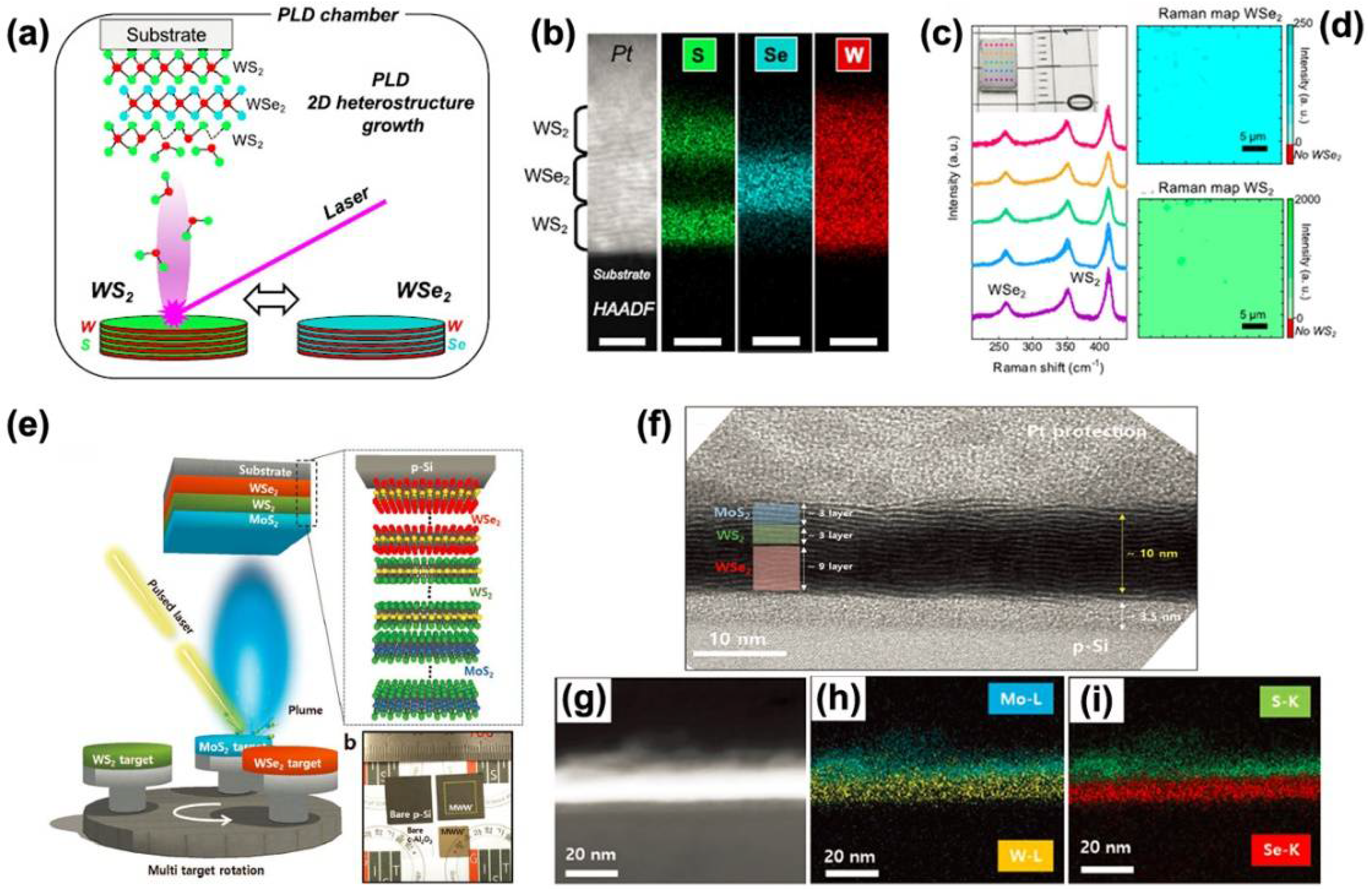
2.4. Pulsed-Laser Deposition (PLD)

Recently, researchers have been developing pulsed-laser deposition (PLD) for the fabrication of 2D TMDC materials. Particularly, PLD has tremendous potential to attain the realization of large-scale and high-quality 2D TMDC materials attributing to several reasons: (i) PLD is feasible and precursor-free, resulting in high efficiency and low contamination; (ii) pulsed lasers with high energy induce a resulting plume with high activity that decomposes almost all condensed matter, facilitating the formation of large-scale 2D TMDCs crystals; (iv) bombarded energetic atoms benefit for reducing growth temperature [94]. Consequently, the direct fabrication of 2D TMDC materials on polymer substrates, which are unstable at high temperatures, is practicable. For example, Zatko et al. developed a strategy to construct functional 2D TMDC vdWs HSs utilizing PLD [25]. In this study, WS2/WSe2/WS2 vdWs HS can be fabricated in situ simply by switching WS2 and WSe2 targets during the PLD, as described in Figure 5a. The TEM and EDS results in Figure 5b,c reveal that the produced sample is a well-defined HS of 2D TMDC. As provided in Figure 5b,c, Raman characterizations on both point and area scales further elucidate the high homogeneity of as-produced HS. Furthermore, Seo et al. reported multi-step preparation of WSe2, WS2, and MoS2 utilizing PLD via the in situ changing target, as drawn in Figure 5e [95]. Cross-sectional TEM characterization is conducted to confirm the detailed thickness of WSe2/WS2/MoS2 thin film, and a corresponding cross-sectional TEM image is provided in Figure 5f. The total thickness of WSe2/WS2/MoS2 vdW film was 10 nm, and the thickness of each monolayer TMDC was ≈0.62 – 0.67 Å. However, the same crystalline structure of the three TMDC made it difficult to distinguish each TMDC layer in TEM images, as displayed in Figure 5f. Therefore, EDS mapping was further employed to identify the position of different layers in the HS. As EDS mapping provided in Figure 5h,i, the elements of Mo, W, S, and Se can be well separated.

3. Typical Property Features of 2D TMDC-Based Multilayered vdWs HSs

Two-dimensional TMDC-based multilayered vdWs HSs, constructed by dissimilar 2D materials with different components and electronic properties, provide a rich and robust material platform for fundamental research on condensed matter physics. In this part, we will briefly introduce some novel physical phenomena and unique properties that emerged in fabricated 2D vdWs HSs to verify their importance and potential.

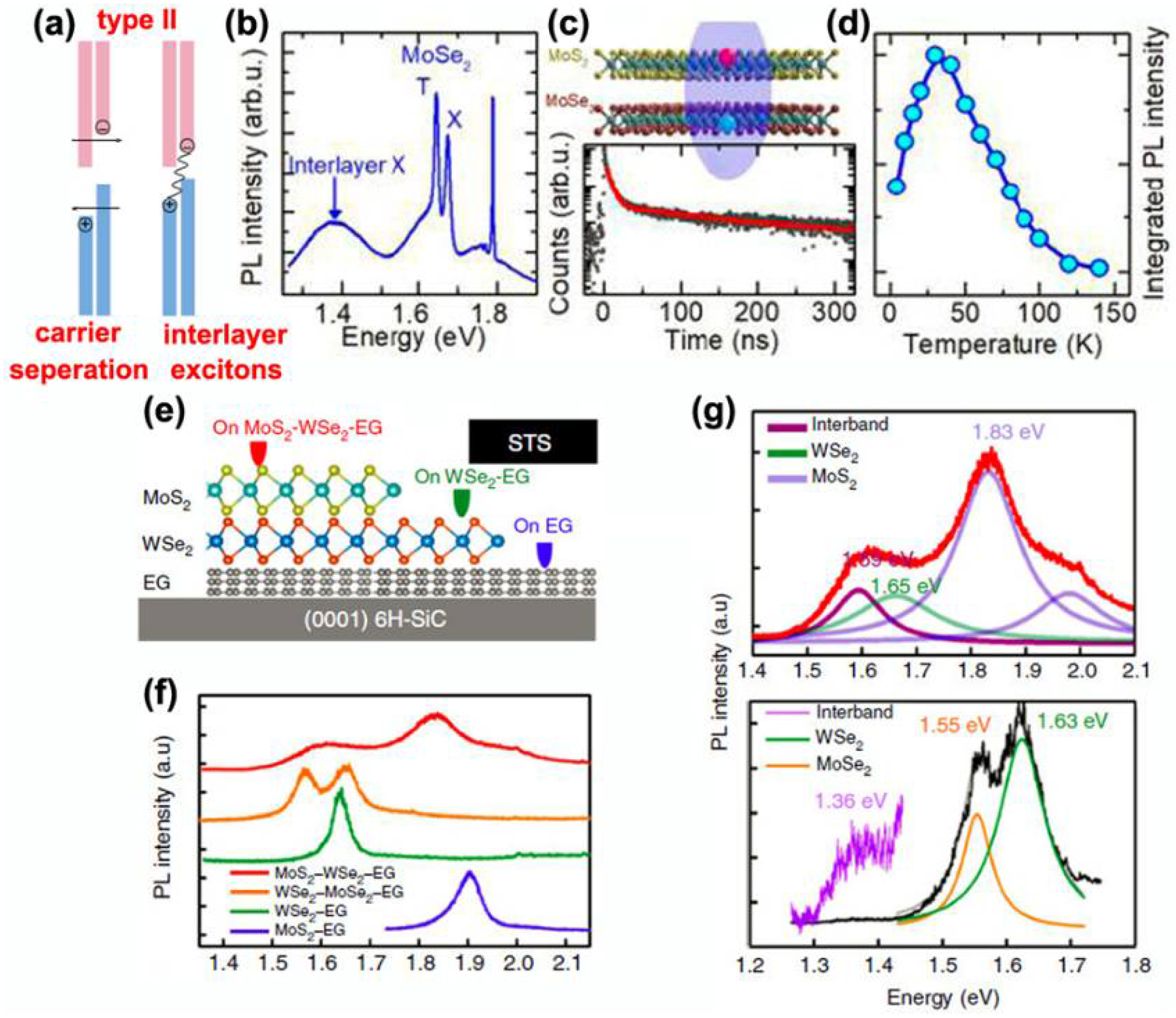
3.1. The Generation of Interlayer Excitons

The creation of s-TMDC/s-TMDC vdWs HSs has emphasized the importance of interlayer coupling, offering an opportunity to pursue the fundamental physics of interlayer excitons (IXs) [96]. For type II HSs, photoexcited electrons from conduction band minimum (CBM) and holes from valence band maximum (VBM) can be rapidly relaxed and localized in the band edges of two dissimilar layers, as illustrated in Figure 6a [97]. Such Coulomb-bound electron-hole pairs formed in vdWs HSs are defined as IXs, whose characteristic is the existence of a new PL peak with lower energy. For example, Baranowski et al. elucidated the long-lived interlayer exciton emission from trilayer MoS2/MoSe2/MoS2 vdWs HS, which is produced via the combined approach of CVD and transfer [69]. Figure 6b shows the typical PL spectra (T = 10 K) of trilayer MoS2/MoSe2/MoS2 vdWs HS. Such PL spectrum of the vdWs HS is dominated by a broad, bound exciton emission, nature of CVD-grown TMDCs. Two emission peaks located in the range of 1.6~1.8 eV can be ascribed to neutral and charged free excitons from MoSe2. However, a relatively weak peak at 1.38 eV can be distinguished in the trilayer HS. The remarkable improvement of the optical quality of the MoSe2 layer realized in the trilayer vdWs HS allows the appearance of a relatively weak peak at 1.38 eV, much lower than the trion and exciton lines of MoSe2. It is well known that trion is charged excitons, including negatively and positively charged excitons, and bound states of two electrons (holes) to a hole (electron) induce the formation of negatively (positively) charged excitons. Such a low energy emission only appeared in the HS region, and its existence is accompanied by a remarkable intensity reduction of the PL spectra corresponding to intralayer excitons in MoS2 or MoSe2. However, such a low energy peak did not appear in MoS2 or MoSe2 monolayers, and a defect-related origin is unlikely. In this regard, a weak peak at 1.38 eV can be attributed to the recombination of an interlayer exciton from the MoSe2 layer and MoS2 layer. Figure 6c depicts time-resolved PL spectra of the HS, and the PL decay is characterized by two-time scales, which can be extracted using a bi-exponential fit (red line), giving decay times ≈5 and ≈135 ns for the fast and slow components of the decay at T = 6 K. Figure 6d depicts the temperature-dependent integrated PL intensity of the interlayer exciton at 1.38 eV. The intensity evolution of the IX transition as a function of measured temperature can conclude that an increase of PL intensity with temperature originated from increasing efficiency of indirect transition with the increasing population of phonons, and the decreasing intensity at higher temperature is attributed to thermal activation of nonradiative recombination channels. Meanwhile, Lin et al. verified the construction of MoS2/WSe2/graphene(M/W/G) and WSe2/MoS2/graphene(W/M/G) vdWs HSs and studied the coupling in the HSs [39]. PL spectra of the different locations from the two HSs, as drawn in Figure 6e, are measured and described in Figure 6f,g. Generally, single-layer semiconductor TMDCs display a direct optical bandgap (Eopt) (MoS2 at 1.8~1.9 eV, MoSe2 at 1.55 eV, and WSe2 at 1.6~1.65 eV). As shown in Figure 6f,g, PL spectra evidence the electronic coupling between the layers. Suc PL spectra not only include the typical peaks from direct bandgap within individual layers but also confirm the presence of interlayer excitons at 1.59 eV for M/W/G and 1.36 eV for W/M/G from the HS region. Therefore, MoS2/WSe2 and WSe2/MoS2 junctions present type-II band alignment.

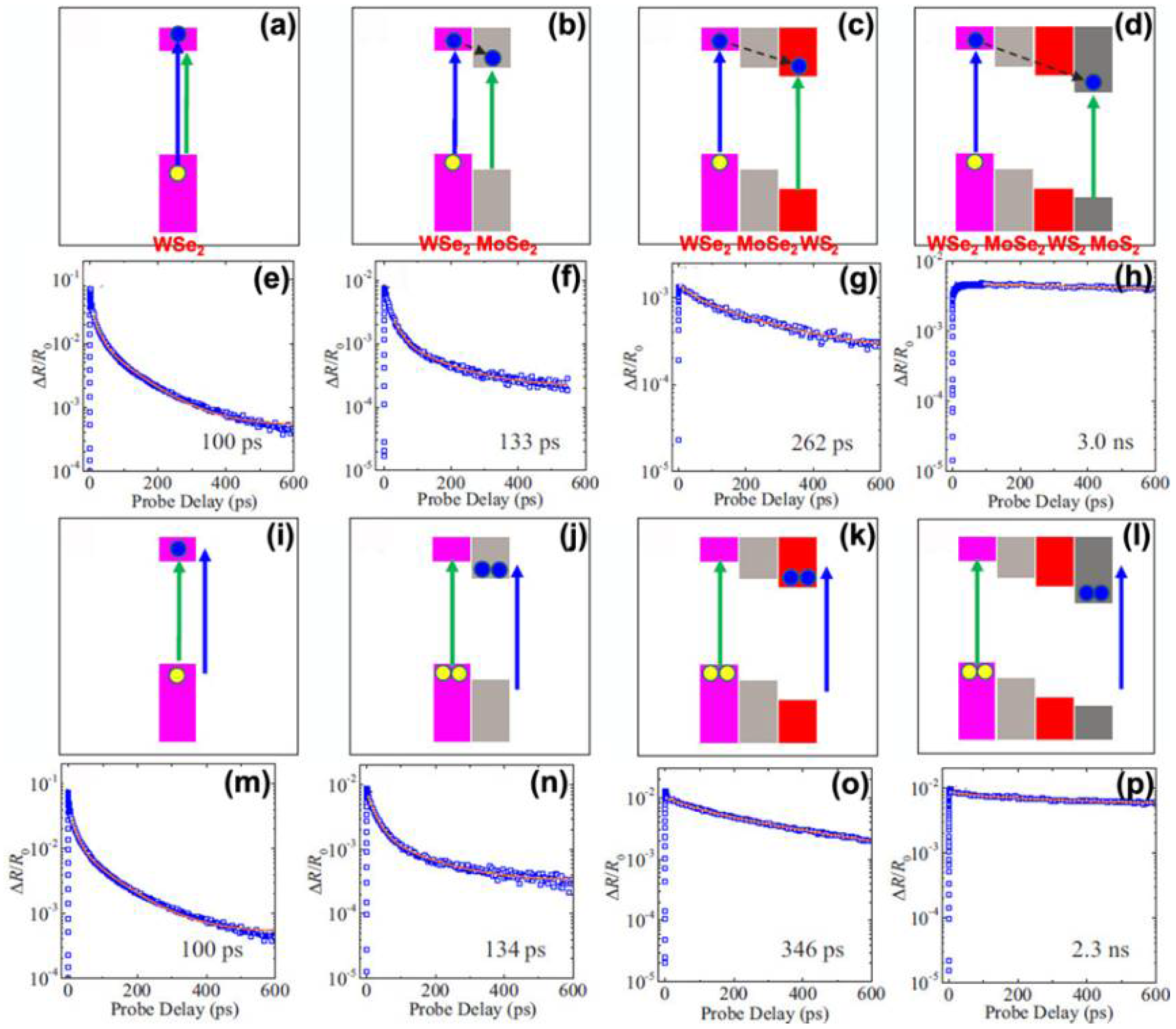
3.2. Long Photocarrier Lifetimes

The heterogeneous integration of TMDC layers with dissimilar compositions guarantees flexible construction of vdWHs with desired band alignments and electronic structures, offering an ideal platform for optoelectronic devices. Especially, multilayered vdW HS-based photodetectors can take full advantage of the characteristics of different components to address some significant challenges encountered by monocomponent devices, such as low light absorption and too-short photocarrier lifetimes. Accordingly, Ceballos et al. realized the fabrication of monolayer WSe2, bilayer WSe2/MoSe2 HS, trilayer WSe2/MoSe2/WS2 HS, and four-layer WSe2/MoSe2/WS2/MoS2 HS, and studied the absorbance and photocarrier lifetimes [74]. Figure 7a–d draws the pump-probe configurations and projected electron transfer in the four samples. Blue and green arrows represent the energies of the pump and probe photons. Such measurements can measure the electron dynamics in the four samples. For each sample, measurements were performed with different values of pump flux and hence different injected carrier densities. As the differential reflection of the 790 nm probe in the long time scale shown in Figure 7e–h, the electron lifetime presents a sharp increase from 100 ps to 3.0 ns, as the sample varies from 1L-WSe2 to four-layer WSe2-MoSe2-WS2-MoS2. Notably, the electron lifetime in the 4L sample is extended several hundred times longer than that in the 1L sample. Meanwhile, the authors also measured the hole dynamics in the four samples by utilizing pump-probe configurations drawn in Figure 7i–l, and corresponding results are provided in Figure 7m–p. From measurements in long time ranges, as present in Figure 7n–p, the hole lifetimes are 134 ps, 346 ps, and 2.3 ns in the 2L, 3L, and 4L samples, respectively, which are reasonably consistent with electron lifetimes estimated in the same samples. This study demonstrates that the transfer time of electrons across the multilayer increases from a fraction of picosecond in 2L to about 14 ps in the 4L, while the photocarrier lifetime is extended from about 100 ps to more than 3 ns in the 4L. The modified performance of these TMDC multilayered HSs indicates prospective applications in ultrathin photovoltaic and photodetection devices.

3.3. Upconversion Photoluminescence

Upconversion PL is commonly detected in rare-earth-doped materials and discovered applications in biological imaging, infrared light detection, and laser cooling. Recently, upconversion PL can also be realized in 2D TMDCs via applying strong coupling between charge carriers. For example, Hao et al. realized the fabrication of trilayer MoSe2/WS2/MoS2 vdWs HS via mechanical exfoliation and transfer, as OM image is supplied in Figure 8a, and demonstrated the emergence of upconversion PL in the vdWs HS [76]. For the upconversion PL measurement, by exciting MoSe2 and MoS2 layers with a 670 nm laser, a peak at 620 nm appears. Such upconversion PL can be ascribed to the transfer of electrons and holes from MoSe2 and MoS2, respectively, to the middle layer of WS2, where they recombine, as band alignment described in Figure 8b. Detailed characterizations and analyses of the upconversion PL are provided in Figure 8c–f. As shown in Figure 8c, black squares exhibit PL spectrum from trilayer vdWs HS under excitation laser wavelength of 670 nm with a power of 10 μW, while the 785 nm laser is blocked. The PL has an emission peak of 620 nm, which is ~50 nm shorter than the excitation wavelength. The 670 nm laser is tuned to the optical bandgap of MoS2 but also can excite MoSe2 (optical bandgap of 785 nm). In this regard, the PL peak at 620 nm ascribes to the recombination of excitons generated by electrons from MoSe2 and holes from MoS2 in WS2 because WS2 can not be excited. To confirm this interpretation, the PL measurements are performed at different excitation wavelengths with varied power. The power dependence of upconversion PL spectra is measured and summarized in Figure 8d–f. At first, the authors fixed the power of the 785 nm beam at 10 μW and obtained PL spectra from the HS region with tunable power of 670 nm laser, as plotted in Figure 8d. Red squares in Figure 8f describe the relationship of peak and 670 nm power, which is concluded from Figure 8d, agreeing with the mechanism of upconversion PL depicted in Figure 8b. Whereafter, they fixed 670 nm power and estimated how the PL spectra changed with 785 nm power. As the PL feature shows in Figure 8e and the blue circles in Figure 8f, a changing trend can be ascribed to the 785 nm laser only exciting the MoSe2 layer. The results elucidate an unexplored physical mechanism for upconversion PL in 2D materials and recommend vdWs HSs as materials to achieve upconversion PL.

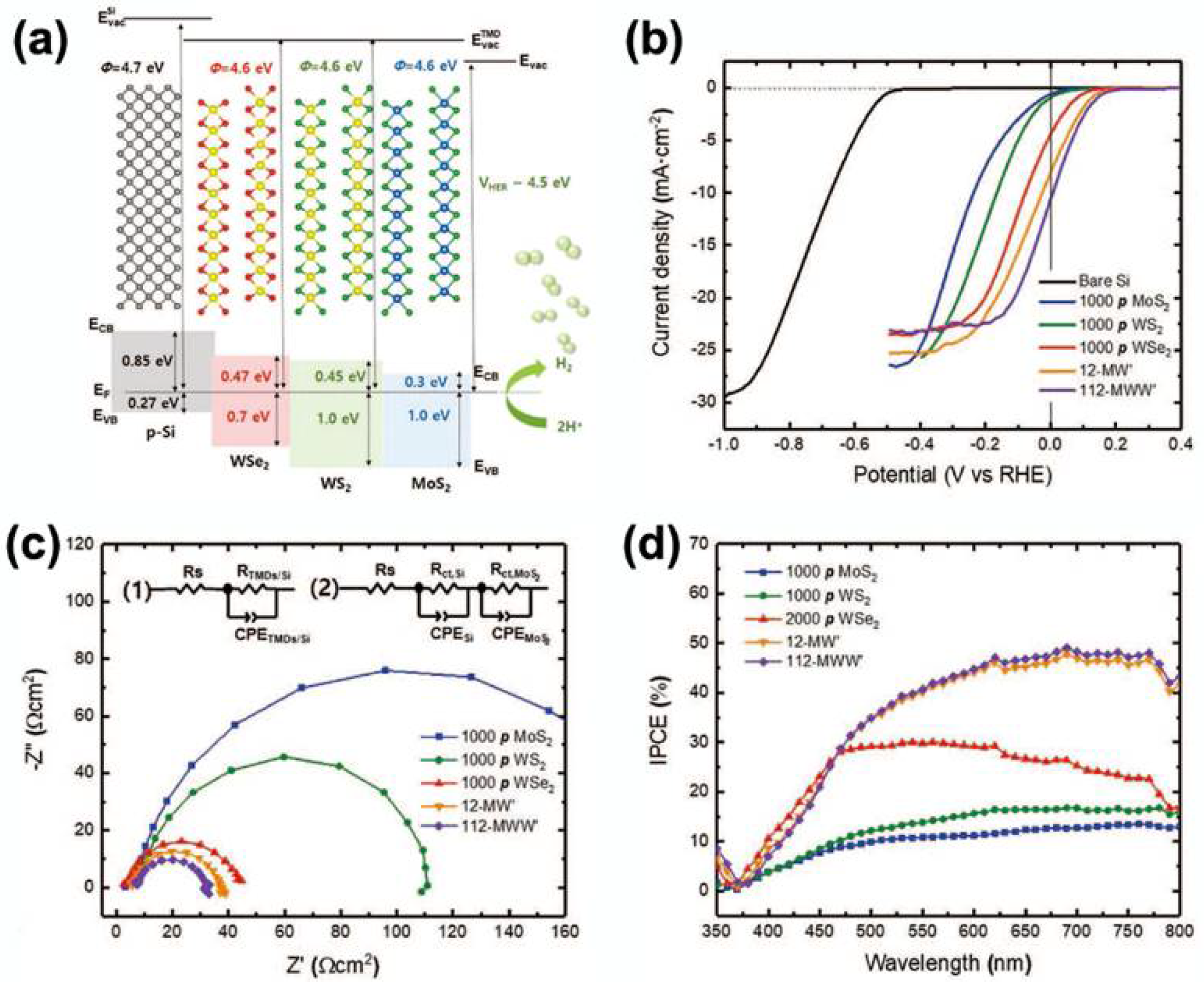
3.4. Improved Photoelectrochemical (PEC) Catalysis

An unprecedented direction for the application of TMDCs-based HSs is photoelectrochemical (PEC) catalysts for hydrogen evolution, which is an environment-friendly technology for the generation of storable fuel utilizing solar energy. Typically, p-Si as the photocathode has a suitable band position related to hydrogen redox potential, which is widely applied in PEC. However, the p-Si photocathode has low onset potential in electrolytes and poor kinetics for hydrogen ion adsorption at the surface. Alternatively, double- or multi-staggered gaps can remarkably improve onset potential and photocurrent, owing to the enhanced transfer of photogenerated electrons (holes) in PEC water splitting. Seo et al. utilized the PLD approach to realize the fabrication of centimeter-scale MoS2/WS2/WSe2 HS films [95]. Meanwhile, they comparatively studied PEC performances of the homostructure TMDCs/p-Si and multi-TMDCs/p-Si, finding that a multistaggered gap of multi-TMDCs/p-Si optimizes PEC performance significantly more than homo-TMDCs/p-Si and bare p-Si by effective charge transfer. Figure 9a shows the schematic diagram of the energy band alignment of MoS2/WS2/WSe2 multilayered vdWs HS. Such a multi-TMDCs/p-Si photocathode has multistaggered gaps; multi-TMDC thin-film catalysts can transfer photogenerated electrons more effectively than homo-TMD thin-film catalysts. As the measured results of LSV, EIS, and IPCE curves from the MoS2, WS2, WSe2, MoS2/WSe2, and MoS2/WS2/WSe2 samples are shown in Figure 9b–d, MoS2/WS2/WSe2 catalyst with multistaggered gap significantly improves the performance of PEC hydrogen evolution due to enhanced charge-transfer efficiency.

4. Summary and Perspective

In this review, we have provided a comprehensive view of the fabric and novel properties of TMDC-based multilayered vdWs HSs. We present the latest progress on the fabrication of diverse TMDC-based multilayered vdWs HSs via four synthesis strategies such as the exfoliation method, CVD, MOCVD, and PLD. Thereafter, we introduced how the as-produced TMDC-based multilayered vdWs HSs have been utilized for studies on novel properties, including interlayer excitons, long photocarrier lifetimes, upconversion PL, and improved photoelectrochemical catalysis. In the following, we propose several challenges in this active field:
  • How to control the precise nucleation is a crucial issue that must be addressed during the CVD process and is beneficial for realizing the preparation of TMDC-based multilayered vdWs HSs with sharp interfaces.
  • Controllable bottom-up synthesis of large-scale TMDC-based multilayered vdWs HSs with a certain size, stacking order, and twisted angle, is still a challenge.
  • Achieving bottom-up synthesis of alloyed TMDC-based multilayered vdWs HSs with desired composition range, which will modulate the emission wavelength of intralayer/interlayer excitons, is still a challenge.
  • The stacking angle optical/electrical properties of 2D TMDC-based multilayered vdWs HSs should be intensively studied due to the important effect on the properties of vdWs HSs, including moiré superlattice and interlayer coupling.

Author Contributions

F.C. and W.S. conceived the idea; Q.L., F.C. and Y.X. wrote the paper; F.C. and W.S. advised the paper. All authors have read and agreed to the published version of the manuscript.

Funding

This research was funded by the Zhejiang Provincial Natural Science Foundation of China (Grant No. LZ22A040003) and the Open Project Program of Guangdong Provincial Key Laboratory of Electronic Functional Materials and Devices, Huizhou University (Grant No. EFMD2021010M).

Institutional Review Board Statement

Not applicable.

Informed Consent Statement

Not applicable.

Data Availability Statement

Data is available in a publicly accessible repository.

Conflicts of Interest

The authors declare no conflict of interest.

References

  1. Novoselov, K.S.; Geim, A.K.; Morozov, S.V.; Jiang, D.; Zhang, Y.; Dubonos, S.V.; Grigorieva, I.V.; Firsov, A.A. Electric Field Effect in Atomically Thin Carbon Films. Science 2004, 306, 666. [Google Scholar] [CrossRef] [PubMed] [Green Version]
  2. Jiang, J.; Li, N.; Zou, J.; Zhou, X.; Eda, G.; Zhang, Q.; Zhang, H.; Li, L.-J.; Zhai, T.; Wee, A.T. Synergistic additive-mediated CVD growth and chemical modification of 2D materials. Chem. Soc. Rev. 2019, 48, 4639–4654. [Google Scholar] [CrossRef] [PubMed]
  3. Kim, S.Y.; Kwak, J.; Ciobanu, C.V.; Kwon, S.Y. Recent Developments in Controlled Vapor-Phase Growth of 2D Group 6 Transition Metal Dichalcogenides. Adv. Mater. 2019, 31, 1804939. [Google Scholar] [CrossRef]
  4. Zhang, Y.; Yao, Y.; Sendeku, M.G.; Yin, L.; Zhan, X.; Wang, F.; Wang, Z.; He, J. Recent progress in CVD growth of 2D transition metal dichalcogenides and related heterostructures. Adv. Mater. 2019, 31, 1901694. [Google Scholar] [CrossRef] [PubMed]
  5. You, J.; Hossain, M.; Luo, Z. Synthesis of 2D transition metal dichalcogenides by chemical vapor deposition with controlled layer number and morphology. Nano Converg. 2018, 5, 26. [Google Scholar] [CrossRef] [PubMed] [Green Version]
  6. Radisavljevic, B.; Radenovic, A.; Brivio, J.; Giacometti, V.; Kis, A. Single-layer MoS2 transistors. Nat. Nanotechnol. 2011, 6, 147–150. [Google Scholar] [CrossRef]
  7. Wang, X.; Wang, P.; Wang, J.; Hu, W.; Zhou, X.; Guo, N.; Huang, H.; Sun, S.; Shen, H.; Lin, T. Ultrasensitive and broadband MoS2 photodetector driven by ferroelectrics. Adv. Mater. 2015, 27, 6575–6581. [Google Scholar] [CrossRef] [Green Version]
  8. Long, M.; Wang, P.; Fang, H.; Hu, W. Progress, challenges, and opportunities for 2D material based photodetectors. Adv. Funct. Mater. 2019, 29, 1803807. [Google Scholar] [CrossRef]
  9. Mak, K.F.; He, K.; Shan, J.; Heinz, T.F. Control of valley polarization in monolayer MoS2 by optical helicity. Nat. Nanotechnol. 2012, 7, 494–498. [Google Scholar] [CrossRef]
  10. Voiry, D.; Fullon, R.; Yang, J.; Kappera, R.; Bozkurt, I.; Kaplan, D.; Lagos, M.J.; Batson, P.E.; Gupta, G. The role of electronic coupling between substrate and 2D MoS2 nanosheets in electrocatalytic production of hydrogen. Nat. Mater. 2018, 15, 1003. [Google Scholar] [CrossRef]
  11. Chen, F.; Su, W.; Ding, S.; Fu, L. The fabrication and tunable optical properties of 2D transition metal dichalcogenides heterostructures by adjusting the thickness of Mo/W films. Appl. Surf. Sci. 2020, 505, 144192. [Google Scholar] [CrossRef]
  12. Liu, Y.; Zhang, S.; He, J.; Wang, Z.M.; Liu, Z. Recent progress in the fabrication, properties, and devices of heterostructures based on 2D materials. Nano-Micro Lett. 2019, 11, 13. [Google Scholar] [CrossRef] [PubMed]
  13. Yu, Y.; Hu, S.; Su, L.; Huang, L.; Liu, Y.; Jin, Z.; Purezky, A.A.; Geohegan, D.B.; Kim, K.W.; Zhang, Y. Equally Efficient Interlayer Exciton Relaxation and Improved Absorption in Epitaxial and Non-epitaxial MoS2/WS2 Heterostructures. Nano Lett. 2015, 15, 486–491. [Google Scholar] [CrossRef] [PubMed] [Green Version]
  14. Furchi, M.M.; Pospischil, A.; Libisch, F.; Burgdörfer, J.; Mueller, T. Photovoltaic effect in an electrically tunable van der Waals heterojunction. Nano Lett. 2014, 14, 4785. [Google Scholar] [CrossRef]
  15. Lee, C.H.; Lee, G.H.; Zande, A.M.V.D.; Chen, W.; Li, Y.; Han, M.; Cui, X.; Arefe, G.; Nuckolls, C.; Heinz, T.F. Atomically thin p-n junctions with van der Waals heterointerfaces. Nat. Nanotechnol. 2014, 9, 676. [Google Scholar] [CrossRef] [Green Version]
  16. Hong, X.; Kim, J.; Shi, S.-F.; Zhang, Y.; Jin, C.; Sun, Y.; Tongay, S.; Wu, J.; Zhang, Y.; Wang, F. Ultrafast charge transfer in atomically thin MoS2/WS2 heterostructures. Nat. Nanotechnol. 2014, 9, 682. [Google Scholar] [CrossRef] [Green Version]
  17. Dean, C.R.; Young, A.F.; Meric, I.; Lee, C.; Wang, L.; Sorgenfrei, S.; Watanabe, K.; Taniguchi, T.; Kim, P.; Shepard, K.L. Boron nitride substrates for high-quality graphene electronics. Nat. Nanotechnol. 2010, 5, 722–726. [Google Scholar] [CrossRef] [PubMed]
  18. Rivera, P.; Schaibley, J.R.; Jones, A.M.; Ross, J.S.; Wu, S.; Aivazian, G.; Klement, P.; Seyler, K.; Clark, G.; Ghimire, N.J. Observation of long-lived interlayer excitons in monolayer MoSe2-WSe2 heterostructures. Nat. Commun. 2015, 6, 6242. [Google Scholar] [CrossRef] [Green Version]
  19. Chiu, M.-H.; Zhang, C.; Shiu, H.-W.; Chuu, C.-P.; Chen, C.-H.; Chang, C.-Y.S.; Chen, C.-H.; Chou, M.-Y.; Shih, C.-K.; Li, L.-J. Determination of band alignment in the single-layer MoS2/WSe2 heterojunction. Nat. Commun. 2015, 6, 7666. [Google Scholar] [CrossRef] [Green Version]
  20. Rigosi, A.F.; Hill, H.M.; Li, Y.; Chernikov, A.; Heinz, T.F. Probing interlayer interactions in transition metal dichalcogenide heterostructures by optical spectroscopy: MoS2/WS2 and MoSe2/WSe2. Nano Lett. 2015, 15, 5033–5038. [Google Scholar] [CrossRef]
  21. Diaz, H.C.; Ma, Y.; Chaghi, R.; Batzill, M. High density of (pseudo) periodic twin-grain boundaries in molecular beam epitaxy-grown van der Waals heterostructure: MoTe2/MoS2. Appl. Phys. Lett. 2016, 108, 191606. [Google Scholar] [CrossRef]
  22. Fu, D.; Zhao, X.; Zhang, Y.-Y.; Li, L.; Xu, H.; Jang, A.-R.; Yoon, S.I.; Song, P.; Poh, S.M.; Ren, T. Molecular beam epitaxy of highly crystalline monolayer molybdenum disulfide on hexagonal boron nitride. J. Am. Chem. Soc. 2017, 139, 9392–9400. [Google Scholar] [CrossRef] [PubMed]
  23. Mortelemans, W.; Nalin Mehta, A.; Balaji, Y.; Sergeant, S.; Meng, R.; Houssa, M.; De Gendt, S.; Heyns, M.; Merckling, C. On the van der Waals Epitaxy of Homo-/Heterostructures of Transition Metal Dichalcogenides. ACS Appl. Mater. Interfaces 2020, 12, 27508–27517. [Google Scholar] [CrossRef] [PubMed]
  24. Ohtake, A.; Sakuma, Y. Two-Dimensional WSe2/MoSe2 Heterostructures Grown by Molecular-Beam Epitaxy. J. Phys. Chem. C 2021, 125, 11257–11261. [Google Scholar] [CrossRef]
  25. Zatko, V.; Dubois, S.M.-M.; Godel, F.; Carrétéro, C.; Sander, A.; Collin, S.; Galbiati, M.; Peiro, J.; Panciera, F.; Patriarche, G. Band-Gap Landscape Engineering in Large-Scale 2D Semiconductor van der Waals Heterostructures. ACS Nano 2021, 15, 7279–7289. [Google Scholar] [CrossRef]
  26. Jie, W.; Yang, Z.; Zhang, F.; Bai, G.; Leung, C.W.; Hao, J. Observation of room-temperature magnetoresistance in monolayer MoS2 by ferromagnetic gating. ACS Nano 2017, 11, 6950–6958. [Google Scholar] [CrossRef]
  27. Kang, K.; Lee, K.-H.; Han, Y.; Gao, H.; Xie, S.; Muller, D.A.; Park, J. Layer-by-layer assembly of two-dimensional materials into wafer-scale heterostructures. Nature 2017, 550, 229–233. [Google Scholar] [CrossRef] [PubMed]
  28. Jin, G.; Lee, C.-S.; Okello, O.F.; Lee, S.-H.; Park, M.Y.; Cha, S.; Seo, S.-Y.; Moon, G.; Yang, D.-H.; Han, C. Heteroepitaxial van der Waals semiconductor superlattices. Nat. Nanotechnol. 2021, 16, 1092–1098. [Google Scholar] [CrossRef]
  29. Chen, F.; Wang, L.; Ji, X. Evolution of Two-Dimensional Mo1−xWxS2 Alloy-Based Vertical Heterostructures with Various Composition Ranges via Manipulating the Mo/W Precursors. J. Phys. Chem. C 2018, 122, 28337–28346. [Google Scholar] [CrossRef]
  30. Chen, F.; Wang, L.; Ji, X.; Zhang, Q. Temperature-Dependent Two-Dimensional Transition Metal Dichalcogenide Heterostructures: Controlled Synthesis and Their Properties. ACS Appl. Mater. Interfaces 2017, 9, 30821–30831. [Google Scholar] [CrossRef]
  31. Chen, F.; Wang, Y.; Su, W.; Ding, S.; Fu, L. Position-Selective Growth of 2D WS2-Based Vertical Heterostructures via a One-Step CVD Approach. J. Phys. Chem. C 2019, 123, 30519–30527. [Google Scholar] [CrossRef]
  32. Chen, F.; Yao, Y.; Su, W.; Ding, S.; Fu, L. Optical performance and growth mechanism of a 2D WS2-MoWS2 hybrid heterostructure fabricated by a one-step CVD strategy. CrystEngComm 2019, 22, 660–665. [Google Scholar] [CrossRef]
  33. Kim, B.; Kim, J.; Tsai, P.-C.; Choi, H.; Yoon, S.; Lin, S.-Y.; Kim, D.-W. Large Surface Photovoltage of WS2/MoS2 and MoS2/WS2 Vertical Hetero-bilayers. ACS Appl. Electron. Mater. 2021, 3, 2601–2606. [Google Scholar] [CrossRef]
  34. Zhang, Q.; Xiao, X.; Zhao, R.; Lv, D.; Xu, G.; Lu, Z.; Sun, L.; Lin, S.; Gao, X.; Zhou, J. Two-Dimensional Layered Heterostructures Synthesized from Core-Shell Nanowires. Angew. Chem. 2015, 127, 9085–9088. [Google Scholar] [CrossRef]
  35. Zhang, J.; Wang, J.; Chen, P.; Sun, Y.; Wu, S.; Jia, Z.; Lu, X.; Yu, H.; Chen, W.; Zhu, J. Observation of Strong Interlayer Coupling in MoS2/WS2 Heterostructures. Adv. Mater. 2016, 28, 1950–1956. [Google Scholar] [CrossRef]
  36. Kanade, C.K.; Seok, H.; Kanade, V.K.; Aydin, K.; Kim, H.-U.; Mitta, S.B.; Yoo, W.J.; Kim, T. Low-Temperature and Large-Scale Production of a Transition Metal Sulfide Vertical Heterostructure and Its Application for Photodetectors. ACS Appl. Mater. Interfaces 2021, 13, 8710–8717. [Google Scholar] [CrossRef]
  37. Seok, H.; Megra, Y.T.; Kanade, C.K.; Cho, J.; Kanade, V.K.; Kim, M.; Lee, I.; Yoo, P.J.; Kim, H.-U.; Suk, J.W. Low-Temperature Synthesis of Wafer-Scale MoS2-WS2 Vertical Heterostructures by Single-Step Penetrative Plasma Sulfurization. ACS Nano 2021, 15, 707–718. [Google Scholar] [CrossRef]
  38. Chen, F.; Jiang, X.; Shao, J.; Zhao, S.; Su, W.; Li, Y. Multilayered Vertical Heterostructures Comprised of MoS2 and WS2 Nanosheets for Optoelectronics. ACS Appl. Nano Mater. 2021, 4, 9293–9302. [Google Scholar] [CrossRef]
  39. Lin, Y.-C.; Ghosh, R.K.; Addou, R.; Lu, N.; Eichfeld, S.M.; Zhu, H.; Li, M.-Y.; Peng, X.; Kim, M.J.; Li, L.-J. Atomically thin resonant tunnel diodes built from synthetic van der Waals heterostructures. Nat. Commun. 2015, 6, 7311. [Google Scholar] [CrossRef]
  40. Wan, Y.; Huang, J.-K.; Chuu, C.-P.; Hsu, W.-T.; Lee, C.-J.; Aljarb, A.; Huang, C.-W.; Chiu, M.-H.; Tang, H.-L.; Lin, C.; et al. Strain-Directed Layer-By-Layer Epitaxy Toward van der Waals Homo-and Heterostructures. ACS Mater. Lett. 2021, 3, 442–453. [Google Scholar] [CrossRef]
  41. Gong, Y.; Lei, S.; Ye, G.; Li, B.; He, Y.; Keyshar, K.; Zhang, X.; Wang, Q.; Lou, J.; Liu, Z. Two-Step Growth of Two-Dimensional WSe2/MoSe2 Heterostructures. Nano Lett. 2015, 15, 6135–6141. [Google Scholar] [CrossRef] [PubMed]
  42. Zhang, T.; Jiang, B.; Xu, Z.; Mendes, R.G.; Xiao, Y.; Chen, L.; Fang, L.; Gemming, T.; Chen, S.; Rümmeli, M.H. Twinned growth behaviour of two-dimensional materials. Nat. Commun. 2016, 7, 13911. [Google Scholar] [CrossRef] [PubMed]
  43. He, Y.; Yang, Y.; Zhang, Z.; Gong, Y.; Zhou, W.; Hu, Z.; Ye, G.; Zhang, X.; Bianco, E.; Lei, S. Strain-Induced Electronic Structure Changes in Stacked van der Waals Heterostructures. Nano Lett. 2016, 16, 3314–3320. [Google Scholar] [CrossRef] [PubMed]
  44. Xia, J.; Yan, J.; Wang, Z.; He, Y.; Gong, Y.; Chen, W.; Sum, T.C.; Liu, Z.; Ajayan, P.M.; Shen, Z. Strong coupling and pressure engineering in WSe2-MoSe2 heterobilayers. Nat. Phys. 2021, 17, 92–98. [Google Scholar] [CrossRef]
  45. Irisawa, T.; Okada, N.; Chang, W.-H.; Okada, M.; Mori, T.; Endo, T.; Miyata, Y. CVD grown bilayer WSe2/MoSe2 heterostructures for high performance tunnel transistors. Jpn. J. Appl. Phys. 2020, 59, SGGH05. [Google Scholar] [CrossRef]
  46. Nikam, R.D.; Sonawane, P.A.; Sankar, R.; Chen, Y.-T. Epitaxial growth of vertically stacked p-MoS2/n-MoS2 heterostructures by chemical vapor deposition for light emitting devices. Nano Energy 2017, 32, 454–462. [Google Scholar] [CrossRef]
  47. Zhang, C.; Chuu, C.-P.; Ren, X.; Li, M.-Y.; Li, L.-J.; Jin, C.; Chou, M.-Y.; Shih, C.-K. Interlayer couplings, Moiré patterns, and 2D electronic superlattices in MoS2/WSe2 hetero-bilayers. Sci. Adv. 2017, 3, e1601459. [Google Scholar] [CrossRef] [Green Version]
  48. Yuan, J.; Sun, T.; Hu, Z.; Yu, W.; Ma, W.; Zhang, K.; Sun, B.; Lau, S.P.; Bao, Q.; Lin, S. Wafer-scale fabrication of two-dimensional PtS2/PtSe2 heterojunctions for efficient and broad band photodetection. ACS Appl. Mater. Interfaces 2018, 10, 40614–40622. [Google Scholar] [CrossRef] [PubMed]
  49. Fu, Q.; Wang, X.; Zhou, J.; Xia, J.; Zeng, Q.; Lv, D.; Zhu, C.; Wang, X.; Shen, Y.; Li, X. One-step synthesis of metal/semiconductor heterostructure NbS2/MoS2. Chem. Mater. 2018, 30, 4001–4007. [Google Scholar] [CrossRef]
  50. Zhang, P.; Bian, C.; Ye, J.; Cheng, N.; Wang, X.; Jiang, H.; Wei, Y.; Zhang, Y.; Du, Y.; Bao, L. Epitaxial growth of metal-semiconductor van der Waals heterostructures NbS2/MoS2 with enhanced performance of transistors and photodetectors. Sci. China Mater. 2020, 63, 1548–1559. [Google Scholar] [CrossRef]
  51. Carozo, V.; Fujisawa, K.; Rao, R.; Kahn, E.; Cunha, J.R.; Zhang, T.; Rubin, D.; Salazar, M.F.; de Luna Bugallo, A.; Kar, S. Excitonic processes in atomically-thin MoSe2/MoS2 vertical heterostructures. 2D Mater. 2018, 5, 031016. [Google Scholar] [CrossRef]
  52. Ding, Y.; Zhou, N.; Gan, L.; Yan, X.; Wu, R.; Abidi, I.H.; Waleed, A.; Pan, J.; Ou, X.; Zhang, Q. Stacking-mode Confined Growth of 2H-MoTe2/MoS2 Bilayer Heterostructures for UV-vis-IR Photodetectors. Nano Energy 2018, 49, 200–208. [Google Scholar] [CrossRef]
  53. Zhang, X.; Xiao, S.; Nan, H.; Mo, H.; Wan, X.; Gu, X.; Ostrikov, K.K. Controllable one-step growth of bilayer MoS2-WS2/WS2 heterostructures by chemical vapor deposition. Nanotechnology 2018, 29, 455707. [Google Scholar] [CrossRef] [PubMed]
  54. Zhang, Z.; Gong, Y.; Zou, X.; Liu, P.; Yang, P.; Shi, J.; Zhao, L.; Zhang, Q.; Gu, L.; Zhang, Y. Epitaxial growth of two-dimensional metal-semiconductor transition-metal dichalcogenide vertical stacks (VSe2/MX2) and their band alignments. ACS Nano 2018, 13, 885–893. [Google Scholar] [CrossRef] [PubMed]
  55. Li, J.; Yang, X.; Liu, Y.; Huang, B.; Wu, R.; Zhang, Z.; Zhao, B.; Ma, H.; Dang, W.; Wei, Z. General synthesis of two-dimensional van der Waals heterostructure arrays. Nature 2020, 579, 368–374. [Google Scholar] [CrossRef]
  56. Zhou, J.; Kong, X.; Sekhar, M.C.; Lin, J.; Le Goualher, F.; Xu, R.; Wang, X.; Chen, Y.; Zhou, Y.; Zhu, C. Epitaxial synthesis of monolayer PtSe2 single crystal on MoSe2 with strong interlayer coupling. ACS Nano 2019, 13, 10929–10938. [Google Scholar] [CrossRef]
  57. Wu, R.; Tao, Q.; Dang, W.; Liu, Y.; Li, B.; Li, J.; Zhao, B.; Zhang, Z.; Ma, H.; Sun, G. van der Waals epitaxial growth of atomically thin 2D metals on dangling-bond-free WSe2 and WS2. Adv. Funct. Mater. 2019, 29, 1806611. [Google Scholar] [CrossRef]
  58. Li, F.; Feng, Y.; Li, Z.; Ma, C.; Qu, J.; Wu, X.; Li, D.; Zhang, X.; Yang, T.; He, Y. Rational kinetics control toward universal growth of 2D vertically stacked heterostructures. Adv. Mater. 2019, 31, 1901351. [Google Scholar] [CrossRef]
  59. Wu, X.; Wang, X.; Li, H.; Zeng, Z.; Zheng, B.; Zhang, D.; Li, F.; Zhu, X.; Jiang, Y.; Pan, A. Vapor growth of WSe2/WS2 heterostructures with stacking dependent optical properties. Nano Res. 2019, 12, 3123–3128. [Google Scholar] [CrossRef]
  60. Yuan, L.; Zheng, B.; Kunstmann, J.; Brumme, T.; Kuc, A.B.; Ma, C.; Deng, S.; Blach, D.; Pan, A.; Huang, L. Twist-angle-dependent interlayer exciton diffusion in WS2-WSe2 heterobilayers. Nat. Mater. 2020, 19, 617–623. [Google Scholar] [CrossRef]
  61. Cao, L.; Zhong, J.; Yu, J.; Zeng, C.; Ding, J.; Cong, C.; Yue, X.; Liu, Z.; Liu, Y. Valley-polarized local excitons in WSe2/WS2 vertical heterostructures. Opt. Express 2020, 28, 22135–22143. [Google Scholar] [CrossRef] [PubMed]
  62. Zhai, X.; Xu, X.; Peng, J.; Jing, F.; Zhang, Q.; Liu, H.; Hu, Z. Enhanced optoelectronic performance of CVD-grown metal-semiconductor NiTe2/MoS2 heterostructures. ACS Appl. Mater. Interfaces 2020, 12, 24093–24101. [Google Scholar] [CrossRef] [PubMed]
  63. Sahoo, P.K.; Memaran, S.; Nugera, F.A.; Xin, Y.; Díaz Márquez, T.; Lu, Z.; Zheng, W.; Zhigadlo, N.D.; Smirnov, D.; Balicas, L. Bilayer lateral heterostructures of transition-metal dichalcogenides and their optoelectronic response. ACS Nano 2019, 13, 12372–12384. [Google Scholar] [CrossRef] [Green Version]
  64. Li, L.; Zheng, W.; Ma, C.; Zhao, H.; Jiang, F.; Ouyang, Y.; Zheng, B.; Fu, X.; Fan, P.; Zheng, M. Wavelength-tunable interlayer exciton emission at the near-infrared region in van der Waals semiconductor heterostructures. Nano Lett. 2020, 20, 3361–3368. [Google Scholar] [CrossRef] [PubMed]
  65. Lu, Z.; Liang, D.; Ping, X.; Xing, L.; Wang, Z.; Wu, L.; Lu, P.; Jiao, L. 1D/2D Heterostructures as Ultrathin Catalysts for Hydrogen Evolution Reaction. Small 2020, 16, 2004296. [Google Scholar] [CrossRef]
  66. Li, B.; Wan, Z.; Wang, C.; Chen, P.; Huang, B.; Cheng, X.; Qian, Q.; Li, J.; Zhang, Z.; Sun, G. Van der Waals epitaxial growth of air-stable CrSe2 nanosheets with thickness-tunable magnetic order. Nat. Mater. 2021, 20, 818–825. [Google Scholar] [CrossRef]
  67. Zhao, B.; Wan, Z.; Liu, Y.; Xu, J.; Yang, X.; Shen, D.; Zhang, Z.; Guo, C.; Qian, Q.; Li, J. High-order superlattices by rolling up van der Waals heterostructures. Nature 2021, 591, 385–390. [Google Scholar] [CrossRef]
  68. Choi, W.; Cho, M.Y.; Konar, A.; Lee, J.H.; Cha, G.-B.; Hong, S.C.; Kim, S.; Kim, J.; Jena, D.; Joo, J.; et al. High-Detectivity Multilayer MoS2 Phototransistors with Spectral Response from Ultraviolet to Infrared. Adv. Mater. 2012, 24, 5832–5836. [Google Scholar] [CrossRef]
  69. Baranowski, M.; Surrente, A.; Klopotowski, L.; Urban, J.M.; Zhang, N.; Maude, D.K.; Wiwatowski, K.; Mackowski, S.; Kung, Y.C.; Dumcenco, D.; et al. Probing the Interlayer Exciton Physics in a MoS2/MoSe2/MoS2 van der Waals Heterostructure. Nano Lett. 2018, 17, 6360. [Google Scholar] [CrossRef] [Green Version]
  70. Miller, B.; Steinhoff, A.; Pano, B.; Klein, J.; Jahnke, F.; Holleitner, A.; Wurstbauer, U. Long-Lived Direct and Indirect Interlayer Excitons in van der Waals Heterostructures. Nano Lett. 2017, 17, 5229. [Google Scholar] [CrossRef] [Green Version]
  71. Surrente, A.; Dumcenco, D.; Yang, Z.; Kuc, A.; Jing, Y.; Heine, T.; Kung, Y.-C.; Maude, D.K.; Kis, A.; Plochocka, P. Defect healing and charge transfer-mediated valley polarization in MoS2/MoSe2/MoS2 trilayer van der Waals heterostructures. Nano Lett. 2017, 17, 4130–4136. [Google Scholar] [CrossRef] [PubMed] [Green Version]
  72. Wu, B.; Zheng, H.; Li, S.; Ding, J.; He, J.; Liu, Z.; Liu, Y. Enhanced interlayer neutral excitons and trions in MoSe2/MoS2/MoSe2 trilayer heterostructure. Nano Res. 2022, 15, 5640–5645. [Google Scholar] [CrossRef]
  73. Ceballos, F.; Ju, M.G.; Lane, S.D.; Zeng, X.C.; Zhao, H. Highly Efficient and Anomalous Charge Transfer in van der Waals Trilayer Semiconductors. Nano Lett. 2017, 17, 1623–1628. [Google Scholar] [CrossRef] [PubMed]
  74. Ceballos, F.; Zereshki, P.; Hui, Z. Separating electrons and holes by monolayer increments in van der Waals heterostructures. Phys. Rev. Mater. 2017, 1, 044001. [Google Scholar] [CrossRef]
  75. Boandoh, S.; Agyapong-Fordjour, F.O.-T.; Choi, S.H.; Lee, J.S.; Park, J.-H.; Ko, H.; Han, G.; Yun, S.J.; Park, S.; Kim, Y.-M. Wafer-scale van der Waals heterostructures with ultraclean interfaces via the aid of viscoelastic polymer. ACS Appl. Mater. Interfaces 2018, 11, 1579–1586. [Google Scholar] [CrossRef] [PubMed]
  76. Hao, S.; He, D.; Miao, Q.; Han, X.; Liu, S.; Wang, Y.; Zhao, H. Upconversion photoluminescence by charge transfer in a van der Waals trilayer. Appl. Phys. Lett. 2019, 115, 173102. [Google Scholar] [CrossRef]
  77. Hu, Z.; Hernández-Martínez, P.L.; Liu, X.; Amara, M.-R.; Zhao, W.; Watanabe, K.; Taniguchi, T.; Demir, H.V.; Xiong, Q. Trion-mediated Forster resonance energy transfer and optical gating effect in WS2/hBN/MoSe2 heterojunction. ACS Nano 2020, 14, 13470–13477. [Google Scholar] [CrossRef] [PubMed]
  78. Han, S.S.; Ko, T.-J.; Yoo, C.; Shawkat, M.S.; Li, H.; Kim, B.K.; Hong, W.-K.; Bae, T.-S.; Chung, H.-S.; Oh, K.H. Automated assembly of wafer-scale 2D TMD heterostructures of arbitrary layer orientation and stacking sequence using water dissoluble salt substrates. Nano Lett. 2020, 20, 3925–3934. [Google Scholar] [CrossRef]
  79. Bian, A.; He, D.; Hao, S.; Fu, Y.; Zhang, L.; He, J.; Wang, Y.; Zhao, H. Dynamics of charge-transfer excitons in a transition metal dichalcogenide heterostructure. Nanoscale 2020, 12, 8485–8492. [Google Scholar] [CrossRef]
  80. Wang, P.; He, D.; Wang, Y.; Zhang, X.; He, X.; He, J.; Zhao, H. Ultrafast Interlayer Charge Transfer between Bilayer PtSe2 and Monolayer WS2. ACS Appl. Mater. Interfaces 2021, 13, 57822–57830. [Google Scholar] [CrossRef]
  81. Li, Y.; Zhang, L.; Chang, J.; Cui, Q.; Zhao, H. Time-Resolved Observation of Hole Tunneling in van der Waals Multilayer Heterostructures. ACS Appl. Mater. Interfaces 2021, 13, 12425–12431. [Google Scholar] [CrossRef] [PubMed]
  82. Jiang, Y.; Wang, R.; Li, X.; Ma, Z.; Li, L.; Su, J.; Yan, Y.; Song, X.; Xia, C. Photovoltaic Field-Effect Photodiodes Based on Double van der Waals Heterojunctions. ACS Nano 2021, 15, 14295–14304. [Google Scholar] [CrossRef] [PubMed]
  83. Bae, H.; Kim, S.H.; Lee, S.; Noh, M.; Karni, O.; O’Beirne, A.L.; Barré, E.; Sim, S.; Cha, S.; Jo, M.-H. Light Absorption and Emission Dominated by Trions in the Type-I van der Waals Heterostructures. ACS Photonics 2021, 8, 1972–1978. [Google Scholar] [CrossRef]
  84. Chen, F.; Ji, X.; Lau, S.P. Recent progress in group III-nitride nanostructures: From materials to applications. Mater. Sci. Eng. R Rep. 2020, 142, 100578. [Google Scholar] [CrossRef]
  85. Ludowise, M. Metalorganic chemical vapor deposition of III-V semiconductors. J. Appl. Phys. 1985, 58, R31–R55. [Google Scholar] [CrossRef]
  86. Kang, K.; Xie, S.; Huang, L.; Han, Y.; Huang, P.Y.; Mak, K.F.; Kim, C.-J.; Muller, D.; Park, J. High-mobility three-atom-thick semiconducting films with wafer-scale homogeneity. Nature 2015, 520, 656–660. [Google Scholar] [CrossRef]
  87. Kalanyan, B.; Kimes, W.A.; Beams, R.; Stranick, S.J.; Garratt, E.; Kalish, I.; Davydov, A.V.; Kanjolia, R.K.; Maslar, J.E. Rapid wafer-scale growth of polycrystalline 2H-MoS2 by pulsed metal–organic chemical vapor deposition. Chem. Mater. 2017, 29, 6279–6288. [Google Scholar] [CrossRef]
  88. Kim, H.; Ovchinnikov, D.; Deiana, D.; Unuchek, D.; Kis, A. Suppressing nucleation in metal-organic chemical vapor deposition of MoS2 monolayers by alkali metal halides. Nano Lett. 2017, 17, 5056–5063. [Google Scholar] [CrossRef] [PubMed] [Green Version]
  89. Eichfeld, S.M.; Hossain, L.; Lin, Y.-C.; Piasecki, A.F.; Kupp, B.; Birdwell, A.G.; Burke, R.A.; Lu, N.; Peng, X.; Li, J. Highly scalable, atomically thin WSe2 grown via metal-organic chemical vapor deposition. ACS Nano 2015, 9, 2080–2087. [Google Scholar] [CrossRef]
  90. Zhang, X.; Choudhury, T.H.; Chubarov, M.; Xiang, Y.; Jariwala, B.; Zhang, F.; Alem, N.; Wang, G.-C.; Robinson, J.A.; Redwing, J.M. Diffusion-controlled epitaxy of large area coalesced WSe2 monolayers on sapphire. Nano Lett. 2018, 18, 1049–1056. [Google Scholar] [CrossRef]
  91. Zhang, X.; Zhang, F.; Wang, Y.; Schulman, D.S.; Zhang, T.; Bansal, A.; Alem, N.; Das, S.; Crespi, V.H.; Terrones, M. Defect-controlled nucleation and orientation of WSe2 on hBN: A route to single-crystal epitaxial monolayers. ACS Nano 2019, 13, 3341–3352. [Google Scholar] [CrossRef] [PubMed]
  92. Xie, S.; Tu, L.; Han, Y.; Huang, L.; Kang, K.; Lao, K.U.; Poddar, P.; Park, C.; Muller, D.A.; DiStasio, R.A., Jr. Coherent, atomically thin transition-metal dichalcogenide superlattices with engineered strain. Science 2018, 359, 1131–1136. [Google Scholar] [CrossRef] [PubMed] [Green Version]
  93. Lee, D.H.; Sim, Y.; Wang, J.; Kwon, S.-Y. Metal-organic chemical vapor deposition of 2D van der Waals materials—The challenges and the extensive future opportunities. Appl Mater. 2020, 8, 030901. [Google Scholar] [CrossRef] [Green Version]
  94. Yao, J.; Zheng, Z.; Yang, G. Production of large-area 2D materials for high-performance photodetectors by pulsed-laser deposition. Prog. Mater. Sci. 2019, 106, 100573. [Google Scholar] [CrossRef]
  95. Seo, S.; Kim, S.; Choi, H.; Lee, J.; Lee, S. Direct In Situ Growth of Centimeter-scale Multi-heterojunction MoS2/WS2/WSe2 Thin-film Catalyst for Photo-electrochemical Hydrogen Evolution. Adv. Sci. 2019, 6, 1900301. [Google Scholar] [CrossRef] [Green Version]
  96. Li, J.; Liang, J.; Yang, X.; Li, X.; Zhao, B.; Li, B.; Duan, X. Controllable Preparation of 2D Vertical van der Waals Heterostructures and Superlattices for Functional Applications. Small 2022, 18, 2107059. [Google Scholar] [CrossRef]
  97. Özçelik, V.O.; Azadani, J.G.; Yang, C.; Koester, S.J.; Low, T. Band alignment of two-dimensional semiconductors for designing heterostructures with momentum space matching. Phys. Rev. B 2016, 94, 35125. [Google Scholar] [CrossRef] [Green Version]
Figure 1. Typical preparation methods for the construction of 2D TMDC-based multilayered vdWs HSs.
Electronics 11 02401 g001
Figure 2. (a,b) Schematic and typical OM image of MoS2/MoSe2/MoS2 trilayer vdWs HSs [71] (Reprinted with permission from ref. [71]. Copyright 2017 American Chemical Society); (c,d) typical OM images of WSe2/MoSe2/WS2 3L and WSe2/MoSe2/WS2/MoS2 4L [74] (Reprinted with permission from ref. [74]. Copyright 2017 American Physical Society.); (e,f) schematic diagram of multi-step stacking of 2D TMDC layers with a freestanding viscoelastic polymer support layer (VEPSL) and the schematic/OM image of the as-produced wafer-scale MoS2/WS2/MoSe2/WSe2 vdWs HS [75] (Reprinted with permission from ref. [75]. Copyright 2018 American Chemical Society); (g,h) preparation process of MoS2/PtSe2/PtTe2 HSs on a PET substrate, and mechanical flexibility of the HSs [78] (Reprinted with permission from ref. [78]. Copyright 2020 American Chemical Society); (i) OM image of the HS using the multilayeredWSe2 and MoTe2 on the substrate, and the schematic of the heterobilayer and heterotrilayer device with the type-I band alignment [83] (Reprinted with permission from ref. [83]. Copyright 2021 American Chemical Society).
Electronics 11 02401 g002
Figure 3. (ac) Schematic diagram for multi-step preparation of M/W/G and W/M/G vdWs HSs and corresponding scanning TEM images of the HSs [39] (Reprinted with permission from ref. [39]. Copyright 2015 Nature Publishing Group); (d) schematic of growth process of a multilayer TMDC/monolayer TMDC vdW HS array; (e,f) OM image of the rectangular and hexagonal periodic arrangements of VSe2/WSe2 vdW HS arrays; (g) high-resolution cross-sectional STEM image of the VSe2/WSe2 vertical HS interface; (h) AFM image of the HS array; (ik) intensity mapping images of the Raman peaks at 257 cm−1 (WSe2; i), 206 cm−1 (VSe2; j) and PL peak at 776 nm (WSe2; k) [55] (Reprinted with permission from ref. [55]. Copyright 2020 Nature Publishing Group); (l) schematic illustration of routes 1 and 2 utilizing different precursors for the CVD-growth of MoS2/WS2 based multilayered vdWs HSs; (mq) typical OM images of 1L-MoS2/1L-WS2, 1L-MoS2/2L-WS2, 2L-MoS2/2L-WS2, 3L-MoS2/1L-WS2, and 1L-WS2/1L-MoS2 vdWs HSs; (r) corresponding atomic structures of various vdWs HSs [38] (Reprinted with permission from ref. [38]. Copyright 2021 American Chemical Society); (su) OM images of a WSe2 monolayer (s), a SnS2/WSe2 vdW HS (t) and a SnS2/WSe2 roll-up (u); (v,x) SEM (v) and cross-sectional STEM (w) images of a representative SnS2/WSe2 roll-up, and higher-resolution cross-sectional STEM image of the vdW superlattice (x); (y,z) schematic cross-sectional views (y) and SEM images (z) of diverse vdW superlattice [67] (Reprinted with permission from ref. [67]. Copyright 2021 Nature Publishing Group).
Electronics 11 02401 g003
Figure 4. (a) Schematic of programmed vacuum stack process; (b,c) images of wafer-scale MoS2 films after step (II) (b), where the first layer (L0) on TRT is peeled from a 5 cm wide wafer, and a three-layer HS film after step (IV) (c); (d) cross-sectional STEM image of a MoSe2/MoS2/WS2 film; (e) schematic of MoSe2/MoS2/WS2/MoS2 vdW HS on a SiO2/Si substrate, ADF STEM image, and EELS mapping of Mo and S [27] (Reprinted with permission from ref. [27]. Copyright 2017 Nature Publishing Group); (fh) schematics of MO precursors feed (the blue, red, green, and yellow circles depict Mo, W, Se, and S precursors, respectively); (il) cross-sectional HAADF-STEM images with EDX spectra (right) for Mo Kα (red), W Lα (blue), S Kα (yellow), Se Kα (green), and C Kα (grey) edges from MoS2/WS2 SLs with 1:2 periodicity (7 ML stacks) (i), MoS2/WS2 SLs with 2:2 periodicity (8 ML stacks) (j), WSe2/WS2 SLs (6 ML stacks) (k), and WSe2/MoS2/WS2 trilayers (l) [28] (Reprinted with permission from ref. [28]. Copyright 2021 Nature Publishing Group).
Electronics 11 02401 g004
Figure 5. (a) Schematic of 2D vdWs HS PLD growth process; (b) (Left) TEM image taken in HAADF mode of 2D WS2/WSe2/WS2 HS capped by Pt; (Right) corresponding chemical analyses by EDX mapping of S, Se, and W; (c) position-dependent Raman spectra recorded on cm2 scales on WS2/WSe2/WS2/Ni sample (OM image in inset); (d) Raman intensity map of WSe2 peak and A1g WS2 peak, respectively, recorded every 1 μm on the same 30 μm by 30 μm area [25] (Reprinted with permission from ref. [25]. Copyright 2021 American Chemical Society); (e) schematic of PLD method for preparation of 2D TMDC vdWs HS thin film; (fi) cross-sectional high-resolution TEM image (f), STEM image (g), EDS mapping for Mo and W of MoS2/WS2/WSe2 multilayered vdWs HS [95] (Reprinted with permission from ref. [95]. Copyright 2019 John Wiley & Sons).
Electronics 11 02401 g005
Figure 6. (a) Illustration of carrier separation (left) and interlayer excitons (right) in type II heterobilayer junction [97] (Reprinted with permission from ref. [97]. Copyright 2016 American Physical Society); (b) normalized PL spectra at T = 10 K of MoS2/MoSe2/MoS2 vdWs HS; (c) schematic diagram of MoS2 and MoSe2 layers (top) and interlayer exciton PL decay (bottom). A pulsed laser at 1.937 eV was applied for the excitation; (d) temperature dependence of interlayer PL intensity [69] (Reprinted with permission from ref. [69]. Copyright 2018 American Chemical Society); (e) schematic of the measured positions for the scanning tunneling spectroscopy; (f,g) the pristine and fitted PL spectra of M/W/G and W/M/G vdWs HSs [39] (Reprinted with permission from ref. [39]. Copyright 2015 Nature Publishing Group).
Electronics 11 02401 g006
Figure 7. (ad) Pump-probe configurations and expected electron transfer in the four samples; (eh) the differential reflection of the 790 nm probed on a long time scale from the samples in (ad); (il) pump-probe configurations and expected hole transfer in the four samples; (mp) the differential reflection probed on a long time scale from the samples in (il) [74] (Reprinted with permission from ref. [74]. Copyright 2017 American Physical Society).
Electronics 11 02401 g007
Figure 8. (a) Typical OM image of trilayer MoSe2/WS2/MoS2 vdWs HS; (b) the mechanism of upconversion PL in the vdWs HS; (c) upconversion PL of the trilayer vdWs HS under excitation of 10 μW of 670 nm (black squares), 10 μW of 785 nm (red circles), and both 10 μW of 670 nm and 10 μW of 785 nm (blue triangles), as well as that of monolayer WS2 excited by both beams; (d) PL spectra of the trilayer vdWs HS with a 785 nm excitation beam of 10 μW and 670 nm beam with tunable power; (e) the same as (d) but with 785 nm power changes and the 670 nm power fixed at 10 μW; (f) peak of the trilayer as a function of either 670 nm (red squares) or 785 nm power (blue circles) obtained from (d,e) [76] (Reprinted with permission from ref. [76]. Copyright 2019 American Physical Society).
Electronics 11 02401 g008
Figure 9. (a) Schematic diagram of energy band alignment of MoS2/WS2/WSe2 multilayered vdWs HS thin film; (b) linear sweep voltammetry (LSV) plots, (c) electrochemical impedance spectroscopy (EIS) spectra, and (d) incident photon-to-current conversion efficiency (IPCE) spectra of 1000 p MoS2, 1000 p WS2, 2000 p WSe2, 12-MW′(MoS2/WSe2), and 112 MWW′(MoS2/WS2/WSe2)/p-Si photocathodes in 0.5 m H2SO4 electrolyte [95] (Reprinted with permission from ref. [95]. Copyright 2019 John Wiley & Sons).
Electronics 11 02401 g009
Publisher’s Note: MDPI stays neutral with regard to jurisdictional claims in published maps and institutional affiliations.

