Article

WR-3.4 Overmoded Waveguide Module for the Packaging of a Linear Integrated-Circuit Array

School of Electrical Engineering, Korea University, Seoul 02841, Korea
*
Author to whom correspondence should be addressed.
Electronics 2022, 11(13), 2091; https://doi.org/10.3390/electronics11132091
Submission received: 4 June 2022 / Revised: 29 June 2022 / Accepted: 30 June 2022 / Published: 4 July 2022
(This article belongs to the Section Circuit and Signal Processing)

Abstract

:
The performance of WR-3.4 overmoded waveguide modules containing a linear array of discrete terahertz integrated circuits is presented to verify a new power-combining technique. Custom-designed thru-line IC chips that include back-to-back broadband antenna transitions were fabricated with an area of 390 × 750 mm2 for waveguide packaging. Multiple array modules were assembled to verify the repeatability in performance. The array modules exhibited almost identical amounts of insertion losses compared with single-element modules, showing the best insertion loss of 2.6 dB over a 1 dB bandwidth of 95 GHz.

1. Introduction

Although the terahertz frequency range, notably, the WR-3.4 band, is attracting a significant amount of attention for future communications applications, the generation of a large amount of power from terahertz transistors is still a difficult task. The most obvious solution is to internally combine powers on a single IC chip by connecting many transistors in parallel using transmission lines. One of the early IC amplifier examples for the WR-3.4 band demonstrated an output power of 9.8 dBm at 305 GHz by connecting eight 6 mm HBT devices in differential common-base configuration [1]. In another example, power cells each consisting of four cascode 6 mm HBT devices were characterized and later combined using four-way Wilkinson couplers for a total of sixteen output-stage devices to produce 13.5 dBm at 301 GHz [2]. In a recent effort to place a larger number of devices in a limited chip space, special four-finger devices were invented to combine a total of sixteen 6 mm devices to produce 16.8 dBm at 270 GHz [3]. However, further increasing the number of devices on a single chip is limited by interconnection difficulties, transmission-line losses, device yield rates, and device self-heating, as described in state-of-the-art InP HBT fabrication technology [4]. In order to address these issues, external power-combining using multiple waveguide channels connected in parallel has also been attempted. A waveguide power-combining technique where a single chip containing a pair of E-plane probes connecting two standard waveguides is described for E-band operation in [5]. A 16-way broadband power-combiner was demonstrated using ridge waveguide T-junctions to achieve 18 to 40 GHz bandwidth [6]. For frequencies above 200 GHz, Northrop developed a 185 mW power module at 210 GHz with four 75 mW amplifiers and conventional waveguide Y-junctions [7]. Nuvotronics reported 820 mW of output power at 216 GHz by connecting sixteen 80 mW single-chip power amplifiers using sliced membrane-stacked waveguide combiners [8]. Subsequently, the operating frequency was increased to 260 GHz as Raytheon and Teledyne Scientific worked together to produce 700 mW of output power by waveguide-combining 32 PA MMICs [9]. However, these separate-channel waveguide power-combining modules possess shortcomings due to enormous complexities in construction.
A more convenient waveguide power-combining solution utilizing only a single waveguide channel has recently been introduced. A new technique in mounting multiple circuits on a single waveguide channel was proposed. In the first demonstration, a single chip containing three amplifier circuits was mounted across the standard-width E-plane channel to prevent the excitation of higher-order modes [10]. In addition, an oversize H-plane waveguide module that enabled one-dimensional Gaussian beam propagation was initially introduced to feed power to an array of separately mounted amplifier elements [11]. The linear-array amplifier elements can be implemented together on a single chip when an oversize E-plane module is used instead, as demonstrated earlier in the Q-band [12]. The expanded E-plane module offers an additional advantage with a perfectly uniform power distribution for achieving improved power-combining efficiencies. In this study, the expanded E-plane waveguide power-combining technique was extended to the terahertz frequency range for the first time by testing a set of WR-3.4 waveguide modules which are built by actually mounting an array of custom-made passive thru-line IC chips inside.

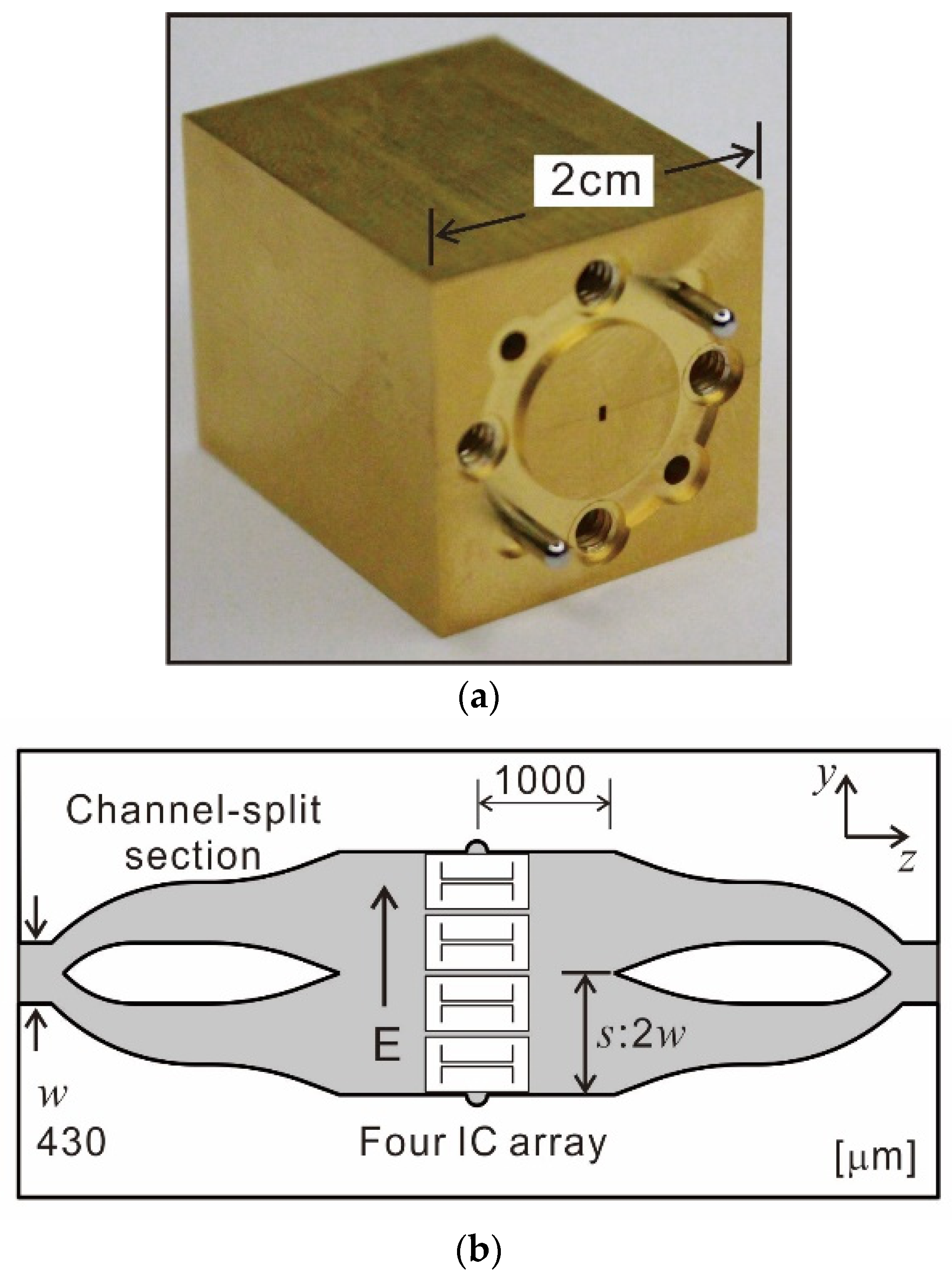
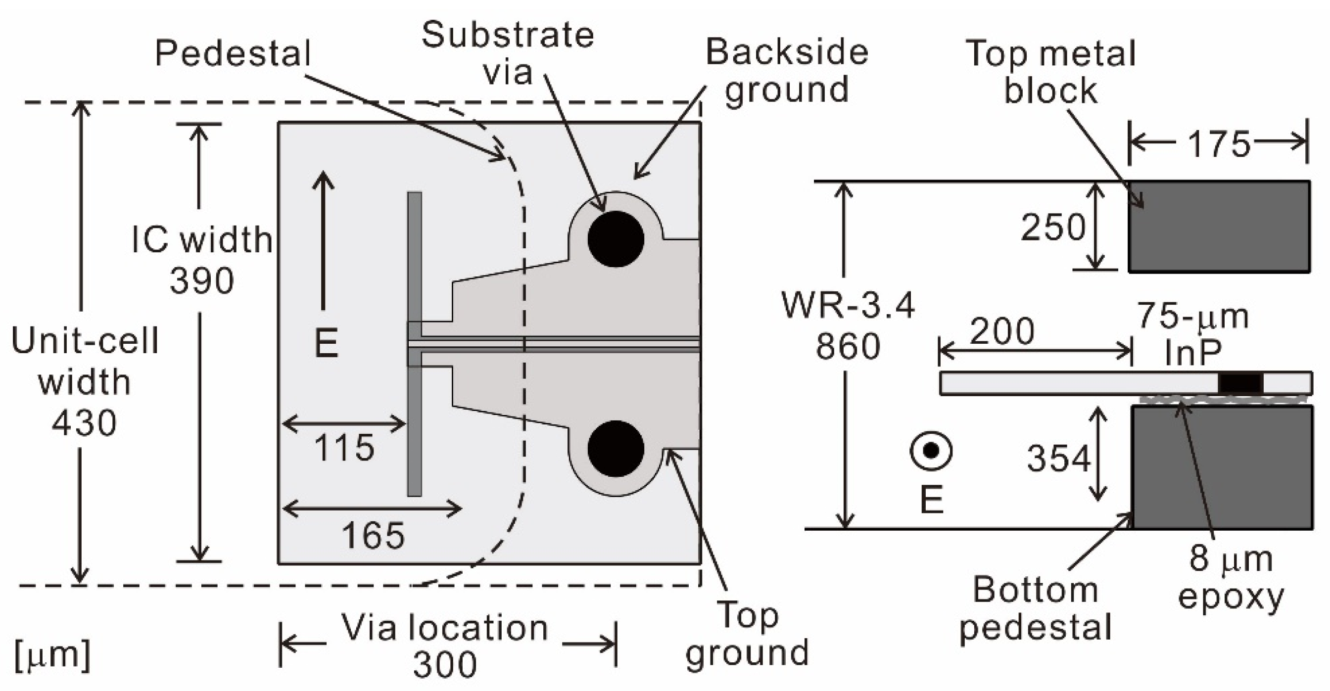
2. Array Module Assembly

A sketch and photograph of the terahertz waveguide module containing a linear array of four IC chip elements are shown in Figure 1. Waveguide machining becomes very challenging when the frequency reaches the WR-3.4 band; the standard waveguide E-plane width (w) is only 430 mm because the size of available milling tools is only 200 mm. This forces the waveguide machining tolerance to exceed 20 mm. For the channel-split section inside the module, the channel widths are continuously varied without sharp corners to achieve a minimum reflection loss over a wide frequency range. The narrowest channel width near the split junction is 215 mm, slightly larger than the size of the milling tool. In the final stage of the binary tree before the two channels are merged, a cosine taper is applied to increase the channel width (s) to 860 mm, the largest single-channel width that prevents the propagation of higher-order modes.
In our experiment, the IC chips received the incoming power from the input waveguide and retransmitted it into the output waveguide using a pair of broadband transition antennas. These through-line IC chips were fabricated using Teledyne’s 250 nm DHBT technology. As shown in Figure 2, the IC chip widths were fixed at 390 mm to operate with an air-gap margin of 20 mm on each side inside the unit cell, having a width of 430 mm. When the air-gap sizes were increased to over 40 mm, the operation bandwidth became narrower, and ripples started to appear in the frequency response of the module. Although the transition dipole was similar to that already introduced in [13], its design was improved to achieve a wider operation bandwidth. The metallic pedestal working as a back-short reflector for the dipole provided reactance matching while ensuring a full isolation between the input and the output of the waveguide. The number of available IC chips is limited; therefore, only four chips were mounted across the overmoded E-plane channel with a width of 1720 mm. Accurate chip positioning on a waveguide pedestal is a difficult and often unrepeatable task. In addition, we found that the amount of electrically conductive epoxy underneath the chip, EK2000 from Epoxy Technology, may have influenced the module performance. Therefore, three different array modules were assembled to check the repeatability in the chip mounting process.

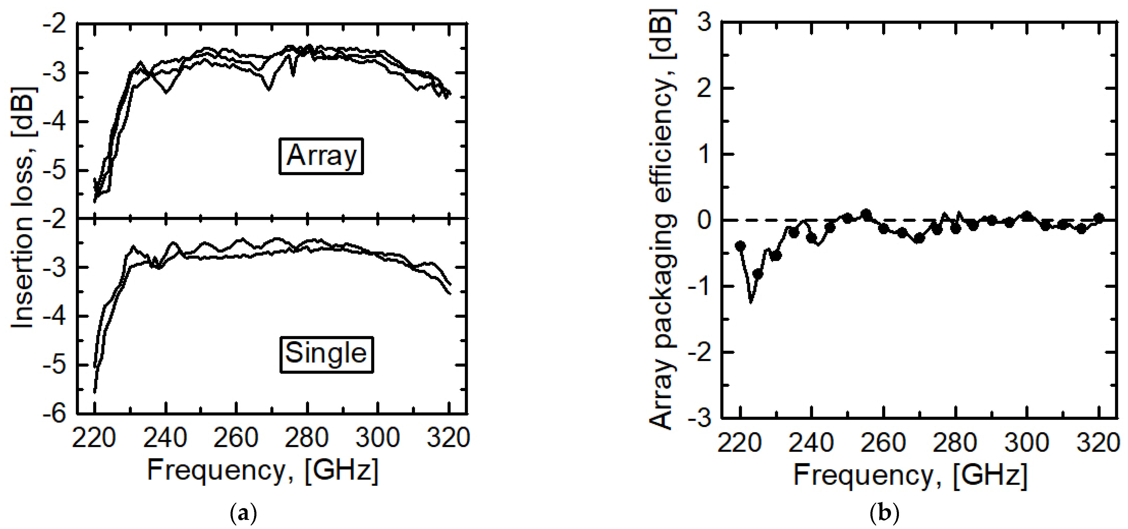
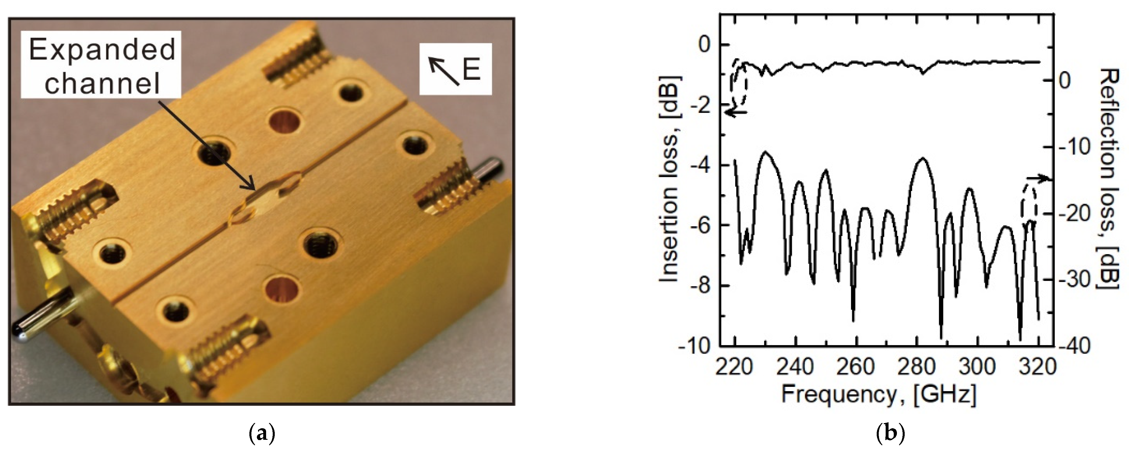
3. Array Module Performance

A total of five separate modules, three array modules along with two single-element modules, were fabricated and tested using a WR-3.4 vector network analyzer. All three array modules possessed almost identical small-signal responses with less than 0.5 dB module-to-module variations, possessing roughly 3 dB of insertion loss across the full WR-3.4 band, as shown in Figure 3a. In addition, no sharp resonances or reflections normally seen in waveguides with their channel widths exceeding 1.5 wavelengths at 270 GHz were observed. This indicates that the unit-cell symmetry and single-mode propagation are well preserved across the expanded E-plane channel, even with the multiple chip mounting process. Two additional modules containing only a single IC chip were built for comparison purposes; their small-signal responses are also included in Figure 3a. The performance of both types of modules was in accordance with the simulation results from High Frequency Structure Simulator (HFSS from Ansoft) when a metal conductivity of 1.3 × 10⁷ S/m for the waveguide walls and microstrip conductors was assumed. The measured results exhibited a slight upward frequency shift in the operation bandwidth because the initial IC design used a higher dielectric constant of 12.8 as opposed to the corrected dielectric constant of 11.8.
The array packaging efficiency calculated from the difference between single and array module’s average insertion losses is plotted in Figure 3b. It shows there are no significant additional losses for the entire frequency band for the array modules, except the small extra losses near 220 GHz and 270 GHz. These results imply that the amplifier gain will be preserved, whereas the output power will increase by a factor of the number of array elements when amplifier ICs are packaged instead of through-line ICs.

4. Field Uniformity Test

An empty module, shown in Figure 4a, with both the IC chips and the pedestal removed from the expanded E-plane channel was machined for the extra verification of a uniform field distribution across the 1720 mm wide channel. The measured insertion and reflection losses covering the full WR-3.4 band are plotted in Figure 4b. The average insertion loss was roughly 0.7 dB, and the mismatch loss stayed below −10 dB for the entire band. The flat insertion loss without large reflections indicated that the uniform-amplitude TE10 mode was well preserved in the expanded channel.
Another array module cut in the middle to form an open-end waveguide, as shown in Figure 5a, was additionally tested for radiation patterns, following the approach introduced in [5]. The expanded E-plane channel directly facing the free-space was an efficient radiator, working as an E-plane horn with a uniform phase. The measured reflection coefficient of the open-end block was less than −10 dB for the full band. The measured E-plane pattern at 270 GHz plotted in Figure 5b shows a half power beamwidth of 34 degrees and a side-lobe level of 12 to 14 dB, indicating a source aperture with a uniform amplitude and sharp edges. The pattern matched very closely to the normalized sinc function that represents the radiated pattern from a uniform-field source with an aperture size of 1720 mm. The measured H-plane pattern also matched well with a theoretical pattern obtained from the Fourier transform of a half-cycle cosine field variation across an 860 mm aperture which was multiplied by the obliquity factor of cosq for the radiating aperture placed on top of a metallic surface

5. Conclusions

The waveguide module presented in this paper delivers and collects uniform power to and from an array of IC chips located inside a metallic packaging environment for frequencies as high as 300 GHz. The measured results confirm that the small-signal performance of the array modules very closely followed performance of single-element modules, indicating that the power performance will improve by the number of elements packaged in the module. The expanded E-plane channel technique becomes truly advantageous over the separate-channel approach when all the array elements are fabricated together on a single chip. It remains the target of future research to fabricate a linear array of amplifier elements together with DC bias circuitry on a single chip.

Author Contributions

Investigation, data curation, and original draft preparation, J.L.; housing fabrication and assembly, and data curation, Y.W.K.; supervision, project administration, and funding acquisition, S.J. and M.K. All authors have read and agreed to the published version of the manuscript.

Funding

This work was supported by Samsung Research Funding & Incubation Center of Samsung Electronics under Project Number SRFC-IT2002-08. The chip fabrication was supported by the IC Design Education Center (IDEC), Korea.

Conflicts of Interest

The authors declare no conflict of interest.

References

  1. Yu, H.G.; Choi, S.H.; Kim, M. 300 GHz InP HBT Amplifier with 10 mW Output Power. IET Electron. Lett. 2014, 50, 377–379. [Google Scholar] [CrossRef]
  2. Kim, J.; Jeon, S.; Kim, M.; Urteaga, M.; Jeong, J. H-Band Power Amplifier Integrated Circuits Using 250-nm InP HBT Technology. IEEE Trans. Terahertz Sci. Technol. 2015, 5, 215–222. [Google Scholar] [CrossRef]
  3. Ahmed, A.S.H.; Soylu, U.; Seo, M.; Urteaga, M.; Rodwell, M.J.W. A Compact H-band power amplifier with high output power. In Proceedings of the 2021 IEEE Radio Frequency Integrated Circuits Symposium (RFIC), Atlanta, GA, USA, 7–9 June 2021; IEEE: Piscataway, NJ, USA, 2021; pp. 123–126. [Google Scholar]
  4. Urteaga, M.; Griffith, Z.; Seo, M.; Hacker, J.; Rodwell, M.J.W. InP HBT Technologies for THz Integrated Circuits. Proc. IEEE 2017, 105, 1051–1067. [Google Scholar] [CrossRef]
  5. Wang, T.; Ning, Y.; Zhu, W. Design of an E-band power amplifier based on waveguide power-combining technique. In Proceedings of the 2018 International Conference on Microwave and Millimeter Wave Technology (ICMMT), Chengdu, China, 7–11 May 2018; IEEE: Piscataway, NJ, USA, 2018; pp. 1–3. [Google Scholar]
  6. Dang, Z.; Zhu, H.-F.; Huang, J.; He, H.-D. An Ultra-Wideband Power Combining in Ridge Waveguide for Millimeter Wave. IEEE Trans. Microw. Theory Tech. 2020, 68, 1376–1389. [Google Scholar] [CrossRef]
  7. Radisic, V.; Leong, K.M.K.H.; Sarkozy, S.; Mei, X.; Yoshida, W.; Liu, P.-H.; Deal, W.R.; Lai, R. 220-GHz Solid-state Power Amplifier Modules. IEEE J. Solid-State Circuits 2012, 47, 2291–2297. [Google Scholar] [CrossRef]
  8. Rollin, J.-M.; Miller, D.; Urteaga, M.; Griffith, Z.M.; Kazemi, H. A Polystrata 820 mW G-band Solid-state power amplifier. In Proceedings of the 2015 IEEE Compound Semiconductor Integrated Circuit Symposium (CSICS), New Orleans, LA, USA, 11–14 October 2015; IEEE: Piscataway, NJ, USA, 2015. [Google Scholar]
  9. Gritters, D.; Brown, K.; Ko, E. 200–260 GHz solid state amplifier with 700 mW of output power. In Proceedings of the IEEE MTT-S International Microwave Symposium, Phoenix, AZ, USA, 17–22 May 2015; IEEE: Piscataway, NJ, USA, 2015; pp. 1–3. [Google Scholar]
  10. Yi, C.; Cho, J.; Shin, J.; Kim, M. 260-GHz Waveguide Module Containing an Integrated InP HBT Amplifier Chip. Electron. Lett. 2020, 56, 665–667. [Google Scholar] [CrossRef]
  11. Maaskant, R.; Shah, W.A.; Zaman, A.U.; Ivashina, M.; Kildal, P.-S. Spatial Power Combining and Splitting in Gap Waveguide Technology. IEEE Microw. Wirel. Comp. Lett. 2016, 26, 472–474. [Google Scholar] [CrossRef] [Green Version]
  12. Yi, C.; Lee, H.; Lee, K.J.; Joo, J.H.; Kwon, J.B.; Kim, M. Uniform-field Over-mode Waveguide for Spatial Power-combining Applications. IEEE Microw. Wirel. Comp. Lett. 2018, 28, 10–12. [Google Scholar] [CrossRef]
  13. Yi, C.; Lee, K.M.; Kim, H.J.; Kim, M. WR-3.4 InP HBT Amplifier Module with Integrated Wideband Waveguide Transitions. IEEE Microw. Wirel. Comp. Lett. 2021, 31, 1315–1318. [Google Scholar] [CrossRef]
Figure 1. WR-3.4 waveguide module containing four-element IC array. (a) Photograph of the fully assembled waveguide module; (b) E-plane sketch of the middle expanded-channel section; (c) photograph of the split module showing the expanded-channel section.
Electronics 11 02091 g001aElectronics 11 02091 g001b
Figure 2. E- and H-plane views of the IC chip mounted in the unit cell.
Electronics 11 02091 g002
Figure 3. Measured array module performance. (a) Insertion loss comparison with the single-element modules; (b) average loss difference from the single-element modules.
Electronics 11 02091 g003
Figure 4. Empty array module test. (a) Photograph showing the bottom half of the empty module; (b) measured insertion and reflection losses.
Electronics 11 02091 g004
Figure 5. Open-end array module test. (a) Photograph showing the bottom half and the fully assembled open-end module; (b) measured (solid) and theoretical (dashed) E- and H-plane patterns.
Electronics 11 02091 g005
Publisher’s Note: MDPI stays neutral with regard to jurisdictional claims in published maps and institutional affiliations.

