Abstract
We present the optical modelling of a mesoporous fibre perovskite solar cell (PSC). It was conducted by means of the transmission line method (TLM), which was used to calculate the efficiency and short-circuit photo-current density of the cell. The TLM was first applied for a planar mesoporous PSC and verified with the experimental results from the literature. Numerical calculations for both planar and fibre PSC were conducted and analysed regarding their efficiency in terms of optical simulation. The importance of choosing the thin-film layers’ materials and thickness was demonstrated, and a potential improvement using anti-reflection coatings was also examined.
1. Introduction
Almost every article on third-generation photovoltaics (PVs) starts with a reference to the worldwide increasing energy demands and the need for carbon-free technology. These are actual problems, and new PV technologies can certainly help to address them [1].
Lead-halide perovskite PVs have been shown to achieve significantly increased efficiency in the last decade. Other well-developed technologies, such as organic photovoltaic (OPV), dye-sensitized and quantum-dot solar cells, have not shown such high performance [2,3,4]. This is due to the beneficial electronic and optical properties of those perovskite materials, which, most commonly, are CH3NH3PbBr3, CH3NH3PbI3 or a mixture of both. These properties are extremely interesting for engineers and scientists alike and include superior carrier mobility, diffusion length beyond 1 μm, slow charge recombination, easily tuneable bandgaps, surprising structural-defect tolerance and high optical absorption coefficients [1,2,5]. It should be added that some of these properties are not observed in bulk perovskite materials but only in thin films [6].
Moreover, manufacturing techniques for PSCs are cheaper and more environment friendly than those regarding silicon cells since the former do not include expensive materials and high-temperature processing.
Recently, fibre-shaped thin-film PVs have received their share of attention, though to a lesser extent than their planar counterparts, not only owing to their more demanding development, but also due to issues that have to be resolved regarding new-generation solar cells (SCs) in general. Fibre PVs are of cylindrical geometry, and though they have lesser efficiency under direct sunlight than similar planar PVs, they can benefit more from diffused, scattered and inclined light. Besides, those fibres could be used to create flexible surfaces of various shapes and textiles and could be easily integrated in clothing [7].
Perovskites are likely the best option for fibre PVs due to their excellent thin-film characteristics and ease of development. The dye-sensitized solar cell (DSSC) is a competing technology, and experimental results achieving photo-current density (JSC) levels of more than 17 mA/cm2 have been reported [8], which is quite impressive for a fibre PV. However, the liquid electrolytes needed in those structures make their construction much more demanding than that of fibre PSCs. The relative easiness of construction is one of the advantages of fibre PSCs, and some experimental groups have developed several different configurations, most of them with a mesoporous scaffold layer. Various types of external electrodes and fibre core materials have been tested in combination with hole- and electron-transport layers (HTLs, ETLs), selected for their beneficial electronic properties [7]. However, despite the fact that the electronic characteristics have been optimized and the efficiency of the fibre structures has been enhanced, room for improvement does exist.
In this paper, we present an optical simulation model for the evaluation of the efficiency of a mesoporous PSC with a planar or fibre geometry. The optical efficiency of such multi-layer devices depends on the complex spectral refractive indices of the materials involved and the thickness of the layers. Apart from the reflection caused by the structure, nano-scale films give rise to interference phenomena, resulting in stationary optical waves created within the layers. In order to optimize light harvesting, the intensity should ideally be at a maximum in the active medium (a), the perovskite and/or the mesoporous layer. Through the proposed modelling, an efficiency calculation may be performed regarding the optimum combination of the material and the thickness of the structures’ layers. Therefore, there is a strong motivation for the optical modelling of both planar- and fibre-geometry PSCs.
Optical models have already been used for either conceptual or experimental PSCs, employing the transfer matrix method (TMM) [9,10,11,12]. However, to the best of our knowledge, the optical modelling of fibre PSCs has not been reported.
For the optical modelling of both geometries, the transmission line method (TLM) was adopted. The TLM provides physical insights, embodies complex refractive indices, index anisotropy and nonlinearity, and at the same time, it is fast and easy to implement [13,14]. Details on the method used are provided below. The application of the TLM was verified for a planar structure by calculating the external quantum efficiency and the short-circuit photo-current JSC. A specific planar structure was considered that presented similarities with respect to the fibre one with a mesoporous and a perovskite capping layer. The model was also used to evaluate a possible enhancement of the efficiency of a fibre PSC that incorporates a conceptual anti-reflection coating. Both structures have been the subject of already published experimental works, and details are given in the next section.
2. The Modelled PCS Structure
Instead of simulating a conceptual device, we tried to model two existing stacks found in the literature, one planar and one cylindrical. That choice was made to enable a comparison with available experimental results as a baseline to present the usefulness of optical modelling, as well as to propose possible variations and additions to the cylindrical stack that could improve similar fibre PSCs. These issues are discussed in Section 4.
The planar SC is of the n-i-p configuration type, while the cylindrical one is of the inverted p-i-n one, more common in fibre SCs. However, both structures have a mesoporous layer, which is also common in fibre PSC architectures. Another important reason for choosing the specific planar stack was the availability of relevant optical data, at least in part [15]. The optical modelling method employs the material refractive index and the thickness of the layers; however, the necessary data are rarely included in publications of experimental groups. Moreover, the thin films formed from the novel materials in use have optical characteristics that differ from the ones of known bulk materials and are also affected by the method of preparation and film deposition.
We first modelled the planar structure by using data provided in the literature. Figure 1 depicts the schematic of the structure’s configuration. The specific references are given in the Results section, but it has to be mentioned that the refractive index of a given thin-film material from the literature can vary up to 30% in some spectral ranges (see, for example, [16,17]). Nevertheless, the most important material index is that of perovskite (the active material), and this was indeed provided in [5]. The choice of somewhat different indices for other films, such as the electron transport layer (ETL), can result in variations in the measured performance; these, however, are no more than 5%. The general picture of the device’s performance is very effectively approached by this simulation method.
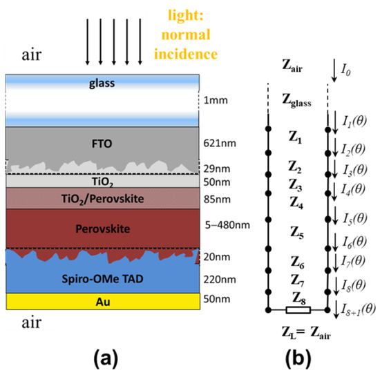
Figure 1.
(a) The simulated planar photovoltaic structure. (b) The equivalent transmission line model.
The next structure we modelled (which is the most important one) was cylindrical and was based on the best-performing fibre PSC. However, the lack of exact optical data was more challenging in this case [18]. Hence, we had to use data from other sources in the literature and also make some necessary assumptions. Moreover, the thickness of each layer was only approximately calculated. We had to rely on the SEM images from the article since the thicknesses of the layers were not specifically given. Depending on the position of a layer, either before or after the active layer (with regard to the direction of sunlight), small variations in its thickness may have some effect on the device, though not considerable ones.
Another issue that had to be addressed was the roughness of the films. These films are never perfectly polished, but if surface roughness is up to a few nanometres, it can be neglected. However, the roughness magnitude is sometimes quite higher, with RMS of tens of nanometres [19]. It also happens that surface roughness depends on the material itself and obviously on the method of layer deposition [20]. This roughness on the interface of tandem layers makes the two materials blend together, effectively creating another layer in between. The roughness between layers was included in both modelled structures (where necessary), and it was modelled using the Bruggeman effective medium approximation (EMA). For the EMA approach, however, the magnitude of the roughness and the volume fraction of the two materials were needed, but this kind of data was not readily available in [15,18]. Hence, we had to draw the necessary data from other existing experimental or commercial sources.
The same approach of the Bruggeman EMA was adopted for the modelling of the mesoporous layer. In both structures, this was made by mesoporous TiO2 (titania), the so-called scaffold. This material was filled with the given perovskite; thus, the layer was a blend of the two materials. The porosity of titania was given in the first of the aforementioned articles to be close to 50%. Porosity was not known for the second structure, and it was also taken to be 50%. This constituted an additional assumption, though a realistic one.
A schematic of the fibre PSC structure with the stacked materials is depicted in Figure 2. The fibre was made of Ti and had a radius measured in hundreds of μm, while the PSC thickness was three orders of magnitude smaller and formed a thin cylinder film. If we divided the fibre cross-section in a number of small arcs, then every segment of the cylinder could be approximated by a planar structure. These segments were considered of infinite length along the fibre axis (y-direction) [21]. They were also considered very long along the x–z-plane in comparison with the wavelength of light.

Figure 2.
Light incidence on the cylindrical structure (which was divided in almost planar segments) and detail of a typical segment.
The incident light was considered to be a plane wave, consisting of TE and TM waves (s- and p-polarisations) in equal amounts, normal to the fibre axis. The light illuminated only the upper half of the cylindrical surface, having a different angle of incidence θ on each segment. In the case of normal incidence, the two polarizations were treated similarly, but if , TE and TM waves had to be treated separately [22].
3. Modelling Method
The TLM has been used to model inclined light incidence and propagation through thin-film structures [22]. The method treats the light propagation in the structure as a 1D transmission line problem and is ideal for problems of electromagnetic propagation where coherent interactions form standing waves through a multi-layered stack. It has also been successfully used in cases such as the modelling of partial coherent and incoherent interactions, of materials with nonlinear refractive indices, etc. [13,14]. We briefly present the method. The reader might also check the above references for a more detailed description.
To calculate the electric field and the light intensity in a multilayer structure under illumination, as in our two examples, each layer is modelled with an equivalent transmission line with its own characteristic impedance and transmission constant. In Figure 1b, these equivalent transmission lines connected in tandem are shown for the planar structure. For N layers, each layer (and line) is given an index from 1 to N. This index is used to distinguish the i-th layer’s thickness , dielectric coefficient , index of refraction , etc. We use “0” and “N + 1” to depict the semi-infinite media in front of and beyond the structure. For the first of the two stacks modelled, there was air at the front and back; for the second, there were air at the front and titanium fibre at the back.
For a given angle of incidence θ, light is considered as a sum of monochromatic plane waves having field components of form . Their spatial Fourier transform along the x- and y-directions is depicted as . Thus, after transforming the Maxwell equations into the (spatial) Fourier space, the six field components of the EM waves are depicted as and . Then, we can define the magnetic (M) and electric (E) transmission lines, representing the propagation of Fourier-transformed TE and TM waves, respectively [22]. The magnetic and electric voltage and current along the lines are given by:
In order to calculate the voltage and current transmitted in layer “1”, the following relations are employed:
where the “0” index depicts the incident current and voltage (EM field) and is the reflection coefficient for a magnetic or electric line, as needed:
where Z is the characteristic impedance and Zin the input impedance of the equivalent for the layer transmission line, either magnetic or electric. Without giving too many details, it suffices to say that these quantities are given by algebraic relations, easily calculated by a personal computer.
According to the TLM, the current and voltage at any point z inside the i-th transmission line and, equivalently, the corresponding layer are defined by the following relations:
Symbols Ii+1 and Vi+1 represent the current and voltage between line i and I + 1 lines and are calculated in a similar way, while the transmission constants along the semi-infinite x–y-plane and the z-direction are defined by:
For isotropic layers, it is . We can also define a horizontal wavenumber ku as:
where . Since the incident medium is lossless, ku is constant throughout the structure, according to Snell’s law.
The above analysis shows that the propagation of TE or/and TM waves through the PV multilayer stack is modelled by the currents and voltages along a series of equivalent magnetic or/and electric transmission lines. Furthermore, the length, impedance and transmission constant of each line depend on the material refractive indices, as well as on the incident angle and the wavelength. The semi-infinite bulk material at the back of the stack is represented by its characteristic impedance and is the final load at the end of the transmission line series (Figure 1b).
For the problem at hand, with light illuminating the stack with angle θ and being normal to the y-axis, as in Figure 2, the electric field intensity inside the stack can be calculated as follows [22]: For TE waves (waves with s-polarization), due to the equivalence of the field intensity in the Cartesian space with that in the Fourier space, we have:
In the case of TM waves (p-polarization) the field intensity is given by . As above, it can be similarly expressed as:
In order to examine the efficiency of photovoltaic solar cells (PVSCs) such as the two stacks we present here, we need to calculate their external quantum efficiency (EQE) and the short-circuit photo-current density. These quantities are proportional to the field intensity inside the active layers of the stack. Hence, the number of excitons generated at a given point inside the active layers is proportional to the current and voltage of the equivalent transmission lines at the same point [23,24]. It has been shown that the time-averaged energy absorbed in a given layer i can be expressed by:
where and are the real and imaginary parts of the refractive index. If denotes the same quantity but with the TM and TE intensity components normalized to the corresponding components of the incident electric filed, the EQE can be calculated as the average energy dissipated inside the active layers relative to that dissipated through the whole of the N-layer stack through the following expression:
Indices P and mp denote the two active layers, that of the pure perovskite and the mesoporous layer. Term (1 − T) represents the power transmitted through the stack and lost. It must also be noted that the averaged intensity involved is the one transmitted through the multilayer stack, while the reflected part is also here considered as a loss.
In the case of the studied cylindrical PSC, the surface discretization shown in Figure 2 is used. Each case of different incidence angles is solved separately and is used to calculate the average energy dissipated in an active layer as:
Finally, if the source is the sun or one that simulates sunlight, with power density spectrum Pin(λ), the photo-current density produced from the two active layers can be expressed as:
where the proportion of incident light lost to the PV cell due to reflection or transmission is considered.
It has to be mentioned that without having insight into the specific electronic characteristics of each stack, we assumed that all the excitons created in the active layers managed to reach their electrodes. This would imply a maximum Internal Quantum Efficiency (IQE = 1) and that the maximum current was generated for a given stack. Well-constructed PSCs have actually reported high values of efficiency, mainly due to the beneficial characteristics of perovskite materials such as their diffusion length, which can reach 1 μm, their superior carrier mobility, etc. [1,2,5].
However, the mesoporous layer in the stack was actually a mixed layer consisting of the porous TiO2 scaffold filled with perovskite. The refractive index of a layer is indeed a combination of the indices of both materials and their volume fractions, but the electrically useful light should only be that absorbed by the perovskite material. To have a better approximation of the actual efficiency of the mesoporous layer, we used a correction factor, also used in a similar, previous work [25]. The corrected averaged energy would be:
Indices mp and mp-perov indicate the active mixed mesoporous layer and the mesoporous material devoid of perovskite:
4. Optical Simulation Results and Discussion
In this section, we show the application of the TLM on the above-mentioned planar and fibre PSCs with the aim to evaluate the optical efficiency of a specific fibre PSC. In order to evaluate the applicability of the TLM, a planar PSC was first modelled, since for that specific structure experimental data were available. Though the two structures employed different perovskite materials, the planar PSC showed similarities with the fibre one, since both structures had two active layers, one formed by perovskite and the other made up by mesoporous titania filled with perovskite material.
4.1. The Planar Structure
As a planar structure to be simulated, the structure of [15] was selected. This was an n-i-p cell where the light was incident through a thick (1 mm) glass substrate, coated by a layer of FTO, which was the transparent electrode, around 650 nm thick. Additionally, a 30 nm layer of SnO2 was considered between the glass and the FTO, since it is commonly used with FTO glass such as TEC 7 and TEC 15 [9,26]. These were followed by 50 nm ETL compact TiO2 and 85 nm of mesoporous TiO2 filled with perovskite (see Figure 1). Next, there was the perovskite “capping” layer (for which various thickness values up to 500 nm were used) followed by the HTL made of Spiro-OMeTAD with a thickness of 240 nm and the gold back-electrode, which was 50 nm thick. We also modelled two layers of roughness, that of FTO (29 nm) bordering with TiO2 and that of Spiro-OMeTAD (20 nm) bordering with perovskite. Although the values for the roughness were not provided, thin films of those materials are known to possess a measurable level of roughness depending on the deposition method. The extent of their roughness was estimated according to the literature [9,20,26,27]. The perovskite material was of a mixed type, specifically created for [15], and all its optical characteristics were provided therein.
The spectral complex refractive indices of all layers were either extracted from the aforementioned article or were drawn from other works with similar thin films [9,15,17,28]. Direct illumination from 400 to 800 nm under AM1.5 conditions was assumed. The light was assumed to be impinging normally on the glass substrate, and no indirect illumination was considered.
As a first result, the EQE of the planar PV stack is shown in Figure 3 for the spectral range involved. The thickness of the perovskite capping layer was set to 480 nm. This efficiency figure of merit is rather typical for a PSC, with relative lower efficiency at shorter wavelengths, the highest efficiency observed from 500 to 700 nm and a steep drop after. There was an evident similarity with respect to the experimental results that illustrates the importance of optical effects.

Figure 3.
EQE vs. wavelength for the planar structure.
Furthermore, photo-current density JSC of the planar device was calculated for various values of the perovskite layer thickness, while the thickness of the mesoporous layer was kept constant. The results are shown in Figure 4.

Figure 4.
JSC vs. perovskite layer thickness for the planar structure.
By comparing these results with the experimental ones, small discrepancies were observed. Particularly, for a perovskite thickness of 480 nm, we calculated JSC = 24.28 mA/cm2, while the respective experimental value was 23 mA/cm2 [15]. Taking into account the lack of certain data regarding the device, such as the material layers of the glass electrode, exact roughness measurements and, most importantly, the exact values of the spectral complex refractive index for each film, the above deviation was considered reasonable.
It should be mentioned that, based on the data for the refractive indices, all thin-film layers were considered isotropic. However, TiO2 that was formed in compact thin films could be either of the amorphous or of the anatase type, with the latter one being anisotropic. Hence, the question arises if this should be included in an optical model, even though this information is not available for the aforementioned planar or cylindrical stack. According to the literature on titania thin films, anisotropy depends on the preparation method, but it is rarely reported, probably because it is not of a considerable degree [29,30,31]. Moreover, there is the question of whether a small degree of anisotropy in a layer less than 100 nm thick would make any difference in the efficiency of the device. Nevertheless, the anisotropy of the compact TiO2 layer was embodied by using the spectral refractive indices measured in another experimental work, while the mesoporous layer was still considered isotropic because of its amorphous nature [31,32]. The results differed from the ones shown in Figure 4 by only a very small margin, which is why we did not include anisotropy in either of the two modelled stacks.
Focusing more on the device’s performance, the distribution of the optical electric field inside the layers had to be calculated. In Figure 5, the intensity of the normalized electric field inside this planar PSC is shown for the spectral range under consideration. Light was incident on the FTO, and the thickness of the structure is shown on the y-axis. Each layer is depicted at the point placed from the top to the bottom of the structure so that their relative thickness is presented. On the right y-axis, the positions are also shown in nm. There was no significant loss in the FTO layer, while for most wavelengths light energy was absorbed in the mesoporous and the perovskite layers, which resulted in a rapid decrease in the light intensity. This is a result similar to those presented in other modelling works employing the TMM and concerning similar n-i-p PSCs [9,12]. In these works, though only a limited number of wavelengths were considered, it was also shown that light intensity rapidly decreased inside the perovskite layer (obviously due to the high absorption coefficient of these materials). In comparison, the TLM modelling of a planar OPV revealed the existence of standing waves inside the blend of P3HT and C70-PCBM. However, while having intense maxima inside the active media is a proof of successful optical design of the SC, it is also an indication of a smaller absorption coefficient [22].
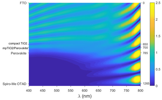
Figure 5.
Distribution of the electric field intensity inside the planar structure. The thickness of the perovskite layer was 480 nm.
For longer wavelengths, standing waves are more intense, but there is progressively less absorption. This is to be expected because the active layers have very low absorption coefficients at those wavelengths.
4.2. The Cylindrical Structure
Next, by using the TLM, we simulated the cylindrical structure after an initial verification with the experimental results. Next, we evaluated its characteristics and optimized its efficiency by applying certain alterations in its layers and structure. The current density was calculated for various thicknesses of the perovskite, ETL and HTL layers, while we evaluated a potential improvement through the use of an external capping layer.
The thin-film layers that were used in the model (also shown in Figure 2) were a gold nanoparticle (GNP) electrode (24 nm), the HTL made of Spiro-OMeTAD (100 nm), an interface roughness layer (20 nm), the CH3NH3PbI3 perovskite layer (500 nm), the mesoporous TiO2 layer (100 nm) and the titanium fibre substrate. The above values were roughly estimated from the SEM images provided in [18]. The refractive indices of the specific thin films were not available either; hence, their values used in the model were found in the literature [9,16]. Direct illumination from 350 to 900 nm under AM1.5 conditions was assumed to match the conditions of the respective experiments.
A special reference has to be made for the modelling of the GNP electrode. This film was reportedly created by the sputtering method and had NPs with sizes from 20 to 50 nm [18]. Depending on the spattering time and other preparation parameters, GNP films used as semi-transparent electrodes are discontinuous, formed of nano-islands and of statistically varying thickness. The NPs are also not spherical but of various shapes (oblate, rod-like, triangular, etc.) and sizes, as it has been stated [33,34,35,36]. In conclusion, this film can be viewed as a roughness layer, made of uneven Au structures and being a mixture of Au and air. It is also known that the dielectric constant of large NPs, such as the aforementioned ones, is very close to that of bulk Au [36]. Therefore, the Bruggeman ΕΜA can be used to model the optical response of such a layer. To model such an uneven surface, three successive EMA layers were chosen for increasing the Au volume fraction from top to bottom. The best fitting was achieved for the air: Au fractions of volume 90:10/80:20/70:30. The three virtual layers were set to be of 8 nm thickness each. These are depicted in Figure 6.

Figure 6.
Conceptual picture of the GNP electrode layer and its division in three virtual layers of increasing Au volume from top to bottom.
The transmittance measurements of such electrodes regarding the creation of fibre PSCs were reported in [37]. By simulating those measurements, we concluded the three above-mentioned EMA layers. The transmittance of this virtual electrode is shown in Figure 7 and was in good agreement with the experimental results in [37].

Figure 7.
Transmittance of the modelled Au top electrode.
Having determined the optical characteristics of the top electrode, we proceeded with the efficiency calculations of the fibre PSC. In Figure 8, a 3D plot of the photo-current density versus the thickness of the perovskite and of the Spiro-OMeTAD layers is shown. It can be seen that for specific values of the thicknesses of the above-mentioned layers, JSC was almost 10.3 mA/cm2, while the best experimental results were between 9.46 and 14. 18 mA/cm2 [18]. In that work, the authors conducted several experiments, varying the preparation method and ultimately creating a perovskite material of improved crystallization, substantial grain size and forming films with enhanced uniformity. That means that the optical properties of their perovskite layer could not be exactly the same as those of the one we used. The deviation of the TLM result also stemmed from the lack of exact optical data for the device in general. In order to test the precision of the method, we used somewhat different indices for the HTL and ETL layers, also found in the literature, and we also modelled the top electrode as a very thin but continuous gold layer. The amount of JSC was, then, somewhat different, but its dependence on the thickness of perovskite and HTL was very similar to that in Figure 8. Despite the difference from the best reported value, the TLM result was still in the high end of the values measured in the work mentioned [18].

Figure 8.
JSC of the fibre structure for varying perovskite and HTL layer thicknesses.
More conclusions can be drawn from the results in Figure 8. The current did increase with the increase in the thickness of the perovskite layer above 100 nm, but not much. It seemed that the larger proportion of light intensity had already been absorbed. In addition, by having a thinner HTL, the current could only increase by a small margin. This is understandable, since the HTL was above the active layers in this structure. At the same time, a thicker (up to 300 nm) HTL, caused a rather small drop in the current density. As shown in Figure 10, a standing wave was formed within the electrode and the HTL layer, which depended on the difference between their refractive indices and that of perovskite, which formed the next layer. Although its amplitude within the HTL only slightly decreased (owing to the layer’s relatively small absorption coefficient), the optimal thickness of that layer, from an optical-efficiency perspective, could only be determined via analysis, as shown herein. Smaller or larger values of HTL thickness are not presented since they do not have practical importance. A very thin HTL would risk short-circuiting the cell, and a thicker one would increase the series resistance [38]. Hence, it would be best, also from an optical perspective, to build the HTL of the specific structure around 100 nm thick.
We also investigated the effect of the ETL (compact TiO2) on the generated current. We do not present the results here, but its thickness was not found to be optically important. By varying the thickness of that layer between 50 and 300 nm, Jsc was only marginally altered. This is considered reasonable, since perovskite is highly absorbing at a large range of the used spectrum, and at the same time, it is followed by the mesoporous layer, which has relatively high absorption. As a result, only a small fraction of the original light intensity passed through to the ETL, which shows an obvious similarity to the relative insignificance of the HTL thickness on the optical performance of an n-i-p PSC [12,39].
In Figure 9, the evaluated dependence of JSC on the thicknesses of the perovskite and mesoporous layers is shown. The mesoporous layer did absorb some of the light, but its optical importance decreased as the thickness of the perovskite layer increased. This is due to the pure perovskite layer being in front of the mesoporous one; thus, it absorbed most of the light before it could reach the lower layer. Still, the mesoporous layer did contribute to the overall optical efficiency. However, increasing its thickness beyond 400 nm is usually not recommended because it might hamper the charge transfer [40].

Figure 9.
JSC of the fibre structure for varying perovskite and mesoporous layer thicknesses.
In order to obtain better insight into the optical efficiency of the device, the normalized intensity of the electric field had to be examined. In Figure 10, the field intensity developed in the stack, for θ = 0, versus the wavelength is depicted, while on the left side, the relative thickness of the thin-film layers is shown. Only a planar segment of the structure was considered to allow a comparison with the one in Figure 5 to be conducted.

Figure 10.
Distribution of the intensity of the electric filed inside the structure for normal-only incidence.
It can be seen that a large proportion of the light intensity was absorbed within the gold electrode and also that the large index difference between the electrode and the HTL on one hand and the perovskite layer on the other created a high local maximum inside the HTL, which means that some less desirable absorption also occurred there. The standing wave formed in these two top layers was similar to the standing wave formed within the ETL in the n-i-p structure (Figure 5); however, here, it had a relatively higher intensity, and that degraded the efficiency of the device. On the other hand, it could be also seen that the high absorption coefficient and the large size of the perovskite layer helped to absorb all the remaining light even up to 700 nm. If the field had been more intense within this layer, then more light could have been converted to excitons (resulting in a higher current); however, this would have probably required an alternative electrode to Au, that is, a different device.
A metal electrode, even one made of GNPs, creates significant reflection loss and also absorbs a proportion of the light intensity. However well-constructed and efficient a fibre PSC may be, there is room for improvement by making a more optically efficient design. A possible improvement is the use of an anti-reflection coating. This is commonly used in planar PVs and is usually a thin-film layer of a low-loss dielectric material with an intermediate refractive index to match the difference between the air and the electrode. More recently, composite anti-reflection coatings have been proposed, made by synthesizing a transparent dielectric with metal or silica NPs [41,42,43].
We propose two conceptual configurations as alternatives to the above-modelled fibre PSC stack. The only change was the addition of an anti-reflection layer, and the efficiency was calculated by means of the TLM. The first configuration had the simple addition of a dielectric coating above the electrode. The nature of the GNPs, creating a rough surface, would make this difficult to implement without the two materials merging together, but, for completeness, the results are presented below.
In Figure 11, the JSC of the fibre PSC with the addition of a dielectric coating is presented. The results are shown for various values of the thickness and the refractive index of the additional layer. The layer was considered lossless, a realistic assumption if we consider a thin layer such as glass or silica, while the thicknesses of the fibre PSC layers were kept constant. It can be seen that a 100–150 nm capping layer made of a semi-transparent material (e.g., compact silica) would be beneficial and enhance the current density by 2–3%. By using a composite material, such as mesoporous silica, with a lower refractive index, the enhancement would be 6–7% [44].

Figure 11.
JSC for various values of the refractive index and the thickness of a conceptual top anti-reflection layer.
Another proposal could be to create a mixed layer consisting of the GNPs and a low-loss dielectric. The discontinuities of the GNP electrode with be filled up with that dielectric. That same material would then be used to create a capping layer above the filled-up electrode. Mixed films consisting of transparent dielectric materials mixed with some GNPs have been proposed as anti-reflection coatings, but the volume fraction of GNPs is very small. Here, reversing that logic, we propose a conceptual electrode of rough Au non-continuous formations with the gaps being filled with a dielectric material.
The results are illustrated in Figure 12. Again, JSC was calculated for various values of the index of a possible dielectric and for a possible capping layer of varying thickness. However, materials such as silica would result in a 7–8% degradation of the generated current. Since the capping layer would cover the rough Au surface, a possible benefit would be the improved mechanical stability of the device. A more complicated structure should be designed for a broadband anti-reflection coating, but this could be the subject of a future study.

Figure 12.
JSC for various values of n and the thickness of a conceptual “filler medium” also forming a capping layer.
5. Conclusions
A planar PSC and a fibre PSC were modelled by means of the TLM. The comparison with the experimental results from the literature showed that the model was accurate when the optical characteristics of the involved layers were available, and it appeared to be precise even when those characteristics were only approximately known. Both modelled structures had two active layers, a pure perovskite layer and a mixed mesoporous one. We calculated the EQE and the short-circuit photo-current as well as the normalized field intensity inside each structure.
The importance of certain parameters was demonstrated. To summarize, it was observed that the HTL layer was optically more important than the ETL, regarding p-i-n PSCs. An opposite but similar result has been reported elsewhere about the ETL in n-i-p PSCs. This is because, in the respective structure, each layer was before the perovskite layer; hence, together with the top electrode, it played a crucial role in the formation of standing waves, while the perovskite material, for most optical wavelengths, would most likely absorb the intensity that can reach its layer before it propagates through the layers beyond. Another observation was that the metal electrode of the specific fibre PSC caused a rather significant reduction in the light that penetrated up to the active layers. The maximum field intensity was found to be within the electrode and/or the HTL layers. Better knowledge of the specific gold NPs electrode would have certainly helped to obtain more accurate results. Two configurations of anti-reflection layers were proposed, and the simulation showed the possibility of efficiency enhancement.
Author Contributions
Conceptualization, N.M. and N.A.S.; methodology, N.M. and N.A.S.; software, N.M. and N.A.S.; validation, N.M. and N.A.S.; formal analysis, N.M. and N.A.S.; writing—original draft preparation, N.M., N.A.S. and G.P.; writing—review and editing, N.M., N.A.S. and G.P.; visualization, N.M.; supervision, N.M. All authors have read and agreed to the published version of the manuscript.
Funding
This research study received no external funding.
Conflicts of Interest
The authors declare no conflict of interest.
References
- Petrova-Koch, V.; Hezel, R.; Goetzberger, A. High-Efficient Low-Cost Photovoltaics, Recent Developments, 2nd ed.; Springer Nature: Basel, Switzerland, 2020. [Google Scholar]
- Jenat, A.K.; Kulkami, A.; Miyasaka, T. Halide Perovskite Photovoltaics: Background, Status, and Future Prospects. Chem. Rev. 2019, 119, 3036–3103. [Google Scholar] [CrossRef] [PubMed]
- Saeed, M.A.; Cheng, S.; Biswas, S.; Kim, S.H.; Kwon, S.-K.; Kim, H.; Kim, Y.-H.; Shim, J.W. Remarkably high performance of organic photovoltaic devices with 3,9-bis(2-methylene-(3-(1,1-dicyanomethylene)-indanone))-5,5,11,11-tetrakis(4-hexyl meta-phenyl)-dithieno[2,3-d:2′,3′-d]-s-indaceno[1,2-b:5,6-b′]dithiophene)-ethylhexyloxy] photoactive acceptor under halogen light illumination. J. Power Sources 2022, 518, 230782. [Google Scholar]
- Saeed, M.A.; Kang, H.C.; Yoo, K.; Asiam, F.K.; Lee, J.J.; Shim, J.W. Cosensitization of metal-based dyes for high-performance dye-sensitized photovoltaics under ambient lighting conditions. Dye. Pigment. 2021, 194, 109624. [Google Scholar] [CrossRef]
- Li, F.; Wang, H.; Kufer, D.; Liang, L.; Yu, W.; Alarousu, E.; Ma, C.; Li, Y.; Liu, Z.; Liu, C.; et al. Ultrahigh Carrier Mobility Achievedin Photoresponsive Hybrid Perovskite Films via Coupling with Single-Walled Carbon Nanotubes. Adv. Mater. 2017, 29, 1602432. [Google Scholar] [CrossRef] [PubMed]
- Sichert, J.A.; Tong, Y.; Mutz, N.; Vollmer, M.; Fischer, S.; Milowska, K.Z.; Cortadella, R.C.; Nickel, B.; Cardenas-Daw, C.; Urban, A.S.; et al. Quantum size efect in organometal halide perovskitenanoplatelets. Nano Lett. 2015, 15, 6521–6527. [Google Scholar] [CrossRef]
- Balilonda, A.; Li, Q.; Tebyetekerwa, M.; Tusiime, R.; Zhang, H.; Jode, R.; Zabihi, F.; Yang, S.; Ramakrisna, S.; Zhu, M. Perovskite Solar Fibers: Current Status, Issues and Challenges. Adv. Fiber Mater. 2019, 1, 101–125. [Google Scholar] [CrossRef] [Green Version]
- Junxiang, Z.; Zhuanpei, W.; Xuelian, L.; Jie, Y.; Chenhui, S.; Yongpeng, L.; Jianli, C.; Qun, G.; Bin, W. Flexible Platinum-Free Fiber-Shaped Dye Sensitized Solar Cell with 10.28% Efficiency . ACS Appl. Energy Mat. 2019, 2, 2870–2877. [Google Scholar]
- Ball, J.M.; Stranks, S.D.; Hörantner, M.T.; Hüttner, S.; Zhang, W.; Crossland, E.J.W.; Ramirez, I.; Riede, M.; Johnston, M.B.; Richard, H.; et al. Optical properties and limiting photocurrent of thin-film perovskite solar cells. Energy Environ. Sci. 2015, 8, 602–609. [Google Scholar] [CrossRef]
- Anaya, M.; Lozano, G.; Calvo, M.E.; Zhang, W.; Johnston, M.B.; Snaith, H.J.; Míguez, H. Optical Description of Mesostructured Organic–Inorganic Halide Perovskite Solar Cells. J. Phys. Chem. Lett. 2015, 6, 48–53. [Google Scholar] [CrossRef] [Green Version]
- Wahid, S.; Islam, M.; Rahman, M.S.S.; Alam, M.K. Transfer Matrix Formalism-Based Analytical Modeling and Performance Evaluation of Perovskite Solar Cells. IEEE Trans. Electron Devices 2017, 64, 5034–5041. [Google Scholar] [CrossRef]
- Rani, S.; Kumar, A.; Ghosh, D.S. Optical Designing of Perovskite Solar Cells. IEEE J. Photovolt. 2022, 12, 595–601. [Google Scholar] [CrossRef]
- Stathopoulos, N.A.; Savaidis, S.P.; Botsialas, A.; Ioannidis, Z.C.; Georgiadou, D.G.; Vasilopoulou, M.; Pagiatakis, G. Reflection and transmission calculations in a multilayer structure with coherent, incoherent, and partially coherent interference, using the transmission line method. Appl. Opt. 2015, 54, 1492–1504. [Google Scholar] [CrossRef] [PubMed]
- Moshonas, N.; Pagiatakis, G.; Papagiannis, P.; Savaidis, S.P.; Stathopoulos, N.A. Application of the transmission line method for the study of highly nonlinear multilayer optical structures. Opt. Eng. 2014, 53, 115106. [Google Scholar] [CrossRef]
- Correa-Baena, J.P.; Anaya, M.; Lozano, G.; Tress, W.; Domanski, K.; Saliba, M.; Matsui, T.; Jacobssom, T.J.; Calvo, M.E.; Abate, A.; et al. Unbroken Perovskite: Interplay of Morphology, Electro-optical Properties, and Ionic Movement. Adv. Mater. 2016, 38, 521–527. [Google Scholar] [CrossRef]
- Refractive Index Database. Available online: https://refractiveindex.info/?shelf=main&book=Au&page=Johnson (accessed on 25 April 2022).
- Moulé, A.J.; Snaith, H.J.; Kaiser, M.; Klesper, H.; Huang, D.M.; Grätzel, M.; Meerholz, K. Optical description of solid-state dye-sensitized solar cells. I. Measurement of layer optical properties. J. Appl. Phys. 2009, 106, 073111. [Google Scholar]
- Hsienwei, H.; Dong, B.; Chen, B.; Gao, X.; Zou, D. High performance fiber-shaped perovskite solar cells based on lead acetate precursor. Sustain. Energy Fuels 2018, 2, 79–84. [Google Scholar]
- Springer, J.; Poruba, A.; Vanecek, M. Improved three-dimensional optical model for thin-film silicon solar cells. J. Appl. Phys. 2004, 96, 5329–5337. [Google Scholar] [CrossRef]
- Wang, S.; Cabreros, A.; Yang, Y.; Hall, A.S.; Valenzuela, S.; Luo, Y.; Correa-Baena, J.P.; Kim, M.C.; Fjeldberg, Ø.; Fenning, D.P.; et al. Impacts of the Hole Transport Layer Deposition Process on Buried Interfaces in Perovskite Solar Cells. Cell. Rep. Phys Sci. 2020, 1, 100103. [Google Scholar] [CrossRef]
- Moshonas, N.; Stathopoulos, N.A.; O’Connor, B.T.; Bedeloglu, A.C.; Savaidis, S.P.; Vasiliadis, S. Optical modeling of fiber organic photovoltaic structures using a transmission line method. Appl. Opt. 2017, 56, 9351–9358. [Google Scholar] [CrossRef]
- Stathopoulos, N.A.; Palilis, L.C.; Yesayan, S.R.; Savaidis, S.P.; Vasilopoulou, M.; Argitis, P. A transmission line model for the optical simulation of multilayer structures and its application for oblique illumination of an organic solar cell with anisotropic extinction coefficient. J. Appl. Phys. 2011, 110, 114506. [Google Scholar] [CrossRef]
- Moulé, A.J.; Bonekamp, J.B.; Meerholz, K. The effect of active layer thickness and composition on the performance of bulk heterojunction solar cell. J. Appl. Phys. 2006, 100, 094503. [Google Scholar] [CrossRef]
- Pettersson, L.A.A.; Roman, L.S.; Inganas, O. Modeling photocurrent action spectra of photovoltaic devices based on organic thin films. J. Appl. Phys. 1999, 86, 487–496. [Google Scholar] [CrossRef]
- Huang, D.M.; Snaith, H.J.; Grätzel, M.; Meerholz, K.; Moul, A.J. Optical description of solid-state dye-sensitized solar cells. II. Device optical modeling with implications for improving efficiency. J Appl. Phys. 2009, 106, 073112. [Google Scholar] [CrossRef]
- 2.2 mm 7–8 Ohm/SqFTO TEC 7 Coated Glass Substrates. Available online: https://www.msesupplies.com/products/fluorine-doped-tin-oxide-fto-coated-tec-7-7-ohm-sq-glass-tec7-fto-can-customize-pattern-as-required?variant=19974123652 (accessed on 27 April 2022).
- Cojocaru, L.; Uchida, S.; Jayaweera, P.V.V.; Kaneko, S.; Wang, H.; Nakazaki, J.; Kubo, T.; Segawa, H. Effect of TiO2 Surface Treatment on the Current–Voltage Hysteresis of Planar-Structure Perovskite Solar Cells Prepared on Rough and Flat Fluorine-Doped Tin Oxide Substrates. Energy Technol. 2017, 5, 1762–1766. [Google Scholar] [CrossRef] [Green Version]
- Wenger, S.; Schmid, M.; Rothenberger, G.; Gentsch, A.; Grätzel, M.; Schumacher, J.O. Coupled Optical and Electronic Modeling of Dye-Sensitized Solar Cells for Steady-State Parameter Extraction. J. Phys. Chem. C 2011, 115, 10218–10229. [Google Scholar] [CrossRef] [Green Version]
- Essalhi, Z.; Hartiti, B.; Lfakir, A.; Siadat, M.; Thevenin, P. Optical properties of TiO2 Thin films prepared by Sol Gel method. J. Mater. Environ. Sci. 2016, 7, 1328–1333. [Google Scholar]
- Evtushenko, Y.M.; Romashkin, S.V.; Trofimov, N.S.; Chekhlova, T.K. Optical properties of TiO2 thin films. Phys. Procedia 2015, 73, 100–107. [Google Scholar] [CrossRef] [Green Version]
- Li, J.; Meng, S.; Qin, L.; Lu, H. Optical properties of anatase and rutile TiO2 studied by GGA + U. Chin. Phys. B 2017, 26, 3–8. [Google Scholar]
- Abdellatif, S.; Sharifi, P.; Kirah, K.; Ghannam, R.; Khalil, A.S.G.; Erni, D.; Marlow, F. Refractive index and scattering of porous TiO2 films. Micropor. Mesopor. Mat. 2018, 264, 84–91. [Google Scholar] [CrossRef] [Green Version]
- Lansåker, P. Gold-Based Nanoparticles and Thin Films: Applications to Green Nanotechnology. Ph.D. Thesis, Uppsala Universitet, Upsala, Sweden, 2012. [Google Scholar]
- Rai, V.N.; Srivastava, A.K.; Mukherjee, C.; Deb, S.K. Surface enhanced absorption and transmission from dye coated gold nanoparticles in thin films. Appl. Opt. 2012, 51, 2606–2615. [Google Scholar] [CrossRef]
- Summonte, C.; Maccagnani, P.; Maurizi, A.; Pizzochero, G.; Bolognini, G. Simulation of the optical properties of gold nanoparticles on sodium alginate. In Proceedings of the European Optical Society Annual Meeting (EOSAM), Rome, Italy, 13–17 September 2021. [Google Scholar]
- Haiss, W.; Nguyen, T.K.; Thanh, N.T.K.; Aveyard, J.; Fernig, D.G. Determination of Size and Concentration of Gold Nanoparticles from UV–Vis Spectra. Anal. Chem. 2007, 79, 4215–4221. [Google Scholar] [CrossRef] [PubMed]
- Hu, H.; Yan, K.; Peng, M.; Yu, X.; Chen, S.; Chen, B.; Dong, B.; Gao, X.; Zou, D. Fiber-shaped perovskite solar cells with 5.3% efciency. J. Mater. Chem. A 2016, 4, 3901–3906. [Google Scholar] [CrossRef]
- Kim, G.W.; Shindea, D.P.; Taiho, P. Thickness of the hole transport layer in perovskite solar cells: Performance versus reproducibility. RSC Adv. 2015, 120, 99356–99360. [Google Scholar] [CrossRef]
- Moshonas, N.; Stathopoulos, N.A. Optical modeling of thin film perovskite solar cells. In Novel Optical Materials and Applications; Optical Society of America: Washington, DC, USA, 2020; p. JTu4C-21. [Google Scholar]
- Zhang, W.; Anaya, M.; Lozano, G.; Calvo, M.E.; Johnston, M.B.; HernánMíguez, H.; Snaith, H.J. Highly Efficient Perovskite Solar Cells with Tunable Structural Color. Nano Lett. 2015, 15, 1698–1702. [Google Scholar] [CrossRef] [PubMed] [Green Version]
- Katagiri, K.; Yamazaki, S.; Inumaru, K.; Koumoto, K. Anti-reflective coatings prepared via layer-by-layerassembly of mesoporous silica nanoparticles andpolyelectrolytes. Polym. J. 2015, 47, 190–194. [Google Scholar] [CrossRef]
- Deka, S.; Mohammed, W. Enhancement of light absorption using Nanoparticles Embedded Double layer Anti-Reflection Coating. Eng. J. 2020, 24, 53–63. [Google Scholar] [CrossRef]
- Martínez-Hernández, M.E.; Goicoechea, J.; Rivero, P.J.; Arregui, F.J. In Situ Synthesis of Gold Nanoparticles in Layer-by-Layer Polymeric Coatings for the Fabrication of Optical Fiber Sensors. Polymers 2022, 14, 776. [Google Scholar] [CrossRef]
- Wang, J.; Zhang, H.; Wang, L.; Yang, K.; Cang, L.; Liu, X.; Wei Huang, W. Highly Stable and Efficient Mesoporous and Hollow Silica Antireflection Coatings for Perovskite Solar Cells. ACS Appl. Energy Mater. 2020, 3, 4484–4491. [Google Scholar] [CrossRef]
Publisher’s Note: MDPI stays neutral with regard to jurisdictional claims in published maps and institutional affiliations. |
© 2022 by the authors. Licensee MDPI, Basel, Switzerland. This article is an open access article distributed under the terms and conditions of the Creative Commons Attribution (CC BY) license (https://creativecommons.org/licenses/by/4.0/).